EP2187527A2 - Circuit de jugement d'erreur et système de mémoire partagée - Google Patents
Circuit de jugement d'erreur et système de mémoire partagée Download PDFInfo
- Publication number
- EP2187527A2 EP2187527A2 EP09174357A EP09174357A EP2187527A2 EP 2187527 A2 EP2187527 A2 EP 2187527A2 EP 09174357 A EP09174357 A EP 09174357A EP 09174357 A EP09174357 A EP 09174357A EP 2187527 A2 EP2187527 A2 EP 2187527A2
- Authority
- EP
- European Patent Office
- Prior art keywords
- error
- data
- circuit
- code
- block
- Prior art date
- Legal status (The legal status is an assumption and is not a legal conclusion. Google has not performed a legal analysis and makes no representation as to the accuracy of the status listed.)
- Ceased
Links
Images


Classifications
-
- G—PHYSICS
- G06—COMPUTING; CALCULATING OR COUNTING
- G06F—ELECTRIC DIGITAL DATA PROCESSING
- G06F7/00—Methods or arrangements for processing data by operating upon the order or content of the data handled
- G06F7/38—Methods or arrangements for performing computations using exclusively denominational number representation, e.g. using binary, ternary, decimal representation
- G06F7/48—Methods or arrangements for performing computations using exclusively denominational number representation, e.g. using binary, ternary, decimal representation using non-contact-making devices, e.g. tube, solid state device; using unspecified devices
- G06F7/52—Multiplying; Dividing
-
- H—ELECTRICITY
- H03—ELECTRONIC CIRCUITRY
- H03M—CODING; DECODING; CODE CONVERSION IN GENERAL
- H03M13/00—Coding, decoding or code conversion, for error detection or error correction; Coding theory basic assumptions; Coding bounds; Error probability evaluation methods; Channel models; Simulation or testing of codes
- H03M13/03—Error detection or forward error correction by redundancy in data representation, i.e. code words containing more digits than the source words
- H03M13/05—Error detection or forward error correction by redundancy in data representation, i.e. code words containing more digits than the source words using block codes, i.e. a predetermined number of check bits joined to a predetermined number of information bits
- H03M13/13—Linear codes
- H03M13/15—Cyclic codes, i.e. cyclic shifts of codewords produce other codewords, e.g. codes defined by a generator polynomial, Bose-Chaudhuri-Hocquenghem [BCH] codes
- H03M13/151—Cyclic codes, i.e. cyclic shifts of codewords produce other codewords, e.g. codes defined by a generator polynomial, Bose-Chaudhuri-Hocquenghem [BCH] codes using error location or error correction polynomials
- H03M13/1575—Direct decoding, e.g. by a direct determination of the error locator polynomial from syndromes and subsequent analysis or by matrix operations involving syndromes, e.g. for codes with a small minimum Hamming distance
-
- G—PHYSICS
- G06—COMPUTING; CALCULATING OR COUNTING
- G06F—ELECTRIC DIGITAL DATA PROCESSING
- G06F11/00—Error detection; Error correction; Monitoring
-
- G—PHYSICS
- G06—COMPUTING; CALCULATING OR COUNTING
- G06F—ELECTRIC DIGITAL DATA PROCESSING
- G06F11/00—Error detection; Error correction; Monitoring
- G06F11/07—Responding to the occurrence of a fault, e.g. fault tolerance
- G06F11/08—Error detection or correction by redundancy in data representation, e.g. by using checking codes
- G06F11/10—Adding special bits or symbols to the coded information, e.g. parity check, casting out 9's or 11's
- G06F11/1008—Adding special bits or symbols to the coded information, e.g. parity check, casting out 9's or 11's in individual solid state devices
- G06F11/1012—Adding special bits or symbols to the coded information, e.g. parity check, casting out 9's or 11's in individual solid state devices using codes or arrangements adapted for a specific type of error
- G06F11/1028—Adjacent errors, e.g. error in n-bit (n>1) wide storage units, i.e. package error
-
- G—PHYSICS
- G06—COMPUTING; CALCULATING OR COUNTING
- G06F—ELECTRIC DIGITAL DATA PROCESSING
- G06F12/00—Accessing, addressing or allocating within memory systems or architectures
-
- G—PHYSICS
- G06—COMPUTING; CALCULATING OR COUNTING
- G06F—ELECTRIC DIGITAL DATA PROCESSING
- G06F13/00—Interconnection of, or transfer of information or other signals between, memories, input/output devices or central processing units
- G06F13/14—Handling requests for interconnection or transfer
-
- H—ELECTRICITY
- H03—ELECTRONIC CIRCUITRY
- H03M—CODING; DECODING; CODE CONVERSION IN GENERAL
- H03M13/00—Coding, decoding or code conversion, for error detection or error correction; Coding theory basic assumptions; Coding bounds; Error probability evaluation methods; Channel models; Simulation or testing of codes
- H03M13/03—Error detection or forward error correction by redundancy in data representation, i.e. code words containing more digits than the source words
- H03M13/05—Error detection or forward error correction by redundancy in data representation, i.e. code words containing more digits than the source words using block codes, i.e. a predetermined number of check bits joined to a predetermined number of information bits
- H03M13/13—Linear codes
- H03M13/15—Cyclic codes, i.e. cyclic shifts of codewords produce other codewords, e.g. codes defined by a generator polynomial, Bose-Chaudhuri-Hocquenghem [BCH] codes
- H03M13/151—Cyclic codes, i.e. cyclic shifts of codewords produce other codewords, e.g. codes defined by a generator polynomial, Bose-Chaudhuri-Hocquenghem [BCH] codes using error location or error correction polynomials
- H03M13/1515—Reed-Solomon codes
Definitions
- the embodiments discussed herein are related to an error judging circuit and a shared memory system.
- a SMP Symmetric Multi Processing
- a ccNUMA cache coherent Non-Uniform Memory Access
- a full directory system in which a main storage memory is divided for every block having a size and information for keeping cache coherency called as a directory is stored in the main storage memory with respect to each block is generally employed.
- the block size is equal to a cache line size of a cache memory.
- a main storage memory of a system specifically used as a server is a DIMM (Dual Inline Memory Module) that store parity information or a check bit of an error correction code at the portion of, for example, 1 of ratio of 8:1.
- DIMM Direct Inline Memory Module
- the portion of 1 of the ratio of 8:1 is used as the area for storing a directory in stead of parity information.
- the main storage memory of a system used as a server that is, the DIMM to assure reliability of stored data (that is, that there is no error in data).
- S 8 EC-D 8 ED ECC Single-8-bit-group Error Correct, Double-8-bit-group Error Detect, Error Checking and Correcting
- SEC-DED ECC Single Error Correct, Double Error Detect, Error Checking and Correcting
- an architecture such as a main frame has been proposed in which the main storage memory is partitioned into units each called as a page, and information called as a storage key is stored for each of the pages.
- the key information of, for example, 4 bits in the area of the main storage memory
- a memory protect function that allows access only when the same key information is included may be provided.
- the capacity of the main storage memory has been increased. Accordingly, the page number has been increased in proportion to the increase of the capacity of the main storage memory, and the total mount of key information has been also increased. It is general to use the DIMM that is cheap and standardized for the main storage memory. Accordingly, it is difficult to separately establish the area for storing the key information at a moderate price.
- a part of the area of the main storage memory is used for storing information for keeping cache coherency, information for data assurance, information for protecting the memory, or the like, so that there is a problem in that it is difficult to execute data assurance while improving utilization efficiency of the area of the main storage memory without increasing the cost of the system.
- a space area of the main storage memory may be generated.
- Data assurance may be executed while improving the utilization efficiency of the area of the main storage memory by diverting the generated area for another application and by keeping error correction intensity to the same degree as the conventional degree.
- Fig. 1 is a block diagram illustrating a shared memory system according to an embodiment of the invention.
- the shared memory system illustrated in Fig. 1 is a multiprocessor system of a ccNUMA system.
- the shared memory system has the structure in which a plurality of nodes 1 are connected by well-known connection means 2.
- the node 1 includes a processor 11 such as a CPU (Central Processing Unit), a directory controller (DC) 12, a main storage memory 13, and a cache memory 14. Since the ccNUMA system is employed, in addition to data, directory information for keeping the coherency of the data that is stored in the cache memory 14 is stored in the main storage memory 13.
- a processor 11 such as a CPU (Central Processing Unit), a directory controller (DC) 12, a main storage memory 13, and a cache memory 14. Since the ccNUMA system is employed, in addition to data, directory information for keeping the coherency of the data that is stored in the cache memory 14 is stored in the main storage memory 13.
- a processor 11 such as a
- an error judging circuit includes the first EOR circuit tree, the second EOR circuit tree, and the error detection circuit unit.
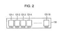
- the main storage memory 13 includes a plurality of DIMM's 130.
- Each DIMM 130 includes 18 memory chips 131-1 to 131-8 as illustrated in Fig. 2 .
- Each memory chip 131-1 to 131-18 has a data with of 4 bits.
- Fig. 2 is a diagram illustrating the structure of the DIMM 130, and an address line or the like except data lines is omitted.
- the main storage memory 13 using the DIMM's 130 capable of correcting data by using an ECC has a data width of, for example, 8 bytes+1 byte (72 bits).
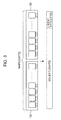
- S 4 EC-D 4 ED may be provided by providing a check bit of 16 bits with respect to data of 16 bytes. Since the ratio of the data and the check bit in this case is 8:1, as illustrated in Fig. 3 , there is no bit for storing extra data in the DIMM 130.
- Fig. 3 is a diagram illustrating the case where a detection and correction processing of the data width of 16 bytes is provided by using two DIMM's 130.
- Fig. 4 is a diagram illustrating the case where an error detection and correction processing in which two reading by 2 interleave is regarded as one unit is executed by using two DIMM's 130.
- an encoding circuit and a decoding circuit capable of high speed processing using (36, 33) Reed-Solomon code in a Galois extension field GF (2 8 ) as an S 8 EC-D 8 ED code are constituted.
- P(x) X 8 +X 4 +X 3 +X 2 +1 is used for 8th order primitive polynomial P(x) in the Galois field GF(2).
- S 8 EC-D 8 ED is a code capable of correcting 1 byte error and detecting 2 byte error.
- Generator polynomial G(X) of the (36, 33) Reed-Solomon code may be expressed by the following expression.
- G x x + ⁇ 0 ⁇ x + ⁇ 1 ⁇ x + ⁇ 2
- the problem when the encoding processing is provided by a high-speed hardware circuit is a portion of the aforementioned polynomial remainder calculation. If the polynomial remainder calculation may be expressed by the form of a generator matrix similar to the existing SEC-DED ECC, it becomes easy to mount the encoding processing on hardware.
- i indicate the byte position (byte 0 to 32) of a block of 33 bytes
- j indicates the bit position (bit 0 to 7) in the byte block
- each d is 0 or 1.
- D i ⁇ bit string in which only (263-i)-th is 1 and the others are 0 ⁇
- I i (x) is a polynomial corresponding to each data bit string D i
- the polynomial C i (x) of the error correction code is expressed as below.
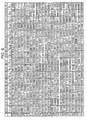
- FIG. 5 and Fig. 6 are diagrams illustrating an example of the generator matrix obtained as described above.
- generator matrix c 23 to c 0 are illustrated for block numbers Block 35 to Block 3 partitioned for every byte.
- the block numbers Block 2 to Block 0 are assigned for error correction code of 24 bits.
- a protection action may be made. For example, some of C n is inverted and stored in the DIMM 130. Note that such a protection action itself is well known, so that the description will be omitted.
- Fig. 7 is a block diagram illustrating the encoding circuit
- Fig. 8 is a circuit diagram illustrating the structure of an EOR circuit tree of the encoding circuit.
- the encoding circuit is provided inside the processor 11 or outside the processor 11 in the node 1.
- the EOR circuit tree 21 includes EOR circuits 211 connected as illustrated in Fig. 8 , and output CheckBit[23] with respect to Data[262] to Data[5].
- the EOR circuit tree 21 obtains EOR for every bit of "1" in the generator matrix illustrated in Figs. 6 and 7 .
- Data and the CheckBit of an error correction code are stored in the main storage memory 13 (DIMM 130) as illustrated with Fig. 4 .
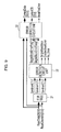
- Fig. 9 is a block diagram illustrating a decoding circuit.
- the decoding circuit includes an EOR circuit tree 31, an error detection circuit unit 32, and an error correction circuit unit 33 which are connected as illustrated in Fig. 9 .
- the decoding circuit is provided inside the processor 11 or outside the processor 11 in the node 1.
- the EOR circuit tree 31 has the same structure as the EOR tree 21 illustrated in Fig. 8 , so that the diagram and description are omitted.
- the EOR circuit tree 31 generates syndrome0[7:0], syndrome1[7:0], syndrome2[7:0] described below based on the encoded data ReadData[263:0] and check bit ReadCheckBit[23:0].
- the syndromes are expressed by S 0 , S 1 , S 2 .
- the code read from the main storage memory 13 DIMM 130
- Y(x) 36 bytes for both of the data and check bit
- Y(x) is a polynomial representation of the code which is a target for which an error is detected (that is, error detection target).
- the syndromes S 0 , S 1 , S 2 is also expressed by linear combination in which only one is 1 in a bit string formed by read data and check bit.
- the method for obtaining the matrix for obtaining the syndromes S 0 , S 1 , S 2 is similar to the method used when encoding, so that the description will be omitted.
- S 0 ⁇ S0 i ⁇ i
- S 1 ⁇ S1 i ⁇ i
- S 2 ⁇ S2 i ⁇ i
- each S 0 S 1 S 2 is the value 0 or 1.
- Fig. 10 and Fig. 11 are diagrams illustrating an example of a matrix for obtaining the syndromes.
- Fig. 10 and Fig. 11 illustrate generator matrix elements S0 7 to S0 0 of the syndrome S 0 , generator matrix elements S1 7 to S1 0 of the syndrome S 1 , generator matrix elements S2 7 to S2 0 of the syndrome S 2 for the block number Block35 to Block0.
- Fig. 12 is a circuit diagram illustrating the error detection circuit unit 32.
- the error detection circuit unit 32 includes a decode/encode circuit 41, an adder circuit 42 with an index number part mod255, an error judging circuit 43, an inverter circuit 44, and a rearrangement circuit 45.
- Fig. 13 is a diagram illustrating an example of the logarithmic conversion, and illustrates a content of a logarithmic conversion chart.
- three decode/encode circuits 41 outputs syndrome Alog-Syndrome0[7:0], Alog_Syndrome1[7:0], Alog_Syndrome2[7:0] after logarithmic conversion, and outputs SingleBlockErrorData[7:0] indicating one block error.
- the adder circuit 42 includes an accumulator 421, an AND circuit 422, an OR circuit 423, and an increment circuit 424. A carry bit of the accumulator 421 is input in the OR circuit 423. The carry bit of the increment circuit 424 is ignored.
- the adder circuit 42 executes remainder calculation including mod255 operation in order to calculate judgment of a block error and the position of the block error.
- the syndrome Alog_Syndrome0[7:0] output from the decode/encode circuit 41 at the most upper side is input in the adder circuit 42 at the upper side via the inverter circuit 44
- the syndrome Alog_Syndrome1[7:0] output from the second decode/encode circuit 41 from the top is input in the adder circuit 42 at the upper side.
- the adder circuit 42 at the upper side outputs SingleBlockErrorPos[7:0] indicating the position (that is, the position of the byte which is to be corrected) p of one block error.
- the syndrome Alog_Syndrome0[7:0] output from the decode/encode circuit 41 at the most upper side is input in the adder circuit 42 at the lower side
- the syndrome Alog_Syndrome2[7:0] output from the decode/encode circuit 41 at the most lower side is input in the adder circuit 42 at the lower side.
- the error judging circuit 43 includes an accumulator 431, a matching detection circuit 432, an inverter circuit 433, an AND circuit 434, and a NOR circuit 435.
- Syndrome0[7:0], Syndrome1[7:0], Syndrome2[7:0] output from the EOR tree 31 are input in the accumulator 431.
- Bit No_Error indicating that there is no error is output from the accumulator 431.
- Alog_Syndrome1[6:7,0] output from a rearrangement circuit 45 that executes rearrangement of bit of the syndrome Alog_Syndrome1[7:0] output from the second decode/encode circuit 41 from the top, and Alog_Syn2_PL_Syn0_mod[7:0] of the adder circuit 42 at the lower side are input in the matching detection circuit 432 as illustrated in Fig. 12 .
- Bit SingleBlockError indicating one block error is output from the AND circuit 434.
- Bit DoubleBlockError indicating two block error is output from the NOR circuit 435.
- Fig. 14 is a circuit diagram illustrating the error correction circuit unit 33.
- the error correction circuit unit 33 includes a decode circuit 51, 36 AND circuits 52, and 36 EOR circuits 53 that are connected as illustrated in Fig. 14 .
- SingleBlockErrorPos[7:0] indicating the position p of one block error output from the adder circuit 42 at the upper side in Fig. 12 is input in the decode circuit 51.
- the output of 36 bits of the decode circuit 51 is input in the corresponding AND circuits 52. Further, the decode circuit 51 outputs value BlockPosError indicating the position of not less than one block error.
- SingleBlockErrorData[7:0] indicating one block error output from the decode/encode circuit 41 is also input in each AND circuit 52.
- Output of the corresponding AND circuit 52 and data ReadData[253:255] to ReadData[7:0] are input in the 33 EOR circuits 53 at the upper side, and the 33 EOR circuits 53 at the upper side outputs correction data CorrectData[263:255] to CorrectData[7:0].
- output of the corresponding AND circuit 52 and check bit ReadCheckBit[23:16], ReadCheckBit[15:8], ReadCheckBit[7:0] are input in the three EOR circuits 53 at the lower side, and the three EOR circuits 53 at the lower side output correction check bit CorrectCB[23:16], CorrectCB[15:8], CorrectCB[7:0]. That is, correction data CorrectData[263:0], correction check bit CorrectCB[23:0], and value BlockPosError indicating the position not less than one block error are output from the error correction circuit unit 33.
- the correction data CorrectData[263:0] output from the error correction circuit unit 33 becomes correct data to which an error correction processing is subjected (that is, after correction)
- the correction data may be used in the case of not a two block error.
- a circuit portion generating the correction check bit CorrectCB[23:0] among the error correction circuit unit 33 may be omitted.
- the value of SignalBlockErrorData[7:0] indicating the position p of one block error is not within the range of 0 to 35, that is, not less than 36, it is judged to be much block error, and is dealt similar to tow block error.
- the circuit scale of the encoding circuit is 24 EOR circuits of about 140 bits.
- the latency of the encoding circuit is about 9 steps of EOR circuits of 2 bits since an EOR circuit tree is used.
- the scale of the circuit for generating syndromes is 24 EOR circuits of about 140 bits.
- the latency of the circuit for generating syndromes is about 9 steps of EOR circuits of 2 bits since an EOR circuit tree is used similarly to the encoding circuit.
- the error detection circuit unit and the error correction circuit unit require at leas three circuits for logarithmic conversion from 8 bits to 8 bits in order to execute an error correction processing from a generated syndrome, one 8 bit accumulator and matching detection circuit for error judgment, and one circuit for correcting a single block (AND-EOR circuit corresponding to 264 bits).
- the 8 bit decode/encode circuit that functions as a logarithmic conversion circuit is constituted by an AND-OR circuit. Accordingly, it is important that the latency of the error detection circuit unit and error correction circuit unit is slightly longer than that of the circuit that generates a syndrome.
- the check bit of ECC that is simplified as in the aforementioned embodiment makes it possible to correct data even when one chip among the DIMM 130 is broken down.
- 33 bytes among 36 bytes becomes a data area (32 bytes is original data, one byte is a space area that is newly ensured for extra data) as illustrated in Fig. 4 .
- the main storage memory 13 stores check bit at, for example, the portion of 1 (2 bytes) of the ratio of 8:1.
- the same reliability of data as in the past is assured even when check bit is stored in the portion of 1 (3 bytes) of the ratio of 11:1 as illustrated in Fig. 4 .
- a space area capable of storing extra data (or information) of one byte may be ensured in the main storage memory 13 by reducing the number of check bit to be required while maintaining the same error correction and detection performance as in the past with respect to 32 byte data.
- directory information of ccNUMA, key information of the main frame, and the like may be stored. That is, a part of the area of the main storage memory 13 may be used for string information for keeping cache coherency, information for assuring data, information for protecting a memory, and the like while keeping the same error correction and detection performance as in the past.
Landscapes
- Physics & Mathematics (AREA)
- Engineering & Computer Science (AREA)
- Theoretical Computer Science (AREA)
- General Physics & Mathematics (AREA)
- Mathematical Physics (AREA)
- General Engineering & Computer Science (AREA)
- Pure & Applied Mathematics (AREA)
- Algebra (AREA)
- Probability & Statistics with Applications (AREA)
- Quality & Reliability (AREA)
- Computational Mathematics (AREA)
- Mathematical Analysis (AREA)
- Mathematical Optimization (AREA)
- Computing Systems (AREA)
- Error Detection And Correction (AREA)
- Techniques For Improving Reliability Of Storages (AREA)
- Detection And Correction Of Errors (AREA)
Applications Claiming Priority (1)
| Application Number | Priority Date | Filing Date | Title |
|---|---|---|---|
| JP2008294828A JP5422974B2 (ja) | 2008-11-18 | 2008-11-18 | 誤り判定回路及び共有メモリシステム |
Publications (2)
| Publication Number | Publication Date |
|---|---|
| EP2187527A2 true EP2187527A2 (fr) | 2010-05-19 |
| EP2187527A3 EP2187527A3 (fr) | 2012-10-10 |
Family
ID=42045253
Family Applications (1)
| Application Number | Title | Priority Date | Filing Date |
|---|---|---|---|
| EP09174357A Ceased EP2187527A3 (fr) | 2008-11-18 | 2009-10-28 | Circuit de jugement d'erreur et système de mémoire partagée |
Country Status (5)
| Country | Link |
|---|---|
| US (1) | US8327236B2 (fr) |
| EP (1) | EP2187527A3 (fr) |
| JP (1) | JP5422974B2 (fr) |
| KR (1) | KR101050744B1 (fr) |
| CN (1) | CN101740135A (fr) |
Cited By (2)
| Publication number | Priority date | Publication date | Assignee | Title |
|---|---|---|---|---|
| EP2645249A1 (fr) * | 2012-03-30 | 2013-10-02 | Fujitsu Limited | Appareil de traitement dýinformations et procédé de contrôle d'appareil de traitement dýinformations |
| CN105808497A (zh) * | 2014-12-30 | 2016-07-27 | 华为技术有限公司 | 一种数据处理方法 |
Families Citing this family (8)
| Publication number | Priority date | Publication date | Assignee | Title |
|---|---|---|---|---|
| US7539924B1 (en) | 2005-11-15 | 2009-05-26 | Western Digital Technologies, Inc. | Disk drive implementing data path protection by encoding large host blocks into sub blocks |
| US8397107B1 (en) * | 2009-12-11 | 2013-03-12 | Western Digital Technologies, Inc. | Data storage device employing data path protection using both LBA and PBA |
| JP2012177964A (ja) * | 2011-02-25 | 2012-09-13 | Nec Computertechno Ltd | メモリシステム及びメモリモジュール制御方法 |
| JP5601256B2 (ja) * | 2011-03-20 | 2014-10-08 | 富士通株式会社 | メモリコントローラ及び情報処理装置 |
| US8671250B2 (en) | 2011-12-15 | 2014-03-11 | Western Digital Technologies, Inc. | Data storage device generating redundancy for data path protection of a parity sector |
| US9362953B2 (en) * | 2013-08-02 | 2016-06-07 | Infineon Technologies Ag | Efficient error correction of multi-bit errors |
| US11061772B2 (en) | 2018-12-14 | 2021-07-13 | Samsung Electronics Co., Ltd. | FPGA acceleration system for MSR codes |
| KR20210138241A (ko) | 2020-05-12 | 2021-11-19 | 삼성전자주식회사 | 메모리 컨트롤러, 메모리 시스템 및 메모리 모듈 |
Citations (5)
| Publication number | Priority date | Publication date | Assignee | Title |
|---|---|---|---|---|
| JPS5457848A (en) | 1977-10-15 | 1979-05-10 | Nippon Telegr & Teleph Corp <Ntt> | Detecting correction system for block error |
| US4637021A (en) | 1983-09-28 | 1987-01-13 | Pioneer Electronic Corporation | Multiple pass error correction |
| US5226043A (en) | 1990-12-27 | 1993-07-06 | Raytheon Company | Apparatus and method for data error detection and correction and address error detection in a memory system |
| US20040236901A1 (en) | 2003-05-10 | 2004-11-25 | Briggs Theodore C. | Systems and methods for buffering data between a coherency cache controller and memory |
| JP2006252545A (ja) | 2005-03-09 | 2006-09-21 | Hewlett-Packard Development Co Lp | 外部raid対応キャッシュ |
Family Cites Families (27)
| Publication number | Priority date | Publication date | Assignee | Title |
|---|---|---|---|---|
| US4162480A (en) * | 1977-01-28 | 1979-07-24 | Cyclotomics, Inc. | Galois field computer |
| EP0096165B1 (fr) * | 1982-06-15 | 1988-06-08 | Kabushiki Kaisha Toshiba | Appareil pour diviser les éléments d'un champ de Galois |
| JPS58219852A (ja) * | 1982-06-15 | 1983-12-21 | Toshiba Corp | エラ−訂正回路 |
| JPS61126826A (ja) * | 1984-11-22 | 1986-06-14 | Hiroichi Okano | 倍長単一誤り訂正2重誤り検出リ−ド・ソロモン符号の復号器 |
| JPH01158828A (ja) * | 1987-12-15 | 1989-06-21 | Victor Co Of Japan Ltd | 誤り検出・訂正装置 |
| JP2810397B2 (ja) | 1989-02-16 | 1998-10-15 | キヤノン株式会社 | 誤り訂正装置 |
| CA2019351A1 (fr) * | 1989-07-06 | 1991-01-06 | Francis H. Reiff | Memoire insensible aux defaillances |
| US5325370A (en) * | 1991-11-12 | 1994-06-28 | Storage Technology Corporation | Method and apparatus for recording data on magnetic tape media |
| KR100253171B1 (ko) | 1992-06-02 | 2000-04-15 | 구자홍 | 데이타 오류정정 방법 및 회로 |
| JPH07226687A (ja) * | 1994-02-10 | 1995-08-22 | Matsushita Electric Ind Co Ltd | 誤り訂正処理装置 |
| SG24105A1 (en) * | 1994-03-19 | 1996-02-10 | Sony Corp | Apparatus for recording and reproducing information |
| IN188196B (fr) * | 1995-05-15 | 2002-08-31 | Silicon Graphics Inc | |
| JPH10255402A (ja) * | 1997-03-10 | 1998-09-25 | Fujitsu Ltd | 磁気ディスク装置 |
| JPH1117557A (ja) | 1997-05-01 | 1999-01-22 | Mitsubishi Electric Corp | 誤り訂正方法及び誤り訂正装置 |
| DE19982502T1 (de) * | 1998-01-08 | 2000-11-30 | Seagate Technology | Vorrichtung, System und Verfahren einer physischen Blockadressen-Wiederherstellung für zyklische Fehlerkorrektur-Codes |
| JP3678574B2 (ja) | 1998-02-09 | 2005-08-03 | 日本電気エンジニアリング株式会社 | チェックビット生成回路及びエラー訂正回路並びにそれ等を使用したecc制御回路 |
| JP4105819B2 (ja) * | 1999-04-26 | 2008-06-25 | 株式会社ルネサステクノロジ | 記憶装置およびメモリカード |
| JP3345385B2 (ja) * | 2000-01-18 | 2002-11-18 | 松下電器産業株式会社 | チェンサーチ装置 |
| JP3668673B2 (ja) * | 2000-06-09 | 2005-07-06 | 株式会社日立コミュニケーションテクノロジー | エラー訂正符号の構成方法、復号方法、伝送装置、ネットワーク |
| GB2380598B (en) * | 2000-10-04 | 2003-09-03 | Global Silicon Ltd | Deinterleaving data |
| TW522657B (en) * | 2002-01-17 | 2003-03-01 | Via Tech Inc | PGZ algorithm based multi-mode Reed-Solomon decoder and its method |
| US7437651B2 (en) * | 2004-06-29 | 2008-10-14 | Hewlett-Packard Development Company, L.P. | System and method for controlling application of an error correction code (ECC) algorithm in a memory subsystem |
| GB2428496A (en) | 2005-07-15 | 2007-01-31 | Global Silicon Ltd | Error correction for flash memory |
| US7600176B2 (en) * | 2006-03-07 | 2009-10-06 | Broadcom Corporation | Performing multiple Reed-Solomon (RS) software error correction coding (ECC) Galois field computations simultaneously |
| US7721140B2 (en) * | 2007-01-02 | 2010-05-18 | International Business Machines Corporation | Systems and methods for improving serviceability of a memory system |
| JP2008242034A (ja) * | 2007-03-27 | 2008-10-09 | Japan Aerospace Exploration Agency | データ圧縮/伸張と暗号化/復号と誤り制御とを行う統合符号化及び復号装置、並びに方法 |
| TWI334277B (en) * | 2007-06-06 | 2010-12-01 | Lite On Technology Corp | Method for calculating syndrome efficiently in reed-solomon decoding and machine readable storage medium storing instructions for performing the method |
-
2008
- 2008-11-18 JP JP2008294828A patent/JP5422974B2/ja not_active Expired - Fee Related
-
2009
- 2009-10-23 US US12/604,544 patent/US8327236B2/en not_active Expired - Fee Related
- 2009-10-28 EP EP09174357A patent/EP2187527A3/fr not_active Ceased
- 2009-11-16 CN CN200910212292A patent/CN101740135A/zh active Pending
- 2009-11-17 KR KR1020090110818A patent/KR101050744B1/ko not_active IP Right Cessation
Patent Citations (5)
| Publication number | Priority date | Publication date | Assignee | Title |
|---|---|---|---|---|
| JPS5457848A (en) | 1977-10-15 | 1979-05-10 | Nippon Telegr & Teleph Corp <Ntt> | Detecting correction system for block error |
| US4637021A (en) | 1983-09-28 | 1987-01-13 | Pioneer Electronic Corporation | Multiple pass error correction |
| US5226043A (en) | 1990-12-27 | 1993-07-06 | Raytheon Company | Apparatus and method for data error detection and correction and address error detection in a memory system |
| US20040236901A1 (en) | 2003-05-10 | 2004-11-25 | Briggs Theodore C. | Systems and methods for buffering data between a coherency cache controller and memory |
| JP2006252545A (ja) | 2005-03-09 | 2006-09-21 | Hewlett-Packard Development Co Lp | 外部raid対応キャッシュ |
Non-Patent Citations (1)
| Title |
|---|
| AKASH KUMAR ET AL: "Vectorization of Reed Solomon Decoding and Mapping on the EVP", 2008 DESIGN, AUTOMATION AND TEST IN EUROPE : MUNICH, GERMANY, 10 - 14 MARCH 2008, PISCATAWAY, NJ : IEEE SERVICE CENTER, US, 10 March 2008 (2008-03-10), pages 450 - 455, XP031241837, ISBN: 978-3-9810801-3-1 * |
Cited By (5)
| Publication number | Priority date | Publication date | Assignee | Title |
|---|---|---|---|---|
| EP2645249A1 (fr) * | 2012-03-30 | 2013-10-02 | Fujitsu Limited | Appareil de traitement dýinformations et procédé de contrôle d'appareil de traitement dýinformations |
| CN103365792A (zh) * | 2012-03-30 | 2013-10-23 | 富士通株式会社 | 信息处理设备和控制信息处理设备的方法 |
| US8910004B2 (en) | 2012-03-30 | 2014-12-09 | Fujitsu Limited | Information processing apparatus, and method of controlling information processing apparatus |
| CN105808497A (zh) * | 2014-12-30 | 2016-07-27 | 华为技术有限公司 | 一种数据处理方法 |
| CN105808497B (zh) * | 2014-12-30 | 2018-09-21 | 华为技术有限公司 | 一种数据处理方法 |
Also Published As
| Publication number | Publication date |
|---|---|
| JP2010122828A (ja) | 2010-06-03 |
| KR20100056389A (ko) | 2010-05-27 |
| CN101740135A (zh) | 2010-06-16 |
| JP5422974B2 (ja) | 2014-02-19 |
| EP2187527A3 (fr) | 2012-10-10 |
| US8327236B2 (en) | 2012-12-04 |
| US20100125771A1 (en) | 2010-05-20 |
| KR101050744B1 (ko) | 2011-07-21 |
Similar Documents
| Publication | Publication Date | Title |
|---|---|---|
| US8327236B2 (en) | Error judging circuit and shared memory system | |
| US5418796A (en) | Synergistic multiple bit error correction for memory of array chips | |
| US8762821B2 (en) | Method of correcting adjacent errors by using BCH-based error correction coding | |
| US5099484A (en) | Multiple bit error detection and correction system employing a modified Reed-Solomon code incorporating address parity and catastrophic failure detection | |
| EP0535086B1 (fr) | Correction d'erreurs multiples dans une memoire d'ordinateur | |
| US6662333B1 (en) | Shared error correction for memory design | |
| US20040260994A1 (en) | Method for constructing erasure correcting codes whose implementation requires only exclusive ORs | |
| JPH02278921A (ja) | 2進データの符号化及び復号のための方法及び復号装置 | |
| US4631725A (en) | Error correcting and detecting system | |
| US20050188292A1 (en) | Method and apparatus for encoding special uncorrectable errors in an error correction code | |
| Pontarelli et al. | Low delay single symbol error correction codes based on reed solomon codes | |
| US8566679B2 (en) | Error-correcting encoding method with total parity bits, and method for detecting multiple errors | |
| CN113297001B (zh) | 一种raid编解码方法及编解码电路 | |
| US20050149834A1 (en) | (18, 9) Error correction code for double error correction and triple error detection | |
| JP4790790B2 (ja) | 誤り検出訂正回路及び半導体メモリ | |
| US20190273515A1 (en) | Apparatuses and methods for interleaved bch codes | |
| Silva et al. | An extensible code for correcting multiple cell upset in memory arrays | |
| US20060294447A1 (en) | Apparatus and method for parity generation in a data-packing device | |
| US8739006B2 (en) | Reduced circuit implementation of encoder and syndrome generator | |
| WO2008051385A2 (fr) | Allocation de données sur des puces de mémoire | |
| US6460157B1 (en) | Method system and program products for error correction code conversion | |
| US4868829A (en) | Apparatus useful for correction of single bit errors in the transmission of data | |
| CN106021012B (zh) | 数据处理电路 | |
| US11694761B2 (en) | Method to increase the usable word width of a memory providing an error correction scheme | |
| JP2006323434A (ja) | データ処理装置及びそのメモリ訂正方法 |
Legal Events
| Date | Code | Title | Description |
|---|---|---|---|
| PUAI | Public reference made under article 153(3) epc to a published international application that has entered the european phase |
Free format text: ORIGINAL CODE: 0009012 |
|
| AK | Designated contracting states |
Kind code of ref document: A2 Designated state(s): AT BE BG CH CY CZ DE DK EE ES FI FR GB GR HR HU IE IS IT LI LT LU LV MC MK MT NL NO PL PT RO SE SI SK SM TR |
|
| AX | Request for extension of the european patent |
Extension state: AL BA RS |
|
| PUAL | Search report despatched |
Free format text: ORIGINAL CODE: 0009013 |
|
| AK | Designated contracting states |
Kind code of ref document: A3 Designated state(s): AT BE BG CH CY CZ DE DK EE ES FI FR GB GR HR HU IE IS IT LI LT LU LV MC MK MT NL NO PL PT RO SE SI SK SM TR |
|
| AX | Request for extension of the european patent |
Extension state: AL BA RS |
|
| RIC1 | Information provided on ipc code assigned before grant |
Ipc: H03M 13/15 20060101AFI20120904BHEP Ipc: G06F 11/10 20060101ALI20120904BHEP |
|
| 17P | Request for examination filed |
Effective date: 20130218 |
|
| 17Q | First examination report despatched |
Effective date: 20130419 |
|
| STAA | Information on the status of an ep patent application or granted ep patent |
Free format text: STATUS: THE APPLICATION HAS BEEN REFUSED |
|
| 18R | Application refused |
Effective date: 20150119 |