EP2175371A1 - Appareils de contrôle de synchronisation, appareils de traitement d'informations, et procédés de gestion de synchronisation - Google Patents
Appareils de contrôle de synchronisation, appareils de traitement d'informations, et procédés de gestion de synchronisation Download PDFInfo
- Publication number
- EP2175371A1 EP2175371A1 EP09170690A EP09170690A EP2175371A1 EP 2175371 A1 EP2175371 A1 EP 2175371A1 EP 09170690 A EP09170690 A EP 09170690A EP 09170690 A EP09170690 A EP 09170690A EP 2175371 A1 EP2175371 A1 EP 2175371A1
- Authority
- EP
- European Patent Office
- Prior art keywords
- processor
- synchronization
- cpu
- resynchronization
- timeout time
- Prior art date
- Legal status (The legal status is an assumption and is not a legal conclusion. Google has not performed a legal analysis and makes no representation as to the accuracy of the status listed.)
- Granted
Links
Images


Classifications
-
- G—PHYSICS
- G06—COMPUTING; CALCULATING OR COUNTING
- G06F—ELECTRIC DIGITAL DATA PROCESSING
- G06F11/00—Error detection; Error correction; Monitoring
- G06F11/07—Responding to the occurrence of a fault, e.g. fault tolerance
- G06F11/16—Error detection or correction of the data by redundancy in hardware
- G06F11/1629—Error detection by comparing the output of redundant processing systems
- G06F11/165—Error detection by comparing the output of redundant processing systems with continued operation after detection of the error
-
- G—PHYSICS
- G06—COMPUTING; CALCULATING OR COUNTING
- G06F—ELECTRIC DIGITAL DATA PROCESSING
- G06F13/00—Interconnection of, or transfer of information or other signals between, memories, input/output devices or central processing units
- G06F13/14—Handling requests for interconnection or transfer
- G06F13/20—Handling requests for interconnection or transfer for access to input/output bus
- G06F13/24—Handling requests for interconnection or transfer for access to input/output bus using interrupt
-
- G—PHYSICS
- G06—COMPUTING; CALCULATING OR COUNTING
- G06F—ELECTRIC DIGITAL DATA PROCESSING
- G06F11/00—Error detection; Error correction; Monitoring
- G06F11/07—Responding to the occurrence of a fault, e.g. fault tolerance
- G06F11/16—Error detection or correction of the data by redundancy in hardware
- G06F11/1629—Error detection by comparing the output of redundant processing systems
- G06F11/1641—Error detection by comparing the output of redundant processing systems where the comparison is not performed by the redundant processing components
-
- G—PHYSICS
- G06—COMPUTING; CALCULATING OR COUNTING
- G06F—ELECTRIC DIGITAL DATA PROCESSING
- G06F11/00—Error detection; Error correction; Monitoring
- G06F11/07—Responding to the occurrence of a fault, e.g. fault tolerance
- G06F11/16—Error detection or correction of the data by redundancy in hardware
- G06F11/1675—Temporal synchronisation or re-synchronisation of redundant processing components
- G06F11/1679—Temporal synchronisation or re-synchronisation of redundant processing components at clock signal level
-
- G—PHYSICS
- G06—COMPUTING; CALCULATING OR COUNTING
- G06F—ELECTRIC DIGITAL DATA PROCESSING
- G06F13/00—Interconnection of, or transfer of information or other signals between, memories, input/output devices or central processing units
- G06F13/38—Information transfer, e.g. on bus
-
- G—PHYSICS
- G06—COMPUTING; CALCULATING OR COUNTING
- G06F—ELECTRIC DIGITAL DATA PROCESSING
- G06F13/00—Interconnection of, or transfer of information or other signals between, memories, input/output devices or central processing units
- G06F13/38—Information transfer, e.g. on bus
- G06F13/42—Bus transfer protocol, e.g. handshake; Synchronisation
Definitions
- the present invention relates to a synchronization control apparatus, an information processing apparatus, and a synchronization management method.
- a synchronization control apparatus which monitors an existence or otherwise of a synchronization delay between the two CPU's, and executes and retries a resynchronization process which, in the event that a synchronization delay has occurred, resynchronizes a CPU in which a failure has occurred by resetting and initializing it.
- Patent Document 1 Japanese Laid-open Patent Application No. 2006-302289
- Patent Document 2 Japanese Laid-open Patent Application No. 2005-285119
- a synchronization control apparatus includes a counter that carries out a counting and outputs resulting count information, a timeout time holder that holds a predetermined timeout time and outputs the timeout time, a comparator that compares the count information output from the counter and the timeout time output from the timeout time holder, a synchronization controller that monitors a synchronization between a first processor and a second processor by comparing an output from the first processor and an output from the second processor and starts a counting, when a mis-match of the outputs from the first processor and the second processor is detected and wherein the comparator detects that the count information and the timeout time match, the comparator stops either the first processor or second processor in which a synchronization delay has occurred.
- FIG. 1 is a block diagram depicting an example configuration of the server system.
- the server system is realized as a multiprocessor system including a plurality of system boards (#0 to #n) 1.
- the plurality of system boards (#0 to #n) 1 are mutually connected through a global address crossbar 3 and global data crossbar 4.
- the global address crossbar 3 and global data crossbar 4 are also connected to a plurality of IO units (#0 to #n) 2 corresponding to the system boards (#0 to #n) 1 with the same plurality of serial numbers (#0 to #n).
- the global address crossbar 3 is an address relay unit which relays a command issued from each system board (#0 to #n) 1, and an address which is an object of the command, to another system board (#0 to #n) 1 and IO unit (#o to #n) 2.
- the global data crossbar 4 is a processing unit which relays data between the system boards (#0 to #n) 1, between the IO units (#0 to #n) 2, and between the system boards (#0 to #n) 1 and IO units (#0 to #n) 2.
- a system control/management apparatus 5 is connected to the system boards (#0 to #n) 1 and IO units (#0 to #n) 2.
- the system control/management apparatus 5 is a service processor or console apparatus which, in accordance with a control signal input by a system manager, carries out an overall management, such as a setting of various kinds of setting value in a register group (the details of which will be described hereafter based on FIGS. 2 and 3 ) included in each system board (#0 to #n) 1 and IO unit (#0 to #n) 2, and a setting of a configuration of a partition.
- the partition is a system configured by a combination of the system boards (#0 to #n) 1 and IO units (#0 to #n) 2.
- FIG. 2 is a block diagram depicting a circuit configuration mounted on each system board (#0 to #n) 1.
- a CPU0 6 acting as a first processor, and a CPU1 6 acting as a second processor are installed on the system board 1 in a condition in which they are connected to corresponding CPU bus0 7 and CPU bus1 7.
- the CPU0 6 and the CPU1 6 are a pair of CPU's made redundant (redundant CPU's) which, as well as having the same configuration, are operated in synchronization.
- the information processing apparatus configured of the multiprocessor (redundant CPU) system mounted on the system board 1 is comprised of the plurality of CPUs of CPU0 6 and CPU1 6 and a plurality of buses of CPU bus0 7 and CPU bus1 7, clock control circuits 23 and 23, a firmware hub 15, a north bridge 6, a memory 12, and a memory controller 10.
- the command and address notified of from the global address crossbar 3 are input into each CPU0 6 and CPU1 6 through each CPU bus0 7 and CPU bus1 7, as well as being input into the firmware hub 15 and memory controller 10.
- the clock control circuits 23 and 23to pass through, or block them, are controlled by a switching/resynchronization control circuit 14, to be described hereafter, in the north bridge 6.
- the clock control circuits 23 and 23 are switches which allow clocks (external clocks acting as first clocks), supplied to the CPU bus0 7 and the CPU bus1 7 from a not depicted clock generation device provided outside the system board 1, to pass through, or block them.
- the CPU0 6 and the CPU1 6 which, being connected to the CPU bus0 7 and CPU bus1 7, are prevented by the clock control circuits 23 from being supplied with the clocks, become inoperative, and degenerate because the clocks are not input thereinto.
- the firmware hub 15 is connected to each CPU0 6 and CPU1 6 for such a reading.
- the firmware hub 15 is a nonvolatile flash memory storing firmware (e.g. BIOS (Basic Input Output System)) which is read first when each CPU0 6 and CPU1 6 is subjected to a CPU reset or interrupt, as heretofore described.
- BIOS Basic Input Output System
- Each CPU0 6 and CPU1 6 also executes an initial process (the "reset firmware initial process” depicted in FIGS. 4A and 4B ) in the event that it is subjected to the reset.
- the memory controller 10 executes a write process which writes data input from the global data crossbar 4 into a storage position of the memory 12 indicated by the input address.
- the memory controller 10 is connected to the memory 12 in which various kinds of data are stored.
- the memory controller 10 also executes a read process which reads data retrieved from the storage position, and sends them to the global data crossbar 4 or each CPU0 6 and CPU1 6.
- the north bridge 6 detects that a failure and degeneration has occurred, causing a synchronization break, in one CPU (one module CPU) of the CPU0 6 and the CPU1 6 configuring the redundant CPU's.
- the north bridge 6 is a circuit group which corresponds to a synchronization control apparatus.
- the north bridge 6 carries out a redundant CPU resynchronization process in synchronization with a CPU0 6 or a CPU1 6 operating in accordance with the firmware stored in the firmware hub 15.
- the "synchronization break” referring to the fact that the pair of CPU's configuring the redundant CPU's cannot be operated in synchronization, originates with a "synchronization delay".
- the process executed by one CPUO 6 or CPU1 6 lags behind the process executed by the other CPU0 6 or CPU1 6.
- the "redundant CPU resynchronization process” is a process for returning both the CPU0 6 and the CPU1 6 to a redundant configuration again.
- the north bridge 6 is configured of hardware which operates independently of the CPU0 6 and the CPU1 6, it is possible to execute such a redundant CPU resynchronization process without causing a shutdown/restart of an OS operating on the system.
- inspection circuits 11 and 11 configure the north bridge 6.
- a CPU bus synchronization inspection circuit 13 configures the switching/resynchronization control circuit 14, a resynchronization timer and timeout control circuit 16, a changeover switch 17, a reset control register 18, a resynchronization control register 19, an error indication register 20, a command decoder 21, and a phase synchronization circuit (PLL0) 22, which are surrounded by the broken line, configure the north bridge 6.
- PLL0 phase synchronization circuit
- the command decoder 21 decodes a command issued from the system control/management apparatus 5 to the north bridge 6.
- the command decoder 21 then carries out a writing/reading of setting values with respect to the resynchronization control register 19 and the resynchronization timer and timeout control circuit 16 (a resynchronization maximum time setting register 163) in accordance with a result of the decoding.
- the inspection circuits 11 and 11 being connected to the output terminals of the CPU0 6 and the CPU1 6 through the corresponding CPU bus0 7 and CPU bus1 7, receive packets transmitted from the CPU0 6 and the CPU1 6 toward the global address crossbar 3, and carry out an inspection of an ECC (Error Checking and Correcting), a parity, and the like.
- the inspection circuits 11 and 11 give an error notification to the switching/resynchronization control circuit 14 upon detecting an error by means of the inspection.
- the CPU bus synchronization inspection circuit 13 being connected to the CPU bus0 7 and the CPU bus1 7, carries out a synchronization inspection for each CPU bus. That is, the CPU bus synchronization inspection circuit 13 inspects for whether or not the CPU pair configuring the redundant CPU's are carrying out a synchronized operation. Then, the CPU bus synchronization inspection circuit 13 gives an error notification to the switching/resynchronization control circuit 14 upon detecting a desynchronization.
- the CPU0 6 or the CPU1 6 in which the error has been detected gives an error notification (an internal error notification) to the switching/resynchronization control circuit 14.
- the resynchronization timer and timeout control circuit 16 (a timer/maximum time comparison circuit 161), reset control register 18, resynchronization control register 19, changeover switch 17, and error indication register 20 are connected to the switching/resynchronization control circuit 14.
- the changeover switch 17 carries out a switching between the CPU bus0 7 and the CPU bus1 7 in accordance with an instruction from the switching/resynchronization control circuit 14.
- the changeover switch 17 carrying out the switching between the CPU bus0 7 and the sCPU bus1 7, it is decided, for example, through which of the CPU bus0 7 and CPU bus1 7 the issued command is to be input into the global address crossbar 3.
- the reset control register 18 is a register which manages the condition of each CPU0 6 and CPU1 6 for a reset control over each CPU0 6 and CPU1 6. For example, on a saving of cache data of a normal CPU0 6 or a normal CPU1 6 to the memory 12 being completed in the redundant CPU resynchronization process, a saving completion flag corresponding to the normal CPU is put up in the reset control register 18 by the normal CPU's of the CPU0 6 or the CPU1 6 control (the normal CPU interrupt firm process) based on the firmware stored in the firmware hub 15 (S106 and S110).
- the resynchronization control register 19 is a register in which are set the number of resynchronization process executions for the two CPUs of the CPU0 6 and the CPU1 6, an upper limit thereof (a resynchronization possible upper limit), and a resynchronization possibility flag.
- the resynchronization possible upper limit is set by the system control/management device 5 operated by the system manager, via the command decoder 21.
- the resynchronization possibility flag is a flag which indicates whether or not it is possible to resynchronize the two CPUs of the CPU0 6 and the CPU1 6.
- a normal CPU0 6 or a normal CPU1 6 operating in accordance with the firmware stored in the firmware hub 15, as well as recording an actual number of resynchronization process executions in the resynchronization control register 19 (S308), compares it with the resynchronization possible upper limit set in the resynchronization control register 19 (S306 and S307).
- the CPU0 6 or the CPU1 6 determines that it is possible to further retry the resynchronization process, and sets, for example, a flag 1 as the resynchronization possibility flag in the resynchronization control register 19 (S308) but, in the event that the number of executions reaches the resynchronization possible upper limit, it determines that it is impossible to further retry the resynchronization process, and sets, for example, a flag 0 as the resynchronization possibility flag (S309).
- the error indication register 20 is a register which stores information on various kinds of fault detected by the north bridge 6 (the switching/resynchronization control circuit 14, and resynchronization timer and timeout control circuit 16 (timer/maximum timer comparison circuit 161 )). For example, in the event that the switching/resynchronization control circuit 14 has received each heretofore described error notification, error contents notified of are stored in the error indication register 20. Also, an ID of an abnormal CPU bus0 7 or an abnormal CPU bus1 7 in which a synchronization delay has occurred is stored in the error indication register 20.
- a synchronization impossible flag (corresponding to synchronization delay information) is stored in the error indication register 20 acting as a synchronization delay information holder.
- a CPU0 6 or a CPU1 6 which executes the reset firmware initial setting process based on the firmware stored in the firmware hub 15, based on whether or not the synchronization impossible flag is set in the error indication register 20 after a start-up, executes the resynchronization process (in the event that the synchronization impossible flag is not set: in and after S302), or starts independently (in the event that the synchronization impossible flag is set: in and after S310). Then, it is also acceptable to notify the system manager of fault information by, for example, acquiring other error information stored in the error indication register 20, and notifying the system control/management device 5 of the information.
- the resynchronization timer and timeout control circuit 16 is a circuit which compares a resynchronization maximum time set by the system control/management device 5 via the command decoder 21 and time for the resynchronization. In the event that the time exceeds the resynchronization maximum time, the resynchronization timer and timeout control circuit 16 requests the switching/resynchronization control circuit 14 to activate only a normal CPUs of the normal CPU0 6 or the normal CPU1 6 and a normal CPU buses of the normal CPU bus0 7 or the normal CPU bus1 7, and execute a reset.
- the resynchronization timer and timeout control circuit 16 is configured of the resynchronization maximum time setting register 163, a resynchronization timer register 162, and the timer/maximum time comparison circuit 161, as depicted in FIG. 3 .
- a resynchronization process time upper limit (a timeout time) is set in the resynchronization maximum time setting register 163 (corresponding to a timeout time holder) by the system control/management apparatus 5 operated by the system manager, via the command decoder 21.
- the resynchronization timer register 162 (corresponding to a counter) measures a resynchronization time by counting up register values (corresponding to count information) using the clocks (the first clocks) supplied from the phase synchronization circuit (PLL0) 22.
- clocks from the phase synchronization circuit (PLL0) 22 which are of a system differing from that of CPU clocks, it is possible to measure the time without depending upon a condition of each CPU0 6 and CPU1 6, and it does not happen either that the register values are cleared due to a reset for a resynchronization.
- the timer/maximum time comparison circuit 161 (corresponding to a comparator) compares a value of the resynchronization maximum time setting register 163 and a value of the resynchronization timer register 162 and, in the event that the two values match, as well as clearing the resynchronization timer register 162 to zero, and stopping the counting-up (S501), puts up the synchronization impossible flag in the error indication register 20 (S502), and requests the switching/resynchronization control circuit 14 to activate only a normal CPU 6 and normal CPU bus 7, and implement a reset (S503).
- the switching/resynchronization control circuit 14 is a circuit which, by receiving an error notification from each CPU0 6 and CPU1 6, each inspection circuit 11 and 11, or the CPU bus synchronization inspection circuit 13, subjects both, or a normal one, of the two CPUs of the CPU0 6 and the CPU1 6 to a CPU reset or interrupt, controls the operation of the changeover switch 17, and sets a flag in the error indication register 20.
- the switching/resynchronization control circuit 14 in the event of receiving the error notification, by setting the clock control circuit 23 in such a way as to stop a supply of clocks to a CPU bus0 7 or a CPU bus1 7 to which is connected a CPU0 6 or a CPU1 6 in which an error has occurred, deactivates the CPU bus0 7 or the CPU bus1 7 (S002) and, as well as stopping a command issue from the CPU bus0 7 or the CPU bus1 7 to the global address crossbar 3, records which CPU bus0 7 or CPU bus1 7 has deactivated in the error indication register 20.
- the switching/resynchronization control circuit 14 being triggered by receiving the error notification, notifies a normal CPU0 6 or a normal CPU1 6 connected to a normal CPU bus0 7 or a normal CPU bus1 7 of the interrupt (S003).
- the normal CPU0 6 or the normal CPU1 6 executes the "normal CPU interrupt firm process" depicted in FIGS. 4 and 5 , as heretofore described. That is, a processor (a CPU0 6 or a CPU1 6) in which no synchronization delay has occurred is initialized.
- the CPU0 6 or the CPU1 6 to which such a reset has been issued executes the initial process (the "reset firmware initial process" depicted in FIGS. 4A and 4B ), as heretofore described.
- the switching/resynchronization control circuit 14 on being requested by the timer/maximum time comparison circuit 161 to activate only a normal CPU 6 and normal CPU bus 7, and implement a reset, as well as referring to the record of the deactivated CPU bus0 7 or CPU bus1 7 stored in the error indication register 20, and causing an abnormal CPU0 6 or an abnormal CPU1 6 side clock control circuit 23 to stop a supply of clocks to the CPU bus0 7 or the CPU bus1 7 (S503), issues the reset only to the normal CPU0 6 or the normal CPU1 6 (S504), and compels the changeover switch 17 to switch to the normal CPU0 6 or the normal CPU1 6 side (S505).
- the heretofore described CPUs of the CPU0 6 and the CPU1 6, firmware hub 15, CPU bus synchronization inspection circuit 13, and switching/resynchronization control circuit 14 correspond to a synchronization controller which, by comparing an output from the first processor (the CPU0 6) and an output from the second processor (the CPU1 6), monitors a synchronization between the first and second processors (a function of the CPU bus synchronization inspection circuit 13).
- the synchronization controller initializes the counter, and causes the counter to start a counting (functions of the switching/resynchronization control circuit 14, CPU0 6 and CPU1 6, and firmware hub 15).
- the synchronization controller stops either the first or second processor in which a synchronization delay has occurred (a function of the switching/resynchronization control circuit 14).
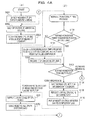
- an ⁇ column indicates the operational sequence of the north bridge 6, and a ⁇ column indicates the flow of the process executed by the CPU0 6 or the CPU1 6 based on the firmware.
- the switching/resynchronization control circuit 14 by powering on a main power supply, starts the operation in ⁇ of FIGS. 4A and 4B and, in a first S001, based on an error notification from each CPU0 6 and CPU1 6, each inspection circuit 11 and 11, or the CPU bus synchronization inspection circuit 13, monitors a synchronization delay of either CPU 6, that is, a redundant CPU synchronization break.
- the switching/resynchronization control circuit 14 on detecting the redundant CPU synchronization break, causes the process to proceed from S001 to S002.
- the switching/resynchronization control circuit 14 stops the ⁇ operation by stopping a supply of clocks to a CPU bus0 7 or a CPU bus1 7 (hereafter referred to as an "abnormal CPU bus 7") to which is connected a CPU0 6 or a CPU1 6 (hereafter referred to as an "abnormal CPU 6) in which a synchronization delay has occurred.
- the switching/resynchronization control circuit 14 gives an interrupt notification that the abnormal CPU 6 is stopped, that is, of a "one module stop", to a CPU0 6 or a CPU 1 6 (hereafter referred to as a "normal CPU 6") connected to a CPU bus0 7 or a CPU bus1 7 (hereafter referred to as a "normal CPU bus 7") on a side whose operation is not stopped.
- the normal CPU 6 which has received the interrupt notification reads the firmware stored in the firmware hub 15, and starts the normal CPU interrupt firm process depicted in ⁇ of FIGS. 4A and 4B . Then, the normal CPU 6, in a first S100 after the start, confirms a condition of the resynchronization timer register 162. Then, in the event that the resynchronization timer register 162 is in the middle of a timer counting, the normal CPU 6 causes the process to proceed directly to S103 and, in the event that the resynchronization timer register 162 has been stopped, and a timer counting has not yet been started, causes the process to proceed to S101.
- the normal CPU 6 records the ID of the CPU bus 7 whose operation has been stopped in S002 in the error indication register 20. On completing S102, the normal CPU 6 causes the process to proceed to S103.
- the normal CPU 6 refers to the resynchronization possibility flag set in the resynchronization control register 19, and determines whether or not it is possible to implement a redundant CPU resynchronization. Then, the normal CPU 6, in the event of determining that it is possible to implement the redundant CPU resynchronization because a value indicating that the resynchronization is possible (the flag 1 in the heretofore described example) is set, causes the process to proceed to S104.
- the normal CPU 6 in the event of determining that it is not possible to implement the redundant CPU resynchronization (NG) because a value indicating that the resynchronization is impossible (the flag 0 in the heretofore described example) is set, causes the process to proceed to S107, continuing the operation using one module (the normal CPU bus).
- NG redundant CPU resynchronization
- the normal CPU 6 saves (copies) the internal information (which, being the contents of a register in the CPU and the like, includes an address immediately before a synchronization break) to the memory 12.
- the internal information which, being the contents of a register in the CPU and the like, includes an address immediately before a synchronization break
- the normal CPUs of the CPU0 6 or the CPU1 6 reflects (cache flashes), in the memory, the cache data held inside the normal CPU 6.
- the normal CPUs of the CPU0 6 or the CPU1 6 causes the process to proceed to S106.
- the normal CPU 6 sets a saving completion flag corresponding to the normal CPU 6 in the reset control register 18. Subsequently, the normal CPU interrupt firm process executed by the normal CPU goes on standby (goes into an infinite loop).
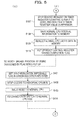
- the switching/resynchronization control circuit 14 starts by being triggered by the saving completion flag being set in the reset control register 18.
- the switching/resynchronization control circuit 14 carries out the operation in and after S201 in ⁇ of FIGS. 4A and 4B on condition that the resynchronization possibility flag with the value indicating that the resynchronization is impossible (the flag 0 in the heretofore described example) is not set in the resynchronization control register 19.
- the switching/resynchronization control circuit 14 carries out the operation in and after S401 depicted in ⁇ of FIG. 5 .
- the switching/resynchronization control circuit 14 sets the clock control circuits 23 and 23 in such a way as to supply clocks to both CPU bus0 7 and CPU bus1 7.
- the switching/resynchronization control circuit 14 issues a reset to each CPU0 6 and CPU1 6 in the system board 1. With the reset, the contents in the memory are held as they are.
- Each CPU0 6 and CPU1 6 reset as a result of the reset issue in S202 reads the firmware stored in the firmware hub 15, and starts the reset firmware process depicted in ⁇ of FIGS. 4A and 4B . Then, in a first S301 after the start, the CPU 6 checks whether or not the synchronization impossible flag is set in the error indication register 20. Then, if the synchronization impossible flag is set, the CPU 6 causes the process to proceed to S310, but if the synchronization impossible flag is not set, the CPU 6 causes the process to proceed to S302. In the event that the switching/resynchronization control circuit 14 issues a reset by executing S202, the synchronization impossible flag is not set, meaning that the process in and after S302 is executed.
- the process in and after S310 will be described after a description of FIG. 5 is given, as a matter of convenience.
- the CPU 6 starts a restoration of the internal information of the normal CPU saved to the memory 12. Even in the event that a CPU 6 which is a processing subject is the abnormal CPU 6 connected to the abnormal CPU bus 7, as the restoration is carried out using the internal information of the normal CPU 6, it is possible to restore a redundant component with the normal CPU 6.
- the CPU 6, by confirming the record of the error indication register 20, checks whether or not there is a desynchronization after the start of the CPU internal information restoration process in S302. Then, if there is a desynchronization, the CPU 6 causes the process to proceed to S306, while if the CPU internal information restoration process is completed without any desynchronization, it causes the process to proceed to S304.
- the CPU 6 compares the number of resynchronization process executions set in the resynchronization control register 19 and the resynchronization possible upper limit. Then, if the number of executions has reached the resynchronization possible upper limit (S307: yes), the CPU 6 determines that it is impossible to further retry the resynchronization process and, in S309, sets the value indicating that the resynchronization is impossible (for example, the flag 0) in the resynchronization control register 19.
- the CPU 6 determines that it is possible to retry the resynchronization process and, in S308, as well as incrementing one of values of the number of executions recorded in the resynchronization control register 19, sets the value indicating that the resynchronization is possible (for example, the flag 1) in the resynchronization control register 19. Then, in either case, the CPU 6 notifies the switching/resynchronization control circuit 14 that it can execute the operation in and after S002 again.
- the CPU 6 waits for the internal information restoration by means of S302 to be completed in the other CPU 6 which is one of the pair of redundant CPU's. Then, on the CPU internal information restoration process being completed in the other CPU 6 too, both CPU's are restored to the addresses immediately before the synchronization break, so the CPU 6 causes the process to proceed to S305.
- the CPU 6 deactivates the comparison of the timer/maximum timer comparison circuit 161, stops the timer counting of the resynchronization timer register 162, and clears the register value thereof to zero. On completing S305, the CPU 6 can restart a normal process in the redundant CPU (S312).
- the CPU 6 deactivates the comparison of the timer/maximum time comparison circuit 161, stops the timer counting of the resynchronization timer register 162, and clears the register value thereof to zero.
- the CPU 6 saves (copies) the internal information of the normal CPU 6 (which, being a register in the CPU and the like, includes the address immediately before the synchronization break) to the memory 12.
- the internal information of the normal CPU 6 which, being a register in the CPU and the like, includes the address immediately before the synchronization break
- the normal CPU 6 reflects (cache flashes), in the memory, the cache data held inside the normal CPU 6. On a saving of the cache data to the memory 12 being completed, the normal CPU 6 causes the process to proceed to S110.
- the normal CPU 6 sets a saving completion flag corresponding to the normal CPU 6 in the reset control register 18. Subsequently, the normal CPU interrupt firm process executed by the normal CPU goes on standby (goes into an infinite loop).
- the switching/resynchronization control circuit 14 starts by being triggered by the saving completion flag being set in the reset control register 18, and carries out the operation in and after S401 in ⁇ of FIG. 5 on condition that the resynchronization possibility flag with the value indicating that the resynchronization is impossible (the flag 0 in the heretofore described example) is set in the resynchronization control register 19.
- the switching/resynchronization control circuit 14 sets the synchronization impossible flag in the error indication register 20.
- the switching/resynchronization control circuit 14 in order to cut off a clock control over an abnormal bus 7 indicated by the ID of an abnormal CPU bus 7 recorded in the error indication register 20, sets a clock control circuit 23 connected to the abnormal bus 7, and thereby degenerates the abnormal bus 7.
- the switching/resynchronization control circuit 14 as well as issuing a reset only to a normal CPU 6 (that is, a CPU 6 connected to a CPU bus 7 which is not the abnormal CPU bus 7 indicated by the ID recorded in the error indication register 20, that is, to a normal CPU bus 7) in S403, fixes the changeover switch 17 to the normal CPU bus 7 side in S404.
- the normal CPU 6 refers to the error indication register 20, and notifies the system control/management apparatus 5 of the contents of errors set.
- the normal CPU 6 starts restoring the internal information of the normal CPU 6 saved to the memory 12. On this restoration process being completed, the normal CPU 6 can restart the normal process in an independent operation (S312).
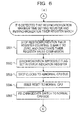
- the timer/maximum timer comparison circuit 161 caused to start the comparison in S101, unless the comparison is deactivated in S107, continues to compare the count value of the resynchronization timer register 162 and the value of the resynchronization upper limit setting register 163. Then, on detecting that the former has reached the latter, the timer/maximum time comparison circuit 161 notifies the switching/resynchronization control circuit 14 of that fact.
- the switching/resynchronization control circuit 14 which has received this notification starts the operation depicted in FIG. 6 by means of an interrupt.
- the switching/resynchronization control circuit 14 in a first S501, deactivates the comparison of the timer/maximum time comparison circuit 161, stops the timer count of the resynchronization timer register 162, and clears the register value thereof to zero.
- the switching/resynchronization control circuit 14 sets the synchronization impossible flag in the error indication register 20.
- the switching/resynchronization control circuit 14 in order to cut off a clock control over an abnormal bus 7 indicated by the ID of an abnormal CPU bus 7 recorded in the error indication register 20, sets a clock control circuit 23 connected to the abnormal bus 7, and thereby degenerates the abnormal bus 7.
- the switching/resynchronization control circuit 14 as well as issuing a reset only to a normal CPU 6 (that is, a CPU 6 connected to a CPU bus 7 which is not the abnormal CPU bus 7 indicated by the ID recorded in the error indication register 20, that is, to a normal CPU bus 7) in S504, fixes the changeover switch 17 to the normal CPU bus 7 side in S505.
- the normal CPU 6 refers to the error indication register 20, and notifies the system control/management apparatus 5 of the contents of errors set.
- the normal CPU 6 starts restoring the internal information of the normal CPU 6 saved to the memory 12. On this restoration process being completed, the normal CPU 6 can restart the normal process in an independent operation (S312).
- the various features may be implemented in hardware, or as software modules running on one or more processors. Features of one aspect may be applied to any of the other aspects.
- the invention also provides a computer program or a computer program product for carrying out any of the methods described herein, and a computer readable medium having stored thereon a program for carrying out any of the methods described herein.
- a computer program embodying the invention may be stored on a computer-readable medium, or it could, for example, be in the form of a signal such as a downloadable data signal provided from an Internet website, or it could be in any other form.
Applications Claiming Priority (1)
| Application Number | Priority Date | Filing Date | Title |
|---|---|---|---|
| JP2008258728A JP5347414B2 (ja) | 2008-10-03 | 2008-10-03 | 同期制御装置,情報処理装置及び同期管理方法 |
Publications (2)
| Publication Number | Publication Date |
|---|---|
| EP2175371A1 true EP2175371A1 (fr) | 2010-04-14 |
| EP2175371B1 EP2175371B1 (fr) | 2015-03-18 |
Family
ID=41360116
Family Applications (1)
| Application Number | Title | Priority Date | Filing Date |
|---|---|---|---|
| EP09170690.3A Not-in-force EP2175371B1 (fr) | 2008-10-03 | 2009-09-18 | Appareils de contrôle de synchronisation, appareils de traitement d'informations, et procédés de gestion de synchronisation |
Country Status (5)
| Country | Link |
|---|---|
| US (1) | US8667315B2 (fr) |
| EP (1) | EP2175371B1 (fr) |
| JP (1) | JP5347414B2 (fr) |
| KR (1) | KR101121116B1 (fr) |
| CN (1) | CN101714108B (fr) |
Cited By (3)
| Publication number | Priority date | Publication date | Assignee | Title |
|---|---|---|---|---|
| WO2013174490A1 (fr) | 2012-05-24 | 2013-11-28 | Phoenix Contact Gmbh & Co. Kg | Circuit d'entrée de signaux analogiques avec un certain nombre de canaux de détection de signaux analogiques |
| EP3486780A1 (fr) * | 2017-11-21 | 2019-05-22 | The Boeing Company | Système d'alignement de traitement d'instructions |
| US10599513B2 (en) | 2017-11-21 | 2020-03-24 | The Boeing Company | Message synchronization system |
Families Citing this family (11)
| Publication number | Priority date | Publication date | Assignee | Title |
|---|---|---|---|---|
| DE102009050161A1 (de) * | 2009-10-21 | 2011-04-28 | Siemens Aktiengesellschaft | Verfahren und Vorrichtung zum Testen eines Systems mit zumindest einer Mehrzahl von parallel ausführbaren Softwareeinheiten |
| CN102469474A (zh) * | 2010-11-15 | 2012-05-23 | 中兴通讯股份有限公司 | 一种通信设备异常信息的处理方法及装置 |
| CN102043690A (zh) * | 2010-12-31 | 2011-05-04 | 上海华为技术有限公司 | 多核处理器故障处理方法及多核处理器 |
| JP5601353B2 (ja) * | 2012-06-29 | 2014-10-08 | 横河電機株式会社 | ネットワーク管理システム |
| JP6050083B2 (ja) * | 2012-10-18 | 2016-12-21 | ルネサスエレクトロニクス株式会社 | 半導体装置 |
| TWI571712B (zh) * | 2015-10-29 | 2017-02-21 | 行政院原子能委員會核能研究所 | 多重容錯控制系統及其同步方法 |
| JP6729407B2 (ja) * | 2017-01-13 | 2020-07-22 | 株式会社デンソー | マイクロコンピュータ |
| FR3071688B1 (fr) | 2017-09-22 | 2019-09-27 | Thales | Procede de syncronisation d'un ensemble de dispositifs, programme d'ordinateur et systeme de syncronisation associes |
| JP7298442B2 (ja) * | 2019-10-25 | 2023-06-27 | 株式会社リコー | 電子制御装置、電子制御装置のメインプロセッサによる制御方法および電子制御装置のメインプロセッサが実行する制御プログラム |
| CN113050752B (zh) * | 2021-03-29 | 2023-02-21 | 中车青岛四方车辆研究所有限公司 | 用于两个中央处理器时间同步的方法和存储介质 |
| CN113886039B (zh) * | 2021-09-18 | 2023-12-22 | 中汽创智科技有限公司 | 一种调度表同步方法、装置、电子设备及存储介质 |
Citations (8)
| Publication number | Priority date | Publication date | Assignee | Title |
|---|---|---|---|---|
| US4358823A (en) * | 1977-03-25 | 1982-11-09 | Trw, Inc. | Double redundant processor |
| GB2268817A (en) * | 1992-07-17 | 1994-01-19 | Integrated Micro Products Ltd | Fault-tolerant computer system |
| US5748873A (en) * | 1992-09-17 | 1998-05-05 | Hitachi,Ltd. | Fault recovering system provided in highly reliable computer system having duplicated processors |
| US6393582B1 (en) | 1998-12-10 | 2002-05-21 | Compaq Computer Corporation | Error self-checking and recovery using lock-step processor pair architecture |
| EP1380953A1 (fr) | 2002-07-12 | 2004-01-14 | Nec Corporation | Machine informatique à tolérance de fautes, son procédé de resynchronisation et logiciel de resynchronisation correspondant |
| JP2005285119A (ja) | 2004-03-30 | 2005-10-13 | Hewlett-Packard Development Co Lp | 非決定的プロセッサにおいてユーザプログラムを実行する方法およびシステム |
| EP1675003A2 (fr) | 2004-12-21 | 2006-06-28 | NEC Corporation | Système et contrôleur à tolérance de pannes, procédé de fonctionnement, et programme de fonctionnement utilisé dans le système à tolérance de pannes |
| JP2006302289A (ja) | 2005-04-19 | 2006-11-02 | Hewlett-Packard Development Co Lp | ロックステップ及びフリーステップの両プロセッサモードによる計算処理 |
Family Cites Families (7)
| Publication number | Priority date | Publication date | Assignee | Title |
|---|---|---|---|---|
| GB1253309A (en) * | 1969-11-21 | 1971-11-10 | Marconi Co Ltd | Improvements in or relating to data processing arrangements |
| US3810119A (en) * | 1971-05-04 | 1974-05-07 | Us Navy | Processor synchronization scheme |
| US4490561A (en) * | 1983-10-13 | 1984-12-25 | Conoco Inc. | Method for alkoxylating fluorinated alcohols |
| AU616213B2 (en) * | 1987-11-09 | 1991-10-24 | Tandem Computers Incorporated | Method and apparatus for synchronizing a plurality of processors |
| JPH0630094B2 (ja) * | 1989-03-13 | 1994-04-20 | インターナショナル・ビジネス・マシーンズ・コーポレイション | マルチプロセツサ・システム |
| JP4117684B2 (ja) * | 2004-12-20 | 2008-07-16 | 日本電気株式会社 | フォルトトレラント・二重化コンピュータシステムとその制御方法 |
| JP5013309B2 (ja) * | 2006-08-18 | 2012-08-29 | 日本電気株式会社 | フォールトトレラントコンピュータ、そのトランザクション同期制御方法 |
-
2008
- 2008-10-03 JP JP2008258728A patent/JP5347414B2/ja active Active
-
2009
- 2009-09-18 EP EP09170690.3A patent/EP2175371B1/fr not_active Not-in-force
- 2009-09-29 US US12/569,333 patent/US8667315B2/en not_active Expired - Fee Related
- 2009-09-30 CN CN200910177655.5A patent/CN101714108B/zh not_active Expired - Fee Related
- 2009-10-01 KR KR1020090093924A patent/KR101121116B1/ko not_active IP Right Cessation
Patent Citations (8)
| Publication number | Priority date | Publication date | Assignee | Title |
|---|---|---|---|---|
| US4358823A (en) * | 1977-03-25 | 1982-11-09 | Trw, Inc. | Double redundant processor |
| GB2268817A (en) * | 1992-07-17 | 1994-01-19 | Integrated Micro Products Ltd | Fault-tolerant computer system |
| US5748873A (en) * | 1992-09-17 | 1998-05-05 | Hitachi,Ltd. | Fault recovering system provided in highly reliable computer system having duplicated processors |
| US6393582B1 (en) | 1998-12-10 | 2002-05-21 | Compaq Computer Corporation | Error self-checking and recovery using lock-step processor pair architecture |
| EP1380953A1 (fr) | 2002-07-12 | 2004-01-14 | Nec Corporation | Machine informatique à tolérance de fautes, son procédé de resynchronisation et logiciel de resynchronisation correspondant |
| JP2005285119A (ja) | 2004-03-30 | 2005-10-13 | Hewlett-Packard Development Co Lp | 非決定的プロセッサにおいてユーザプログラムを実行する方法およびシステム |
| EP1675003A2 (fr) | 2004-12-21 | 2006-06-28 | NEC Corporation | Système et contrôleur à tolérance de pannes, procédé de fonctionnement, et programme de fonctionnement utilisé dans le système à tolérance de pannes |
| JP2006302289A (ja) | 2005-04-19 | 2006-11-02 | Hewlett-Packard Development Co Lp | ロックステップ及びフリーステップの両プロセッサモードによる計算処理 |
Non-Patent Citations (2)
| Title |
|---|
| JONES D: "FEHLERTOLERANZ UND ZUVERLAESSIGKEIT IN MIKROPROZESSOR-SYSTEMEN. \AM BEISPIEL DER FAMILIE MC88000", ELEKTRONIK, WEKA FACHZEITSCHRIFTENVERLAG, POING, DE, vol. 39, no. 24, 23 November 1990 (1990-11-23), pages 54 - 60, XP000172269, ISSN: 0013-5658 * |
| ROLUND M W ED - NATIONAL ENGINEERING CONSORTIUM: "FAULT TOLERANT DESIGNS", PROCEEDINGS OF THE NATIONAL COMMUNICATIONS FORUM. ROSEMONT, OCT. 7 - 9, 1985, CHICAGO, NEC, US, vol. 39, 1 October 1985 (1985-10-01), pages 735 - 738, XP000744730 * |
Cited By (6)
| Publication number | Priority date | Publication date | Assignee | Title |
|---|---|---|---|---|
| WO2013174490A1 (fr) | 2012-05-24 | 2013-11-28 | Phoenix Contact Gmbh & Co. Kg | Circuit d'entrée de signaux analogiques avec un certain nombre de canaux de détection de signaux analogiques |
| US9658267B2 (en) | 2012-05-24 | 2017-05-23 | Phoenix Contact Gmbh & Co. Kg | Analog signal input circuit to process analog input signals for the safety of a process |
| EP3486780A1 (fr) * | 2017-11-21 | 2019-05-22 | The Boeing Company | Système d'alignement de traitement d'instructions |
| JP2019125350A (ja) * | 2017-11-21 | 2019-07-25 | ザ・ボーイング・カンパニーThe Boeing Company | 指示命令処理調節システム |
| US10528077B2 (en) | 2017-11-21 | 2020-01-07 | The Boeing Company | Instruction processing alignment system |
| US10599513B2 (en) | 2017-11-21 | 2020-03-24 | The Boeing Company | Message synchronization system |
Also Published As
| Publication number | Publication date |
|---|---|
| US8667315B2 (en) | 2014-03-04 |
| KR101121116B1 (ko) | 2012-03-20 |
| KR20100038159A (ko) | 2010-04-13 |
| CN101714108B (zh) | 2014-05-07 |
| JP5347414B2 (ja) | 2013-11-20 |
| CN101714108A (zh) | 2010-05-26 |
| JP2010092105A (ja) | 2010-04-22 |
| EP2175371B1 (fr) | 2015-03-18 |
| US20100088535A1 (en) | 2010-04-08 |
Similar Documents
| Publication | Publication Date | Title |
|---|---|---|
| EP2175371B1 (fr) | Appareils de contrôle de synchronisation, appareils de traitement d'informations, et procédés de gestion de synchronisation | |
| US7496786B2 (en) | Systems and methods for maintaining lock step operation | |
| US9582448B2 (en) | Transmission apparatus and control unit | |
| US9195553B2 (en) | Redundant system control method | |
| CA2032067A1 (fr) | Systeme informatique insensible aux defaillances a re-integration et a relance en direct | |
| KR101581608B1 (ko) | 프로세서 시스템 | |
| JP3030658B2 (ja) | 電源故障対策を備えたコンピュータシステム及びその動作方法 | |
| JPH0950424A (ja) | ダンプ採取装置およびダンプ採取方法 | |
| JP5287974B2 (ja) | 演算処理システム、再同期方法、およびファームプログラム | |
| US20040193735A1 (en) | Method and circuit arrangement for synchronization of synchronously or asynchronously clocked processor units | |
| JP2006178659A (ja) | フォールト・トレラント・コンピュータシステムと、そのための割り込み制御方法 | |
| US8181064B2 (en) | Information processing apparatus for inhibiting instructions, saving and restoring internal information in response to abnormality in redundant processor system | |
| JP2008015704A (ja) | マルチプロセッサシステム | |
| JP2003256240A (ja) | 情報処理装置及びその障害回復方法 | |
| WO2014112039A1 (fr) | Dispositif de traitement d'informations, procédé de commande de dispositif de traitement d'informations et programme de commande de dispositif de traitement d'informations | |
| JPH05216855A (ja) | マルチcpu制御方式 | |
| JP2004013723A (ja) | 共有メモリを使ったクラスタ構成を採用した情報処理システムの障害処理装置と方法 | |
| JP4973755B2 (ja) | ストール監視装置、ストール監視方法及びプログラム | |
| JP2000347758A (ja) | 情報処理装置 | |
| JPH04211841A (ja) | 二重化処理装置 | |
| WO2016194170A1 (fr) | Dispositif de détection d'erreur et système de détection d'erreur | |
| JP2011210074A (ja) | メモリ情報採取システム、メモリ情報採取方法、メモリ情報採取プログラムおよびプログラム記憶媒体 | |
| JP2000298619A (ja) | キャッシュメモリの障害処理方式 | |
| JPH0594326A (ja) | バス障害検出時のアダプタ処理方式 |
Legal Events
| Date | Code | Title | Description |
|---|---|---|---|
| PUAI | Public reference made under article 153(3) epc to a published international application that has entered the european phase |
Free format text: ORIGINAL CODE: 0009012 |
|
| AK | Designated contracting states |
Kind code of ref document: A1 Designated state(s): AT BE BG CH CY CZ DE DK EE ES FI FR GB GR HR HU IE IS IT LI LT LU LV MC MK MT NL NO PL PT RO SE SI SK SM TR |
|
| AX | Request for extension of the european patent |
Extension state: AL BA RS |
|
| 17P | Request for examination filed |
Effective date: 20101013 |
|
| 17Q | First examination report despatched |
Effective date: 20101108 |
|
| GRAP | Despatch of communication of intention to grant a patent |
Free format text: ORIGINAL CODE: EPIDOSNIGR1 |
|
| INTG | Intention to grant announced |
Effective date: 20141006 |
|
| GRAS | Grant fee paid |
Free format text: ORIGINAL CODE: EPIDOSNIGR3 |
|
| GRAA | (expected) grant |
Free format text: ORIGINAL CODE: 0009210 |
|
| AK | Designated contracting states |
Kind code of ref document: B1 Designated state(s): AT BE BG CH CY CZ DE DK EE ES FI FR GB GR HR HU IE IS IT LI LT LU LV MC MK MT NL NO PL PT RO SE SI SK SM TR |
|
| REG | Reference to a national code |
Ref country code: GB Ref legal event code: FG4D |
|
| REG | Reference to a national code |
Ref country code: CH Ref legal event code: EP |
|
| REG | Reference to a national code |
Ref country code: IE Ref legal event code: FG4D |
|
| REG | Reference to a national code |
Ref country code: AT Ref legal event code: REF Ref document number: 716972 Country of ref document: AT Kind code of ref document: T Effective date: 20150415 |
|
| REG | Reference to a national code |
Ref country code: DE Ref legal event code: R096 Ref document number: 602009030015 Country of ref document: DE Effective date: 20150430 |
|
| REG | Reference to a national code |
Ref country code: NL Ref legal event code: VDEP Effective date: 20150318 |
|
| REG | Reference to a national code |
Ref country code: NL Ref legal event code: VDEP Effective date: 20150318 |
|
| PG25 | Lapsed in a contracting state [announced via postgrant information from national office to epo] |
Ref country code: FI Free format text: LAPSE BECAUSE OF FAILURE TO SUBMIT A TRANSLATION OF THE DESCRIPTION OR TO PAY THE FEE WITHIN THE PRESCRIBED TIME-LIMIT Effective date: 20150318 Ref country code: HR Free format text: LAPSE BECAUSE OF FAILURE TO SUBMIT A TRANSLATION OF THE DESCRIPTION OR TO PAY THE FEE WITHIN THE PRESCRIBED TIME-LIMIT Effective date: 20150318 Ref country code: LT Free format text: LAPSE BECAUSE OF FAILURE TO SUBMIT A TRANSLATION OF THE DESCRIPTION OR TO PAY THE FEE WITHIN THE PRESCRIBED TIME-LIMIT Effective date: 20150318 Ref country code: NO Free format text: LAPSE BECAUSE OF FAILURE TO SUBMIT A TRANSLATION OF THE DESCRIPTION OR TO PAY THE FEE WITHIN THE PRESCRIBED TIME-LIMIT Effective date: 20150618 Ref country code: SE Free format text: LAPSE BECAUSE OF FAILURE TO SUBMIT A TRANSLATION OF THE DESCRIPTION OR TO PAY THE FEE WITHIN THE PRESCRIBED TIME-LIMIT Effective date: 20150318 |
|
| REG | Reference to a national code |
Ref country code: AT Ref legal event code: MK05 Ref document number: 716972 Country of ref document: AT Kind code of ref document: T Effective date: 20150318 |
|
| REG | Reference to a national code |
Ref country code: LT Ref legal event code: MG4D |
|
| PG25 | Lapsed in a contracting state [announced via postgrant information from national office to epo] |
Ref country code: GR Free format text: LAPSE BECAUSE OF FAILURE TO SUBMIT A TRANSLATION OF THE DESCRIPTION OR TO PAY THE FEE WITHIN THE PRESCRIBED TIME-LIMIT Effective date: 20150619 Ref country code: LV Free format text: LAPSE BECAUSE OF FAILURE TO SUBMIT A TRANSLATION OF THE DESCRIPTION OR TO PAY THE FEE WITHIN THE PRESCRIBED TIME-LIMIT Effective date: 20150318 |
|
| PG25 | Lapsed in a contracting state [announced via postgrant information from national office to epo] |
Ref country code: NL Free format text: LAPSE BECAUSE OF FAILURE TO SUBMIT A TRANSLATION OF THE DESCRIPTION OR TO PAY THE FEE WITHIN THE PRESCRIBED TIME-LIMIT Effective date: 20150318 |
|
| PG25 | Lapsed in a contracting state [announced via postgrant information from national office to epo] |
Ref country code: EE Free format text: LAPSE BECAUSE OF FAILURE TO SUBMIT A TRANSLATION OF THE DESCRIPTION OR TO PAY THE FEE WITHIN THE PRESCRIBED TIME-LIMIT Effective date: 20150318 Ref country code: SK Free format text: LAPSE BECAUSE OF FAILURE TO SUBMIT A TRANSLATION OF THE DESCRIPTION OR TO PAY THE FEE WITHIN THE PRESCRIBED TIME-LIMIT Effective date: 20150318 Ref country code: PT Free format text: LAPSE BECAUSE OF FAILURE TO SUBMIT A TRANSLATION OF THE DESCRIPTION OR TO PAY THE FEE WITHIN THE PRESCRIBED TIME-LIMIT Effective date: 20150720 Ref country code: RO Free format text: LAPSE BECAUSE OF FAILURE TO SUBMIT A TRANSLATION OF THE DESCRIPTION OR TO PAY THE FEE WITHIN THE PRESCRIBED TIME-LIMIT Effective date: 20150318 Ref country code: CZ Free format text: LAPSE BECAUSE OF FAILURE TO SUBMIT A TRANSLATION OF THE DESCRIPTION OR TO PAY THE FEE WITHIN THE PRESCRIBED TIME-LIMIT Effective date: 20150318 Ref country code: ES Free format text: LAPSE BECAUSE OF FAILURE TO SUBMIT A TRANSLATION OF THE DESCRIPTION OR TO PAY THE FEE WITHIN THE PRESCRIBED TIME-LIMIT Effective date: 20150318 |
|
| PG25 | Lapsed in a contracting state [announced via postgrant information from national office to epo] |
Ref country code: IS Free format text: LAPSE BECAUSE OF FAILURE TO SUBMIT A TRANSLATION OF THE DESCRIPTION OR TO PAY THE FEE WITHIN THE PRESCRIBED TIME-LIMIT Effective date: 20150718 Ref country code: PL Free format text: LAPSE BECAUSE OF FAILURE TO SUBMIT A TRANSLATION OF THE DESCRIPTION OR TO PAY THE FEE WITHIN THE PRESCRIBED TIME-LIMIT Effective date: 20150318 Ref country code: AT Free format text: LAPSE BECAUSE OF FAILURE TO SUBMIT A TRANSLATION OF THE DESCRIPTION OR TO PAY THE FEE WITHIN THE PRESCRIBED TIME-LIMIT Effective date: 20150318 |
|
| REG | Reference to a national code |
Ref country code: DE Ref legal event code: R097 Ref document number: 602009030015 Country of ref document: DE |
|
| PG25 | Lapsed in a contracting state [announced via postgrant information from national office to epo] |
Ref country code: IT Free format text: LAPSE BECAUSE OF FAILURE TO SUBMIT A TRANSLATION OF THE DESCRIPTION OR TO PAY THE FEE WITHIN THE PRESCRIBED TIME-LIMIT Effective date: 20150318 |
|
| PLBE | No opposition filed within time limit |
Free format text: ORIGINAL CODE: 0009261 |
|
| STAA | Information on the status of an ep patent application or granted ep patent |
Free format text: STATUS: NO OPPOSITION FILED WITHIN TIME LIMIT |
|
| PG25 | Lapsed in a contracting state [announced via postgrant information from national office to epo] |
Ref country code: DK Free format text: LAPSE BECAUSE OF FAILURE TO SUBMIT A TRANSLATION OF THE DESCRIPTION OR TO PAY THE FEE WITHIN THE PRESCRIBED TIME-LIMIT Effective date: 20150318 |
|
| 26N | No opposition filed |
Effective date: 20151221 |
|
| PG25 | Lapsed in a contracting state [announced via postgrant information from national office to epo] |
Ref country code: SI Free format text: LAPSE BECAUSE OF FAILURE TO SUBMIT A TRANSLATION OF THE DESCRIPTION OR TO PAY THE FEE WITHIN THE PRESCRIBED TIME-LIMIT Effective date: 20150318 |
|
| PG25 | Lapsed in a contracting state [announced via postgrant information from national office to epo] |
Ref country code: LU Free format text: LAPSE BECAUSE OF FAILURE TO SUBMIT A TRANSLATION OF THE DESCRIPTION OR TO PAY THE FEE WITHIN THE PRESCRIBED TIME-LIMIT Effective date: 20150918 Ref country code: MC Free format text: LAPSE BECAUSE OF FAILURE TO SUBMIT A TRANSLATION OF THE DESCRIPTION OR TO PAY THE FEE WITHIN THE PRESCRIBED TIME-LIMIT Effective date: 20150318 |
|
| REG | Reference to a national code |
Ref country code: CH Ref legal event code: PL |
|
| REG | Reference to a national code |
Ref country code: IE Ref legal event code: MM4A |
|
| PG25 | Lapsed in a contracting state [announced via postgrant information from national office to epo] |
Ref country code: CH Free format text: LAPSE BECAUSE OF NON-PAYMENT OF DUE FEES Effective date: 20150930 Ref country code: LI Free format text: LAPSE BECAUSE OF NON-PAYMENT OF DUE FEES Effective date: 20150930 Ref country code: IE Free format text: LAPSE BECAUSE OF NON-PAYMENT OF DUE FEES Effective date: 20150918 |
|
| REG | Reference to a national code |
Ref country code: FR Ref legal event code: PLFP Year of fee payment: 8 |
|
| PG25 | Lapsed in a contracting state [announced via postgrant information from national office to epo] |
Ref country code: BE Free format text: LAPSE BECAUSE OF FAILURE TO SUBMIT A TRANSLATION OF THE DESCRIPTION OR TO PAY THE FEE WITHIN THE PRESCRIBED TIME-LIMIT Effective date: 20150318 |
|
| PG25 | Lapsed in a contracting state [announced via postgrant information from national office to epo] |
Ref country code: MT Free format text: LAPSE BECAUSE OF FAILURE TO SUBMIT A TRANSLATION OF THE DESCRIPTION OR TO PAY THE FEE WITHIN THE PRESCRIBED TIME-LIMIT Effective date: 20150318 |
|
| PG25 | Lapsed in a contracting state [announced via postgrant information from national office to epo] |
Ref country code: HU Free format text: LAPSE BECAUSE OF FAILURE TO SUBMIT A TRANSLATION OF THE DESCRIPTION OR TO PAY THE FEE WITHIN THE PRESCRIBED TIME-LIMIT; INVALID AB INITIO Effective date: 20090918 Ref country code: BG Free format text: LAPSE BECAUSE OF FAILURE TO SUBMIT A TRANSLATION OF THE DESCRIPTION OR TO PAY THE FEE WITHIN THE PRESCRIBED TIME-LIMIT Effective date: 20150318 Ref country code: SM Free format text: LAPSE BECAUSE OF FAILURE TO SUBMIT A TRANSLATION OF THE DESCRIPTION OR TO PAY THE FEE WITHIN THE PRESCRIBED TIME-LIMIT Effective date: 20150318 |
|
| PG25 | Lapsed in a contracting state [announced via postgrant information from national office to epo] |
Ref country code: CY Free format text: LAPSE BECAUSE OF FAILURE TO SUBMIT A TRANSLATION OF THE DESCRIPTION OR TO PAY THE FEE WITHIN THE PRESCRIBED TIME-LIMIT Effective date: 20150318 |
|
| REG | Reference to a national code |
Ref country code: FR Ref legal event code: PLFP Year of fee payment: 9 |
|
| PG25 | Lapsed in a contracting state [announced via postgrant information from national office to epo] |
Ref country code: TR Free format text: LAPSE BECAUSE OF FAILURE TO SUBMIT A TRANSLATION OF THE DESCRIPTION OR TO PAY THE FEE WITHIN THE PRESCRIBED TIME-LIMIT Effective date: 20150318 |
|
| PGFP | Annual fee paid to national office [announced via postgrant information from national office to epo] |
Ref country code: GB Payment date: 20170913 Year of fee payment: 9 Ref country code: DE Payment date: 20170912 Year of fee payment: 9 Ref country code: FR Payment date: 20170810 Year of fee payment: 9 |
|
| PG25 | Lapsed in a contracting state [announced via postgrant information from national office to epo] |
Ref country code: MK Free format text: LAPSE BECAUSE OF FAILURE TO SUBMIT A TRANSLATION OF THE DESCRIPTION OR TO PAY THE FEE WITHIN THE PRESCRIBED TIME-LIMIT Effective date: 20150318 |
|
| REG | Reference to a national code |
Ref country code: DE Ref legal event code: R119 Ref document number: 602009030015 Country of ref document: DE |
|
| GBPC | Gb: european patent ceased through non-payment of renewal fee |
Effective date: 20180918 |
|
| PG25 | Lapsed in a contracting state [announced via postgrant information from national office to epo] |
Ref country code: DE Free format text: LAPSE BECAUSE OF NON-PAYMENT OF DUE FEES Effective date: 20190402 |
|
| PG25 | Lapsed in a contracting state [announced via postgrant information from national office to epo] |
Ref country code: FR Free format text: LAPSE BECAUSE OF NON-PAYMENT OF DUE FEES Effective date: 20180930 |
|
| PG25 | Lapsed in a contracting state [announced via postgrant information from national office to epo] |
Ref country code: GB Free format text: LAPSE BECAUSE OF NON-PAYMENT OF DUE FEES Effective date: 20180918 |