EP2160640B1 - Optisches modul - Google Patents
Optisches modul Download PDFInfo
- Publication number
- EP2160640B1 EP2160640B1 EP08765872.0A EP08765872A EP2160640B1 EP 2160640 B1 EP2160640 B1 EP 2160640B1 EP 08765872 A EP08765872 A EP 08765872A EP 2160640 B1 EP2160640 B1 EP 2160640B1
- Authority
- EP
- European Patent Office
- Prior art keywords
- mounting substrate
- substrate
- external waveguide
- core
- adhesive
- Prior art date
- Legal status (The legal status is an assumption and is not a legal conclusion. Google has not performed a legal analysis and makes no representation as to the accuracy of the status listed.)
- Not-in-force
Links
- 230000003287 optical effect Effects 0.000 title claims description 161
- 239000000758 substrate Substances 0.000 claims description 932
- 239000000853 adhesive Substances 0.000 claims description 313
- 230000001070 adhesive effect Effects 0.000 claims description 313
- 230000013011 mating Effects 0.000 claims description 139
- 230000007246 mechanism Effects 0.000 claims description 93
- 239000000463 material Substances 0.000 claims description 51
- 230000008878 coupling Effects 0.000 claims description 17
- 238000010168 coupling process Methods 0.000 claims description 17
- 238000005859 coupling reaction Methods 0.000 claims description 17
- 239000011162 core material Substances 0.000 description 279
- 238000005253 cladding Methods 0.000 description 68
- 239000010410 layer Substances 0.000 description 29
- 238000000034 method Methods 0.000 description 26
- 238000004026 adhesive bonding Methods 0.000 description 22
- 229920000642 polymer Polymers 0.000 description 19
- 230000005540 biological transmission Effects 0.000 description 12
- 230000009467 reduction Effects 0.000 description 11
- 239000012790 adhesive layer Substances 0.000 description 10
- 230000009471 action Effects 0.000 description 9
- XUIMIQQOPSSXEZ-UHFFFAOYSA-N Silicon Chemical compound [Si] XUIMIQQOPSSXEZ-UHFFFAOYSA-N 0.000 description 8
- 229910052710 silicon Inorganic materials 0.000 description 8
- 239000010703 silicon Substances 0.000 description 8
- 230000000694 effects Effects 0.000 description 7
- 238000004519 manufacturing process Methods 0.000 description 7
- 230000008569 process Effects 0.000 description 7
- 230000015572 biosynthetic process Effects 0.000 description 6
- 238000005304 joining Methods 0.000 description 6
- 239000004033 plastic Substances 0.000 description 6
- 229920003023 plastic Polymers 0.000 description 6
- 239000004593 Epoxy Substances 0.000 description 5
- 238000005520 cutting process Methods 0.000 description 4
- 230000001902 propagating effect Effects 0.000 description 4
- 238000004873 anchoring Methods 0.000 description 3
- 238000005530 etching Methods 0.000 description 3
- 239000000835 fiber Substances 0.000 description 3
- 238000001020 plasma etching Methods 0.000 description 3
- 239000004065 semiconductor Substances 0.000 description 3
- 238000004528 spin coating Methods 0.000 description 3
- 230000035882 stress Effects 0.000 description 3
- 229920001187 thermosetting polymer Polymers 0.000 description 3
- 238000000151 deposition Methods 0.000 description 2
- 238000010586 diagram Methods 0.000 description 2
- 238000001312 dry etching Methods 0.000 description 2
- 238000004049 embossing Methods 0.000 description 2
- 229920006332 epoxy adhesive Polymers 0.000 description 2
- 239000003822 epoxy resin Substances 0.000 description 2
- 238000002474 experimental method Methods 0.000 description 2
- PCHJSUWPFVWCPO-UHFFFAOYSA-N gold Chemical compound [Au] PCHJSUWPFVWCPO-UHFFFAOYSA-N 0.000 description 2
- 229910052737 gold Inorganic materials 0.000 description 2
- 239000010931 gold Substances 0.000 description 2
- 230000001678 irradiating effect Effects 0.000 description 2
- 229920000647 polyepoxide Polymers 0.000 description 2
- 229920000139 polyethylene terephthalate Polymers 0.000 description 2
- 239000005020 polyethylene terephthalate Substances 0.000 description 2
- 229920001296 polysiloxane Polymers 0.000 description 2
- 238000012545 processing Methods 0.000 description 2
- 229920005989 resin Polymers 0.000 description 2
- 239000011347 resin Substances 0.000 description 2
- JBRZTFJDHDCESZ-UHFFFAOYSA-N AsGa Chemical compound [As]#[Ga] JBRZTFJDHDCESZ-UHFFFAOYSA-N 0.000 description 1
- 241001481828 Glyptocephalus cynoglossus Species 0.000 description 1
- KWYUFKZDYYNOTN-UHFFFAOYSA-M Potassium hydroxide Chemical compound [OH-].[K+] KWYUFKZDYYNOTN-UHFFFAOYSA-M 0.000 description 1
- NIXOWILDQLNWCW-UHFFFAOYSA-N acrylic acid group Chemical group C(C=C)(=O)O NIXOWILDQLNWCW-UHFFFAOYSA-N 0.000 description 1
- 229910052782 aluminium Inorganic materials 0.000 description 1
- XAGFODPZIPBFFR-UHFFFAOYSA-N aluminium Chemical compound [Al] XAGFODPZIPBFFR-UHFFFAOYSA-N 0.000 description 1
- QVGXLLKOCUKJST-UHFFFAOYSA-N atomic oxygen Chemical compound [O] QVGXLLKOCUKJST-UHFFFAOYSA-N 0.000 description 1
- 238000005452 bending Methods 0.000 description 1
- 230000008901 benefit Effects 0.000 description 1
- 239000000919 ceramic Substances 0.000 description 1
- 238000003486 chemical etching Methods 0.000 description 1
- 239000011248 coating agent Substances 0.000 description 1
- 238000000576 coating method Methods 0.000 description 1
- 150000001875 compounds Chemical class 0.000 description 1
- 230000007423 decrease Effects 0.000 description 1
- 238000013461 design Methods 0.000 description 1
- 230000006866 deterioration Effects 0.000 description 1
- 238000011161 development Methods 0.000 description 1
- 238000006073 displacement reaction Methods 0.000 description 1
- 238000001704 evaporation Methods 0.000 description 1
- 230000006355 external stress Effects 0.000 description 1
- 238000005429 filling process Methods 0.000 description 1
- 239000012634 fragment Substances 0.000 description 1
- 239000011521 glass Substances 0.000 description 1
- 230000001788 irregular Effects 0.000 description 1
- 239000013307 optical fiber Substances 0.000 description 1
- 229910052760 oxygen Inorganic materials 0.000 description 1
- 239000001301 oxygen Substances 0.000 description 1
- 238000000059 patterning Methods 0.000 description 1
- -1 polyethylene terephthalate Polymers 0.000 description 1
- 229920001721 polyimide Polymers 0.000 description 1
- 238000007788 roughening Methods 0.000 description 1
- 229920002050 silicone resin Polymers 0.000 description 1
- 238000000992 sputter etching Methods 0.000 description 1
- 238000011144 upstream manufacturing Methods 0.000 description 1
Images












Classifications
-
- G—PHYSICS
- G02—OPTICS
- G02B—OPTICAL ELEMENTS, SYSTEMS OR APPARATUS
- G02B6/00—Light guides; Structural details of arrangements comprising light guides and other optical elements, e.g. couplings
- G02B6/24—Coupling light guides
- G02B6/26—Optical coupling means
-
- G—PHYSICS
- G02—OPTICS
- G02B—OPTICAL ELEMENTS, SYSTEMS OR APPARATUS
- G02B6/00—Light guides; Structural details of arrangements comprising light guides and other optical elements, e.g. couplings
- G02B6/24—Coupling light guides
- G02B6/42—Coupling light guides with opto-electronic elements
- G02B6/4201—Packages, e.g. shape, construction, internal or external details
- G02B6/4219—Mechanical fixtures for holding or positioning the elements relative to each other in the couplings; Alignment methods for the elements, e.g. measuring or observing methods especially used therefor
- G02B6/4228—Passive alignment, i.e. without a detection of the degree of coupling or the position of the elements
- G02B6/423—Passive alignment, i.e. without a detection of the degree of coupling or the position of the elements using guiding surfaces for the alignment
-
- G—PHYSICS
- G02—OPTICS
- G02B—OPTICAL ELEMENTS, SYSTEMS OR APPARATUS
- G02B6/00—Light guides; Structural details of arrangements comprising light guides and other optical elements, e.g. couplings
- G02B6/10—Light guides; Structural details of arrangements comprising light guides and other optical elements, e.g. couplings of the optical waveguide type
- G02B6/12—Light guides; Structural details of arrangements comprising light guides and other optical elements, e.g. couplings of the optical waveguide type of the integrated circuit kind
-
- G—PHYSICS
- G02—OPTICS
- G02B—OPTICAL ELEMENTS, SYSTEMS OR APPARATUS
- G02B6/00—Light guides; Structural details of arrangements comprising light guides and other optical elements, e.g. couplings
- G02B6/24—Coupling light guides
- G02B6/42—Coupling light guides with opto-electronic elements
-
- G—PHYSICS
- G02—OPTICS
- G02B—OPTICAL ELEMENTS, SYSTEMS OR APPARATUS
- G02B6/00—Light guides; Structural details of arrangements comprising light guides and other optical elements, e.g. couplings
- G02B6/24—Coupling light guides
- G02B6/42—Coupling light guides with opto-electronic elements
- G02B6/4201—Packages, e.g. shape, construction, internal or external details
- G02B6/4219—Mechanical fixtures for holding or positioning the elements relative to each other in the couplings; Alignment methods for the elements, e.g. measuring or observing methods especially used therefor
- G02B6/4236—Fixing or mounting methods of the aligned elements
- G02B6/4239—Adhesive bonding; Encapsulation with polymer material
-
- G—PHYSICS
- G02—OPTICS
- G02B—OPTICAL ELEMENTS, SYSTEMS OR APPARATUS
- G02B6/00—Light guides; Structural details of arrangements comprising light guides and other optical elements, e.g. couplings
- G02B6/24—Coupling light guides
- G02B6/42—Coupling light guides with opto-electronic elements
- G02B6/43—Arrangements comprising a plurality of opto-electronic elements and associated optical interconnections
Definitions
- the present invention relates to an optical module configured to transmit or receive an optical signal.
- a conventionally known optical module used for transmission or reception of an optical signal is configured such that a polymer waveguide film (external waveguide substrate) having a waveguide (optical waveguide) with a core formed therein is bonded to a submount (referred to as a mounting substrate in this invention) carrying one or more optical elements (e.g., a light-emitting element and/or a light-detecting element) by adhesive with the polymer waveguide film positioned above the optical element(s) of the submount, whereby light emitted from the optical element is coupled to an incident end surface of the waveguide (refer to Patent Document 1).
- Patent Document 1 Japanese Laid-open Patent Application No. 2006-243467
- the polymer waveguide film is positioned above optical elements, there is a risk of damaging the optical elements or smearing surfaces of the optical elements when placing the polymer waveguide film in position.
- the adhesive is filled into the gap between the polymer waveguide film in which the waveguide is provided and the submount carrying the optical elements, the distance between the waveguide and the optical elements might increase, potentially causing a reduction in optical coupling efficiency.
- the US patent application publication 2002/0181882 A1 discloses a flexible optic connector assembly.
- a polymer waveguide structure is used to guide light to/from an optical chip through a flexible optical circuit and connector receptacle and into fibre which is centered with respect to the connector receptacle by ferrule.
- the flexible circuit contains a waveguide.
- a 45-degree cut is made to form a turning mirror to direct light out of a laser and into the waveguide.
- locking structures are defined in both the flexible optical circuit and on top of the optical chip, respectively. Grooves are etched into the flexible optical circuit.
- a matching alignment ridge is formed on the surface near the laser on the chip by depositing and patterning an additional thick polymer layer on the surface of the chip.
- the UK patent application GB 2 373 063 A discloses an optical coupling for mounting an optical fibre on a substrate.
- An optical coupling for mounting one or more fibres on a substrate comprising a fibre block to which each of the fibres is secured and a substantially planar substrate with a recess is provided therein.
- the fibre block is mounted in the recess to mount the fibres on the substrate.
- the core of the waveguide and the core of the external waveguide are aligned with each other, thereby making the waveguide and the external waveguide optically coupled to each other, and the contact surface of the joint overlaps the aforementioned one of the mounting substrate and the external waveguide substrate in the overlap area thereof, and wherein the joint is bonded to the aforementioned one of the mounting substrate and the external waveguide substrate at least in part of the overlapping area thereof by adhesive.
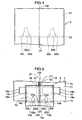
- FIG. 1 is a schematic diagram of an optical module according to a first embodiment of the invention.
- the optical module includes an emitter-side mounting substrate 1, a receiver-side mounting substrate 3 and an external waveguide substrate 2 which joins the two mounting substrates 1, 3 with optical coupling capability.
- upward and downward directions mean the upward and downward directions as illustrated in FIG. 1
- left and right directions mean directions perpendicular to the plane of paper of FIG. 1
- left and right sides of FIG. 1 are regarded as front and rear of the optical module, respectively.
- the emitter-side mounting substrate 1 has a generally rectangular shape in plan view which is elongate along a front-rear direction and has a thickness of approximately 200 ⁇ m to 2 mm. Overall dimensions of the mounting substrate 1 may differ depending on electrical and other components mounted thereon.
- the mounting substrate 1 has sufficient stiffness to prevent the influence of a stress due to thermal effects in mounting process and ambient conditions of use, for example.
- optical transmission efficiency between a light-emitting element and a light-detecting element is of substantial importance so that it is necessary to mount each optical element with high accuracy and avoid displacement thereof during operation as much as possible.
- a silicon substrate is used as the mounting substrate 1 in this embodiment.
- the mounting substrate 1 should preferably be made of a material having a coefficient of thermal expansion close to that of a light-emitting element 12a described below.
- the mounting substrate 1 may be made of a compound semiconductor like gallium arsenide (GaAs) which belongs to the same group as a below-described vertical cavity surface emitting laser (VCSEL) material.
- GaAs gallium arsenide
- VCSEL vertical cavity surface emitting laser
- Other alternatives include a ceramic substrate and a plastic substrate, the latter being usable depending on ambient conditions of use.
- the aforementioned light-emitting element 12a for converting an electric signal into a light signal and an integrated circuit (IC) board 4a on which an IC circuit for transmitting an electric signal is formed are mounted.
- the light-emitting element 12a used in this embodiment is a VCSEL which is a type of a semiconductor laser. While a light-emitting diode (LED) is an alternative to the semiconductor laser that can be employed as the light-emitting element 12a, the LED lacks directivity and, thus, the ratio of light coupled to a waveguide through a later-described 45-degree mirror surface is low. The LED which confers an advantage for its low cost may be employed on condition that optical efficiency is sufficiently high.
- LED light-emitting diode
- the light-emitting element 12a is mounted on the mounting substrate 1 by flip-chip bonding which provides, compared to die bonding and wire bonding, a greater degree of mounting accuracy as high as 1 ⁇ m or less with a capability to recognize an alignment mark printed on a chip.
- the IC board 4a is a driver IC located close to the light-emitting element 12a for driving the aforementioned VCSEL. Although not illustrated, the light-emitting element 12a and the IC board 4a are connected to a wiring pattern formed on the top surface 11 of the mounting substrate 1 via gold bumps. The IC board 4a and the light-emitting element 12a simultaneously mounted on the mounting substrate 1.
- underfill materials are filled between the light-emitting element 12a and the mounting substrate 1 and between the IC board 4a and the mounting substrate 1. It is required for the underfill material filled between the light-emitting element 12a and the mounting substrate 1 to have transparency to the wavelength of light emitted from the light-emitting element 12a as well as a certain degree of elasticity as the property of the VCSEL varies depending on a stress applied thereto. Silicone resin and epoxy resin are suitable examples of the underfill material used between the light-emitting element 12a and the mounting substrate 1. Epoxy resin is a suitable example of the underfill material used between the IC board 4a and the mounting substrate 1 from the viewpoint of mounting strength.
- the mounting substrate 1 has a waveguide 16 formed therein that is optically coupled to the light-emitting element 12a.
- This waveguide 16 extends rearward from the mirror portion 15 up to a rear end 10 of the mounting substrate 1 as shown in FIGS. 2B , 3A and 3B .
- the waveguide 16 includes a core 17 formed into a generally square cross-sectional shape to provide a high refractive index for propagating light and a cladding 18 having a lower refractive index than the core 17, the waveguide 16 extending in a waveguide groove 16a formed in the mounting substrate 1.
- a rear end surface of the core 17 in a longitudinal direction thereof is made generally flush with a rear end surface of the mounting substrate 1, the rear end surface of the core 17 constituting a first butt surface 17a which abuts a second butt surface 21a of a later-described core 21 of the external waveguide substrate 2.
- Dimensions of the core 17 and the cladding 18 of the waveguide 16 are determined based on the distance from the light-emitting element 12a to the waveguide 16, divergence angle of the light-emitting element 12a and size of a later-described light-detecting element 12b with first priority given to the optical efficiency.
- the VCSEL has an emitting beam diameter of 5-10 ⁇ m and a divergence angle of approximately 20 degrees and the photodiode has an detective diameter of approximately 60 ⁇ m, for example, so that it is preferable that the core 17 have a light path width of 40 ⁇ m and the cladding 18 have a thickness of 2-10 ⁇ m.
- the emitter-side mounting substrate 1 of the first embodiment has a pair of fitting recesses 13a, 13b formed therein to serve as first mating parts.
- the fitting recesses 13a, 13b are used for aligning and joining the mounting substrate 1 and the external waveguide substrate 2 so that axes of the core 17 of the waveguide 16 formed in the mounting substrate 1 and the later-described core 21 of an external waveguide formed in the external waveguide substrate 2 would not be offset from each other along the left-right direction (widthwise direction).
- the two fitting recesses 13a, 13b are formed on left and right sides of the core 17, respectively.
- the left-side fitting recess 13a is formed as if cut from the rear end 10 and the top surface 11 of the mounting substrate 1.
- An inner left side and an inner right side of the left-side fitting recess 13a form a left-side oblique wall 13c and a right-side oblique wall 13d, respectively.
- the left-side oblique wall 13c forms a surface oriented at a specific oblique angle relative to a longitudinal axis O1 of the core 17.
- the right-side oblique wall 13d also forms a surface oriented obliquely from the axis O1 but in an opposite direction. Therefore, as seen in plan view, the left-side fitting recess 13a is generally dovetail-shaped (tapered), gradually narrowing frontward from the rear end 10 of the mounting substrate 1.
- the right-side fitting recess 13b is similarly formed on a side opposite the left-side fitting recess 13a with respect to the axis O1 so that the left-side fitting recess 13a and the right-side fitting recess 13b are left-right symmetric.
- the right-side fitting recess 13b has a left-side oblique wall 13c and .a right-side oblique wall 13d formed like those of the left-side fitting recess 13a so that the right-side fitting recess 13b is generally dovetail-shaped (tapered) in plan view, gradually narrowing frontward from the rear end 10 of the mounting substrate 1 like the left-side fitting recess 13a.
- the left-side oblique wall 13c of the left-side fitting recess 13a and the right-side oblique wall 13d of the right-side fitting recess 13b are formed symmetrically on left and right sides of the axis O1, as are the right-side oblique wall 13d of the left-side fitting recess 13a and the left-side oblique wall 13c of the right-side fitting recess 13b.
- the top surface 11 of the mounting substrate 1 has an overlap area 14 overlapped by a later-described lap joint portion 5 of the external waveguide substrate 2 as well as a pair of adhesive filling recesses 19 into which adhesive is filled.
- the overlap area 14 in the top surface 11 of the mounting substrate 1 extends frontward from the rear end 10 by as much as the length of the lap joint portion 5.
- the adhesive filling recesses 19 are formed on the left and right sides of the axis O1 of the core 17 as depicted in FIGS. 3A and 3B .
- Each of the adhesive filling recesses 19 has an adhesive filling portion 19a and an adhesive inlet 19b through which the adhesive is filled into the adhesive filling portion 19a, the adhesive inlet 19b being connected to the adhesive filling portion 19a.
- Each adhesive filling portion 19a is an area where the lap joint portion 5 of the external waveguide substrate 2 is bonded, the adhesive filling portion 19a being formed in part of the overlap area 14 of the mounting substrate 1.
- Each adhesive inlet 19b is formed in part of a non-overlap area of the mounting substrate 1 where a top side of the mounting substrate 1 is not overlapped by the lap joint portion 5 of the external waveguide substrate 2.
- the adhesive filling recesses 19 are formed at the rear of the fitting recesses 13a, 13b at locations apart therefrom, each of the adhesive filling recesses 19 measuring approximately 50 ⁇ m to 300 ⁇ m deep from the top surface 11 of the mounting substrate 1 and approximately 100 ⁇ m to 1000 ⁇ m long (front to rear) and wide (left to right).
- the adhesive filling recesses 19 may have still larger depth depending on the thickness of the mounting substrate 1.
- the external waveguide substrate 2 has the earlier-mentioned external waveguide which is optically coupleable to both the core 17 of the waveguide 16 formed in the emitter-side mounting substrate 1 and a core 17 of a waveguide 16 formed in the receiver-side mounting substrate 3.
- the core 21 is formed all along the external waveguide substrate 2 so that an axis 02 of the core 21 generally aligns with a longitudinal axis of the external waveguide substrate 2.
- a front end surface of the core 21 of the external waveguide substrate 2 oriented frontward in a longitudinal direction of the core 21 constitutes the earlier-mentioned second butt surface 21a which abuts the first butt surface 17a of the mounting substrate 1 is made flush with a front end 20 of the external waveguide substrate 2 and exposed to the exterior.
- the external waveguide substrate 2 has at longitudinal ends thereof the earlier-mentioned lap joint portion 5 which is joined to the emitter-side mounting substrate 1 and another lap joint portion 5 which is joined to the receiver-side mounting substrate 3. Since these lap joint portions 5 are symmetrically shaped, the following discussion deals only with the lap joint portion 5 joined to the emitter-side mounting substrate 1 without describing the lap joint portion 5 joined to the receiver-side mounting substrate 3.
- the lap joint portion 5 is a platelike portion of the external waveguide substrate 2 which extends frontward beyond the front end 20 thereof, the lap joint portion 5 having the same width as a main portion of the external waveguide substrate 2 and a specific thickness.
- the lap joint portion 5 is formed as an integral part of the cladding 23 of the external waveguide substrate 2 using the same material as the cladding 23.
- a bottom side (top side as depicted in FIG. 2A ) of the lap joint portion 5 constitutes a contact surface 51 which goes into direct contact with the overlap area 14 of the emitter-side mounting substrate 1 when the lap joint portion 5 is placed to overlap the overlap area 14.
- the contact surface 51 is made generally flush with a top side of the core 21.
- left-side and right-side fitting tabs 22a, 22b serving as second mating parts which fit into the fitting recesses 13a, 13b formed in the emitter-side mounting substrate 1.
- the left-side fitting tab 22a fits into the left-side fitting recess 13a of the mounting substrate 1 while the right-side fitting tab 22b fits into the right-side fitting recess 13b of the mounting substrate 1.
- the left-side fitting tab 22a has a left-side contact wall 22c and a right-side contact wall 22d which go into contact with the left- and right-side oblique walls 13c, 13d of the left-side fitting recess 13a formed in the emitter-side mounting substrate 1, respectively.
- Distances of the left- and right-side contact walls 22c, 22d from the axis 02 of the core 21 of the external waveguide substrate 2 are made equal to distances of the left-and right-side oblique walls 13c, 13d of the left-side fitting recess 13a from the axis O1 of the core 17 of the mounting substrate 1 (refer to FIG. 3A ).
- the right-side fitting tab 22b also has a left-side contact wall 22c and a right-side contact wall 22d which go into contact with the left- and right-side oblique walls 13c, 13d of the right-side fitting recess 13b formed in the emitter-side mounting substrate 1, respectively.
- Distances of the left- and right-side contact walls 22c, 22d from the axis 02 of the core 21 of the external waveguide substrate 2 are made equal to distances of the left- and right-side oblique walls 13c, 13d of the right-side fitting recess 13b from the axis O1 of the core 17 of the mounting substrate 1.
- the first butt surface 17a of the core 17 of the emitter-side mounting substrate 1 is placed face to face with the second butt surface 21a of the core 21 of the external waveguide substrate 2. Since the cores 17, 21 of the mounting substrate 1 and the external waveguide substrate 2 are aligned along the left-right direction (widthwise direction) as a result of the above-described joining operation, the axis O1 of the mounting substrate 1 and the axis 02 of the external waveguide substrate 2 are aligned without offsetting laterally. Also as a result of this joining operation, the lap joint portion 5 of the external waveguide substrate 2 overlies the overlap area 14 of the mounting substrate 1 witch the contact surface 51 of the lap joint portion 5 held in face-to-face contact with the overlap area 14.
- the contact surface 51 of the external waveguide substrate 2 and the top side of the core 21 of the external waveguide substrate 2 are made flush with each other as are the overlap area 14 of the emitter-side mounting substrate 1 and the top side of the core 17 thereof, the axes O1, O2 of the respective cores 17, 21 are aligned to the same vertical position (in the thickness direction). Consequently, the core 17 of the emitter-side mounting substrate 1 and the core 21 of the external waveguide substrate 2 are optically coupled with substantially zero optical axis offsetting.
- the adhesive is filled into between the mounting substrate 1 and the external waveguide substrate 2 as described below.
- Vertical alignment of the mounting substrate 1 and the external waveguide substrate 2 in their stacking direction (thickness direction) is accomplished by using the contact surface 51 of the lap joint portion 5 of the external waveguide substrate 2 and the overlap area 14 of the mounting substrate 1 as reference planes.
- a retaining plate 70 (shown by alternate long and short dashed lines in FIG. 5 ) made of a glass plate, for instance, is placed on top of the lap joint portion 5 of the external waveguide substrate 2 in this embodiment.
- the retaining plate 70 thus disposed presses the aforementioned mating parts of the mounting substrate 1 and the external waveguide substrate 2 and the adhesive filling portions 19a of the mounting substrate 1 from above to prevent mutual position offset of the mounting substrate 1 and the external waveguide substrate 2 in the stacking direction thereof (or a lifting of the external waveguide substrate 2 from the mounting substrate 1) during adhesive filling operation.
- This arrangement of the embodiment serves to prevent vertical (thicknesswise) offset of the mounting substrate 1 and the external waveguide substrate 2, thus ensuring an increased positioning accuracy.
- the adhesive filling portions 19a of the adhesive filling recesses 19 formed in the mounting substrate 1 are covered by the lap joint portion 5 of the external waveguide substrate 2 from above.
- the adhesive is filled into the adhesive filling recesses 19 through the adhesive inlets 19b thereof in this condition.
- the adhesive penetrates into the adhesive filling portions 19a through the adhesive inlets 19b by capillary action so that the adhesive filling portions 19a of the mounting substrate 1 are bonded to an area of the lap joint portion 5 of the external waveguide substrate 2 facing the adhesive filling recesses 19 by the adhesive.
- the adhesive does not penetrate in between the fitting tabs 22a, 22b of the lap joint portion 5 of the external waveguide substrate. 2 and the fitting recesses 13a, 13b formed in the mounting substrate 1.
- the emitter-side mounting substrate 1 and the external waveguide substrate 2 are held in alignment even after the aforementioned adhesive filling process.
- This makes it possible to prevent the cores 17, 21 of the emitter-side mounting substrate 1 and the external waveguide substrate 2 from offsetting from each other in the left-right direction due to the presence of the adhesive.
- no adhesive exists between the external waveguide substrate 2 and an area of the top surface of the mounting substrate 1 excluding the adhesive filling recesses 19 formed therein, it is possible to prevent vertical offsetting of the emitter-side mounting substrate 1 and the external waveguide substrate 2.
- the above-described arrangement of the present embodiment ensures that the adhesive used for bonding the mounting substrate 1 (3) to the external waveguide substrate 2 can be applied without risk of adhering to the light-emitting element 12a (light-detecting element 12b) and the IC board 4a (4b).
- the adhesive used in this embodiment is a thermosetting epoxy adhesive
- the adhesive is not limited thereto.
- the optical module of the first embodiment is an optoelectric transducer
- the invention is applicable to optical coupling of waveguides formed in a pair of substrates.
- the above-described configuration of the first embodiment is also applicable to a passive device not having a light-emitting or light-detecting element like an optical splitter and a waveguide film.
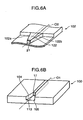
- An optical module according to a second embodiment of the invention is described with reference to FIGS. 6A and 6B .
- An emitter-side mounting substrate 100 of the optical module of the second embodiment has a single fitting recess 113.
- the fitting recess 113 has a left-side oblique wall 104 and a right-side oblique wall 105 which are formed such that the fitting recess 113 is generally dovetail-shaped (tapered) in plan view, gradually narrowing frontward as depicted in FIG. 6B .
- the left-side oblique wall 104 is located on a left side of an axis O1 of a core 17 of a waveguide 16 and the right-side oblique wall 105 is located on a right side of the axis O1 of the core 17 of the waveguide 16.
- the left- and right-side oblique walls 104, 105 are formed symmetrically on the left and right sides of the axis O1 of the core 17 of the waveguide 16, respectively.
- an external waveguide substrate 102 of the second embodiment has a single fitting tab 122 shaped to fit into the fitting recess 113 formed in the mounting substrate 100, the fitting tab 122 having a left-side contact wall 122a and a right-side contact wall 122b which go into contact with the left- and right-side oblique walls 104, 105 of the fitting recess 113, respectively. Also, the left- and right-side contact walls 122a, 122b are formed symmetrically on left and right sides of an axis 02 of a core 21 of the external waveguide substrate 102, respectively, in terms of both shape and location.
- the second embodiment it is possible to maintain the left- and right-side contact walls 122a, 122b in the same bilaterally symmetrical shape and location with respect to the axis 02 of the core 21 even when the external waveguide substrate 102 expands or shrinks due to a thermal effect, for instance.
- This makes it possible to align the core 17 of the mounting substrate 100 and the core 21 of the external waveguide substrate 102 with increased accuracy by fitting the fitting tab 122 of the external waveguide substrate 102 into the fitting recess 113 of the mounting substrate 100.
- An emitter-side mounting substrate 301 of the optical module of this embodiment has a plurality of adhesive filling recesses 319 which are formed close to left and right rear portions of each of fitting recesses 313a, 313b in such a manner that the adhesive filling recesses 319 connect to the respective fitting recesses 313a, 313b.
- a lap joint portion 305 of an external waveguide substrate 2 has a pair of fitting tabs 322a, 322b, each of the fitting tabs 322a, 322b having a left-side contact wall 322c and a right-side contact wall 322d. Basal parts of the left- and right-side contact walls 322c, 322d serve as bonding areas 320.
- the fitting tabs 322a, 322b of the lap joint portion 305 of the external waveguide substrate 2 are fitted into the fitting recesses 313a, 313b of the mounting substrate 301, respectively, whereby the adhesive filling recesses 319 are bonded to the respective bonding areas 320 of the lap joint portion 305.
- the left- and right-side contact walls 322c, 322d of the fitting tabs 322a, 322b of the lap joint portion 305 go into contact with left- and right-side oblique walls 313c, 313d of the fitting recesses 313a, 313b, respectively.
- FIGS. 8A and 8B show an example of an alternative arrangement in which, by analogy with the adhesive filling recesses 19 of the first embodiment (see FIGS. 3A and 3B ), a pair of adhesive filling recesses 319c each having an adhesive filling portion 319a and an adhesive inlet 319b are formed in atop surface of the mounting substrate 301, the adhesive filling portions 319a connecting to forward ends (rear ends) of the respective fitting recesses 313a, 313b.
- the lap joint portion 305 of the external waveguide substrate 2 is configured such that fitting tabs 322a, 322b formed on the lap joint portion 305 each have bonding areas 320a close to front ends of left- and right-side contact walls 322c, 322d.
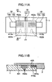
- the optical module of this embodiment is configured such that a pair of adhesive bonding projections 452 is formed on a lap joint portion 405 of an external waveguide substrate 2, the adhesive bonding projections 452 protruding downward from a contact surface 451 (bottom side) of the lap joint portion 405 toward respective adhesive filling recesses 19 formed in a top surface of an emitter-side mounting substrate 1.
- the adhesive bonding projections 452 are fitted into adhesive filling portions 19a of the respective adhesive filling recesses 19 in the top surface of the mounting substrate 1 and bonded thereto by the adhesive filled into the adhesive filling portions 19a.
- the above-described configuration of the third embodiment is advantageous in that it is possible to securely join the mounting substrate 1 and the external waveguide substrate 2 to each other.
- FIGS. 11A and 11B is a variation of the thrid embodiment in which a plurality of adhesive bonding projections 452a are formed on each side (left and right) of the core 21 of the external waveguide substrate 2.
- An arrangement including a plurality of adhesive bonding projections 452a is preferable because this kind of arrangement can provide a yet larger adhesive bonding area and, thus, more securely join the mounting substrate 1 and the external waveguide substrate 2 to each other.
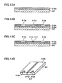
- the same cladding material as used for forming the underlying cladding layer 518a was applied to form an outer cladding layer 518b on top of the underlying cladding layer 518a, and the core groove 517a and the fitting recesses 513a, 513b were formed in the outer cladding layer 518b by processing the same to create a prescribed pattern therein as shown in FIG. 12B .
- the core material used was an epoxy material similar to the cladding material used for forming the underlying cladding layer 518a, the core material having a refractive index higher than the cladding material by as much as 0.02 to 0.10.
- the core material was cured by irradiating the same with ultraviolet light for 30 seconds to 3 minutes at an intensity of 30 mW/cm 2 .
- a one-piece forming procedure for forming the fitting tabs 522a, 522b and the core 521 in the external waveguide substrate 502 is discussed referring to an experiment conducted by the inventors.
- a cladding material was applied to one side of the external waveguide substrate 502 to form an underlying cladding layer 523a, the cladding material being the same as used for forming the mounting substrate 501.
- the external waveguide substrate 502 of this embodiment interconnects multiple devices and transmits signals therebetween so that the external waveguide substrate 502 is required to provide ease of handling and flexibility to durability of ambient conditions.
- a film material was used as the external waveguide substrate 502 of this embodiment. Specifically, a polyimide film used in a flexible board or, from a viewpoint of ease of later handling, a transparent film made of polyethylene terephthalate (PET) was used as a base material of the external waveguide substrate 502.
- PET polyethylene terephthalate
- a photosetting epoxy material is used as the cladding material for forming the underlying cladding layer 523a.
- the external waveguide substrate 502 itself may be formed by the same cladding material, in which case the external waveguide substrate 502 is configured with the underlying cladding layer 523a alone.
- a core material was applied by spin coating on top of the underlying cladding layer 523a and a layer of the spin-coated core material was exposed and developed to form the fitting tabs 522a, 522b and the core 521.
- the core material used is the same as used for forming the mounting substrate 501.
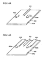
- fitting tabs 522a, 522b of the external waveguide substrate 502 may be simply dovetail-shaped (tapered) in plan view as depicted in FIG. 14A
- the fitting tabs 522a, 522b may be formed integrally with respective prismatic-bar-shaped projections 530 extending generally parallel to the core 521 along a longitudinal direction thereof as depicted in FIG. 14B , the prismatic-bar-shaped projections 530 being made of the same material as used for forming the core 521.
- the provision of the aforementioned prismatic-bar-shaped projections 530 serves to prevent mutual position offset of the fitting tabs 522a, 522b and the core 521. This is because the external waveguide substrate 502 will expand or shrink isotropically even when shrinkage on curing of resin or thermal expansion or shrinkage occurs.
- the photosetting epoxy material was used in the mounting substrate 501 and the external waveguide substrate 502 of the fifth embodiment as discussed above, the invention is not limited thereto.
- the optical module of this embodiment comprises an emitter-side mounting substrate 601 having a pair of fitting recesses 613a, 613b formed in specified areas of a top surface thereof. These areas of the top surface of the mounting substrate 601 where the fitting recesses 613a, 613b are formed are made of a material different from a base material of the mounting substrate 601. A procedure for producing such a configuration is described in detail below.
- two fitting recess forming cavities 630, 630 are formed in left and right rear portions of the top surface of a silicon substrate constituting the mounting substrate 601, wherein the two fitting recess forming cavities 630 are hollows having larger surface areas than the fitting recesses 613a, 613b and a greater depth than an intended depth thereof below the top surface of the mounting substrate 601.
- a waveguide forming groove 616a having a rectangular cross section is formed in the top surface of the mounting substrate 601, the waveguide forming groove 616a running generally along a longitudinal center line of the mounting substrate 601.
- the aforementioned fitting recess forming cavities 630 and waveguide forming groove 616a can be formed by an etching process, for example.
- the mounting substrate 601 of this embodiment has a thickness between 300 ⁇ m and 500 ⁇ m, and each of the fitting recess forming cavities 630 is approximately 40 ⁇ m to 100 ⁇ m long and wide as measured along a longitudinal direction and a left-right direction of the mounting substrate 601, respectively.
- the fitting recess forming cavities 630 and the waveguide forming groove 616a are filled with a cladding material and, then, the aforementioned fitting recesses 613a, 613b and a cladding 618 having a rectangular-shaped cross section are formed in the top surface of the mounting substrate 601 by press-forming the cladding material filled therein by using a die having a pair of fitting recess forming shapes and a cladding forming shape.
- a core 617 of the mounting substrate 601 is formed by filling a core material into a core groove 617a formed within the cladding 618.
- the material filled into the fitting recess forming cavities 630 for forming the fitting recesses 613a, 613b is not limited to the aforementioned cladding material but may be selected as appropriate.
- the fitting recesses 613a, 613b of this embodiment has approximately the same dimensions as the fitting recesses 13a, 13b of the earlier-described first embodiment.
- fitting recesses 613a, 613b are formed in the cladding material filled into the fitting recess forming cavities 630 of the mounting substrate 601, it is possible to form the fitting recesses 613a, 613b by hollowing the cladding material downward from the top surface of the mounting substrate 601. If the fitting recesses 613a, 613b are to be formed in a cladding layer deposited on top of the mounting substrate 601 by using an embossing die as in the foregoing fourth embodiment, for instance, it is necessary to form the cladding layer on the top surface of the mounting substrate 601 so that it would be difficult to reduce the overall thickness of the finished mounting substrate 601.
- the overall thickness of the finished mounting substrate 601 is defined by the thickness of the silicon substrate used for constituting the mounting substrate 601 alone. This makes it easier to achieve a reduction in the overall size and thickness of the finished mounting substrate 601. While a top surface of each fitting recess forming cavity 630 is made generally flush with the top surface of the mounting substrate 601 in the above-described fifth embodiment, this configuration may be modified such that the former is higher or lower than the latter.
- the optical module of this embodiment comprises an emitter-side mounting substrate 701 having a core 717 formed therein and an external waveguide substrate 702.
- a first butt surface 717a of a core 717 formed in the mounting substrate 701 is a slant surface which is inclined such that the distance between the first butt surface 717a and a core 721 formed in the external waveguide substrate 702 gradually decreases upward toward a lap joint portion 705 of the mounting substrate 701.
- a result of this configuration is that even when the core 717 of the emitter-side mounting substrate 701 is located at a position lower than the core 721 of the external waveguide substrate 702, light propagating through the core 717 of the mounting substrate 701 toward the external waveguide substrate 702 is refracted obliquely upward at the first butt surface 717a and enters the core 721 of the external waveguide substrate 702 through a second butt surface 721a thereof.
- This feature of the embodiment helps reduce optical coupling loss.
- a second butt surface 721a of the core 721 formed in the external waveguide substrate 702 that abuts a first butt surface 717a of a core 717 formed in a receiver-side mounting substrate 703 is also a slant surface which is inclined such that the distance between the second butt surface 721a of the core 721 formed in the external waveguide substrate 702 and the core 717 formed in the receiver-side mounting substrate 703 gradually increases upward toward a lap joint portion 705 of the mounting substrate 703.
- the adhesive layer 700 is also formed between the receiver-side mounting substrate 703 and the lap joint portion 705.
- a result of this configuration is that even when the core 717 of the receiver-side mounting substrate 703 is located at a position lower than the core 721 of the external waveguide substrate 702, light propagating through the core 721 of the external waveguide substrate 702 toward the mounting substrate 703 is refracted obliquely downward at the second butt surface 721a and enters the core 717 of the receiver-side mounting substrate 703.
- This feature of the embodiment also helps reduce optical coupling loss.
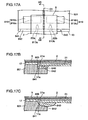
- the optical module of this embodiment comprises an emitter-side mounting substrate 801 of which rear end 10 is shaped to form a socket 840 into which a front end of an external waveguide substrate 2 is fitted and attached.
- the aforementioned socket 840 is formed by cutting an upper part of the rear end 10 of the emitter-side mounting substrate 801 all along the width thereof, the socket 840 having a side surface (a vertical surface) 841 which is generally perpendicular to an axis 01 of a core 17 formed in the emitter-side mounting substrate 801 and a bottom surface 842 formed generally at right angles to the side surface 841.
- a first butt surface 17a of the core 17 is generally flush with the side surface 841 of the socket 840.
- the emitter-side mounting substrate 801 of this embodiment is provided with a pair of adhesive filling recesses 819 having essentially the same configuration as the adhesive filling recesses 19 of the emitter-side mounting substrate 1 of the earlier-described first embodiment.
- the mounting substrate 1 and the external waveguide substrate 2 it is possible to bond the mounting substrate 1 and the external waveguide substrate 2 to each other not only at the adhesive filling recesses 819 but also at the socket 840, thus producing an increased adhesive bonding area and greater bond strength.
- This configuration also ensures that a second butt surface 21a of a core 21 of the external waveguide substrate 2 would not be separately from the first butt surface 17a of the core 17 of emitter-side mounting substrate 1 when the external waveguide substrate 2 is warped.
- the socket 840 should be 50 ⁇ m to 400 ⁇ m deep.
- a method of forming the socket 840 on the mounting substrate 801 is not particularly limited. For example, a half cutting dicing technique or a dry etching technique, such as reactive ion etching (RIE) process, may be used for forming the socket 840.
- the socket 840 is not limited to the shape shown in FIG. 17B but may be shaped to have a curved surface along the aforementioned side surface 841 and bottom surface 842 as depicted in FIG. 17C , for example.
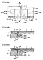
- the socket 940 formed in the emitter-side mounting substrate 901 of the ninth embodiment has basically the same configuration as the socket 840 of the above-described configuration of the seventh embodiment.
- the aforementioned groove 943 is formed in a bottom surface 942 of the socket 940.
- the groove 943 is formed to a specific depth and width along a side surface (a vertical surface) 941 of the socket 940.
- the adhesive applied to the socket 940 can easily enter the groove 943 by capillary action. Additionally, the adhesive which has once entered the groove 943 would not easily go out of the groove 943 due to anchoring effect and this serves to produce an increased bond strength.
- the width of the groove 943 is not particularly limited either, so that the groove 943 may be formed all along the width of the socket 940 (mounting substrate 901) or generally along the width of the external waveguide substrate 2, for example.
- the aforementioned groove 943 is not limited to a particular shape.
- the groove 943 need not necessarily have a rectangular cross section as shown in FIG. 18B but may be modified to have a different cross-sectional shape as appropriate, such as a semicircular cross section as shown in FIG. 18C , for example.
- the groove 943 may be formed by the half cutting dicing technique or dry etching technique, such as the RIE process, for instance.
- the optical module also comprises an external waveguide substrate 1002 which is configured such that a second butt surface 1021a of a core 1021 formed in the external waveguide substrate 1002 is formed at a location determined in relation to fitting tabs 1022a, 1022b formed on the external waveguide substrate 1002.
- the core 1021 is configured to project frontward so that the second butt surface 1021a is located to the front of a front end 1020 of the external waveguide substrate 1002 as depicted in FIG. 19B .
- the ninth embodiment it is possible to always locate the second butt surface 1021a of the core 1021 of the external waveguide substrate 1002 at a fixed position relative to the first butt surface 1017a of the core 1017 of the emitter-side mounting substrate 1001 regardless of the location of the rear end 1010 of the emitter-side mounting substrate 1001. This serves to provide an improved optical coupling efficiency.
- the distance between the first butt surface 1017a and the rear end 1010 is approximately 20 ⁇ m to 100 ⁇ m if only the manufacturing error is taken into consideration, the distance may be of 100 ⁇ m to 3 mm according to the present embodiment of the invention, because the configuration of this embodiment allows for a high degree of freedom in design with respect to an overall arrangement pattern of the optical module.
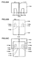
- the optical module of this example comprises an emitter-side mounting substrate 1101 which is provided with one fitting tab 1113 as shown in FIG. 20A and an external waveguide substrate 1102 of which lap joint portion 1105 is provided with one fitting recess 1122 as shown in FIG. 20B ,.
- the emitter-side mounting substrate 1101 of the second example has a left-side recess 1141 and a right-side recess 1142 which are provided on left and right sides of a core 1117 formed in the mounting substrate 1101, respectively.
- a right-hand inner surface of the left-side recess 1141 forms a surface oriented at a specific oblique angle relative to a longitudinal axis 01 of the core 1117.
- This obliquely oriented surface constitutes a first contact surface 1113a which goes into contact with a below-described first oblique surface 1122a of the fitting recess 1122 of the lap joint portion 1105.
- a left-hand inner surface of the right-side recess 1142 constitutes a second contact surface 1113b which goes into contact with a below-described second oblique surface 1122b of the fitting recess 1122 of the lap joint portion 1105.
- the first and second contact surfaces 1113a, 1113b are located symmetrically on left and right sides the axis 01.
- the first and second contact surfaces 1113a, 1113b thus structured together form the aforementioned fitting tab 1113 which is generally dovetail-shaped in plan view, gradually widening frontward (upward in FIG. 20A ).
- the lap joint portion 1105 of the external waveguide substrate 1102 of the seconde example has a left-side tab 1143 and a right-side tab 1144 which are provided on left and right sides of a core 1121 formed in the external waveguide substrate 1102, respectively.
- the left-side tab 1143 of the external waveguide substrate 1102 has a proper size and shape to fit into the left-side recess 1141 of the mounting substrate 1101.
- a right-hand side surface of the left-side tab 1143 is located relative to an axis 02 of the core 1121 of the external waveguide substrate 1102 in the same way as the first contact surface 1113a of the mounting substrate 1101 is located relative to the axis 01 of the core 1117 of the mounting substrate 1101.
- the right-hand side surface of the left-side tab 1143 thus structured constitutes the aforementioned first oblique surface 1122a.
- the right-side tab 1144 of the external waveguide substrate 1102 has a proper size and shape to fit into the right-side recess 1142 of the mounting substrate 1101.
- a left-hand side surface of the right-side tab 1144 is located relative to an axis 02 of the core 1121 of the external waveguide substrate 1102 in the same way as the second contact surface 1113b of the mounting substrate 1101 is located relative to the axis 01 of the core 1117 of the mounting substrate 1101.
- the left-hand side surface of the right-side tab 1144 thus structured constitutes the aforementioned second oblique surface 1122b.
- the first and second oblique surfaces 1122a, 1122b together form the aforementioned fitting recess 1122 which is generally dovetail-shaped in plan view, gradually widening frontward (upward in FIG. 20B ).
- the external waveguide substrate 1102 is relatively moved toward the mounting substrate 1101 from the rear side thereof so that the left- and right-side tabs 1143, 1144 on the lap joint portion 1105 fit into the left- and right-side recesses 1141, 1142 of the mounting substrate 1101, respectively.
- the first and second oblique surfaces 1122a, 1122b of the lap joint portion 1105 go into contact with the first and second contact surfaces 1113a, 1113b of the emitter-side mounting substrate 1101 as depicted in FIG. 20C , as a result, the fitting tab 1113 of the emitter-side mounting substrate 1101 is fitted into the fitting recess 1122 formed in the lap joint portion 1105 of the external waveguide substrate 1102.
- the optical module of this embodiment comprises an emitter-side mounting substrate 1201 and an external waveguide substrate 1202 which are joined together at first and second mating parts thereof with adhesive.
- the optical module of the tenth embodiment is described in detail below.
- the top side of the mounting substrate 1201 includes the overlap area 1214 overlapped by a later-described lap joint portion 1205 of the external waveguide substrate 1202 and a non-overlap area 1215 where the top side of the mounting substrate 1201 is not overlapped by the lap joint portion 1205 as shown in FIG. 22 .
- the fitting recesses 1213a, 1213b are formed in the overlap area 1214 of the mounting substrate 1201 to a specific depth below the overlap area 1214.
- adhesive inlets 1219b connected to the respective adhesive filling portions 1219a are formed in the non-overlap area 1215. Adhesive is filled into the adhesive filling portions 1219a through these adhesive inlets 1219b.
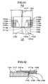
- a core 1217 formed in the mounting substrate 1201 is covered with a cladding in actuality (see FIG. 23 ), the cladding is not shown in FIG. 21 for the sake of simplicity as is the case with FIGS. 22 , 24-33 , 35 , 37-42 .
- the fitting recesses 1213a, 1213b of the mounting substrate 1201 of the tenth embodiment thus configured are bonded to fitting tabs 1222a, 1222b, respectively, by the adhesive. Described below is a procedure for joining the mounting substrate 1201 and the external waveguide substrate 1202 to each other by adhesive bonding.
- the mounting substrate 1201 and the external waveguide substrate 1202 are placed such that oblique outside walls of the fitting tabs 1222a, 1222b of the external waveguide substrate 1202 go into contact with oblique inside walls of the fitting recesses 1213a, 1213b of the mounting substrate 1201, respectively, as shown in FIGS. 22 and 23 .
- the fitting tabs 1222a, 1222b of the external waveguide substrate 1202 fit into the respective fitting recesses 1213a, 1213b of the mounting substrate 1201 as a consequence.
- the adhesive (not shown) is filled into the adhesive filling portions 1219a through the respective adhesive inlets 1219b in this condition.
- a prescribed amount of adhesive having a viscosity of about 0.05 Pa ⁇ s is applied by dropping the same through the adhesive inlets 1219b by use of a dispenser.
- the prescribed amount of adhesive is filled into the significantly small-sized adhesive filling portions 1219a of the mounting substrate 1201 in this way. It is to be noted, however, that the invention is not limited to the aforementioned adhesive filling method, but any other appropriate method may be used for applying the adhesive.
- the dispensed adhesive fills into the adhesive filling portions 1219a and penetrates therefrom into gaps between the fitting recesses 1213a, 1213b and the fitting tabs 1222a, 1222b by capillary action so that the fitting tabs 1222a, 1222b of the external waveguide substrate 1202 are bonded to the respective fitting recesses 1213a, 1213b of the mounting substrate 1201.
- the tenth embodiment it is possible to accurately align the core 1217 of the mounting substrate 1201 and the core 1221 of the external waveguide substrate 1202 with each other and join the mounting substrate 1201 and the external waveguide substrate 1202 under conditions where the cores 1217, 1221 are so aligned. Furthermore, as the emitter-side mounting substrate 1201 and the external waveguide substrate 1202 are held secured bonded to each other upon completion of the bonding procedure, it is possible to prevent mutual position offset of the mounting substrate 1201 and the external waveguide substrate 1202 in a reliable fashion.
- the invention is not limited to this procedure but may be modified to use a different adhesive dispensing method.
- the mounting substrate 1201 and the external waveguide substrate 1202 may be joined together after applying the adhesive to the inside walls of the fitting recesses 1213a, 1213b or the outside walls of the fitting tabs 1222a, 1222b, or to the walls of both the mounting substrate 1201 and the external waveguide substrate 1202.
- the adhesive filling portions 1219a may be either connected or unconnected to the respective fitting recesses 1213a, 1213b.
- adhesive to be dispensed after mating the mounting substrate 1201 and the external waveguide substrate 1202 is not limited to any particular type, adhesive with a viscosity of 0.005 to 10 Pa ⁇ s is preferable, because such adhesive can easily penetrate into gaps of approximately a few ⁇ m formed between the fitting recesses 1213a, 1213b and the fitting tabs 1222a, 1222b.
- the optical module of this embodiment comprises an emitter-side mounting substrate 1301 and an external waveguide substrate 1302. What is characteristic of this embodiment is that there are formed adhesive guiding grooves 1360 in an overlap area 1314 of the mounting substrate 1301.
- the adhesive guiding grooves 1360 are configured to allow the adhesive to smoothly flow into a gap created between a first butt surface 1317a of a core 1317 of the mounting substrate 1301 and a second butt surface 1321a of a core 1321 of the external waveguide substrate 1302 when the two cores 1317, 1321 are abutted against each other.
- each adhesive guiding groove 1360 between the first and second ends 1360a, 1360b thereof is located between the fitting recess 1313a (1313b) and the core 1317 as illustrated.
- the optical module of the eleventh embodiment has otherwise the same configuration as the above-described tenth embodiment.
- the adhesive is applied through adhesive inlets 1319b under conditions where the mounting substrate 1301 and the external waveguide substrate 1302 are mated with each other with fitting tabs 1322a, 1322b on the external waveguide substrate 1302 fitted into the respective fitting recesses 1313a, 1313b of the mounting substrate 1301 as in the above-described tenth embodiment.
- the adhesive filled into the adhesive filling portions 1319a penetrates therefrom into gaps created between the fitting recesses 1313a, 1313b and the respective fitting tabs 1322a, 1322b and also flows from the adhesive filling portions 1319a up to the rear end 1310 of the mounting substrate 1301 by capillary action.
- the adhesive (designated by the numeral 1300 in FIG. 26 ) which has flowed up to the rear end 1310 further flows into a gap created between the rear end 1310 of the mounting substrate 1301 and a facing front end 1320 of the external waveguide substrate 1302 as illustrated.
- the adhesive 1300 flows also into the gap created between the first butt surface 1317a of the core 1317 of the mounting substrate 1301 and the second butt surface 1321a of the core 1321 of the external waveguide substrate 1302.
- the gap between the rear end 1310 of the mounting substrate 1301 and the front end 1320 of the external waveguide substrate 1302 and the gap between the first and second butt surfaces 1317a, 1321a are represented in relatively larger dimensions compared to the mounting substrate 1301 and associated elements in FIG. 26 . In actuality, these gaps are much narrower than illustrated compared to the mounting substrate 1301 and the associated elements.
- the adhesive guiding grooves 1360 connect to the respective adhesive filling portions 1319a in the above-described configuration of the embodiment, this configuration may be varied such that the adhesive guiding grooves 1360 are formed separately from the adhesive filling portions 1319a, for example.
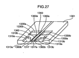
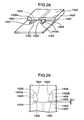
- FIG. 27 Shown in FIG. 27 is an example of such a variation of the eleventh embodiment. Specifically, there may be formed second adhesive filling portions 1330a at the rear of the adhesive filling portions 1319a, the second adhesive filling portions 1330a connecting to first ends 1360a of adhesive guiding grooves 1360 as shown in the example of FIG. 27 . In addition, there may also be formed second adhesive inlets 1330b connecting to the respective second adhesive filling portions 1330a.
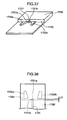
- the optical module comprising an emitter-side mounting substrate 1401 and an external waveguide substrate 1402 is configured such that, as shown in FIG. 30 , adhesive filling portions 1419a of the mounting substrate 1401 adjoin front, rear and outwardly oriented side walls of fitting tabs 1422a, 1422b of the external waveguide substrate 1402 fitted into fitting recesses 1413a, 1413b of the mounting substrate 1401.
- the adhesive filling portions 1419a of the mounting substrate 1401 are formed to adjoin the front, rear and outwardly oriented side walls of the respective fitting tabs 1422a, 1422b.
- the fitting tabs 1422a, 1422b of the external waveguide substrate 1402 are located in front of a front end 1420 of the external waveguide substrate 1402 at a specific distance L1 therefrom. With this arrangement, there are formed gaps 1425 between the fitting tabs 1422a, 1422b and the front end 1420 of the external waveguide substrate 1402.
- each of the fitting tabs 1422a, 1422b of the external waveguide substrate 1402 has outside walls which include the front and rear walls, an inwardly oriented side wall forming an oblique angle to the front and rear walls, and the outwardly oriented side wall forming generally a right angle to the front and rear walls.
- This configuration of the present embodiment makes it possible to securely bond the fitting tabs 1422a, 1422b of the external waveguide substrate 1402 to the fitting recesses 1413a, 1413b of the mounting substrate 1401, thereby making mutual position offset of the mounting substrate 1401 and the external waveguide substrate 1402 unlikely to occur regardless of ambient temperature changes or an external stress applied to the optical module.
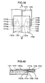
- the adhesive filling portions 1419a may be formed at positions slightly offset frontward so that the rear ends of the adhesive filling portions 1419a are located in front of the rear end 1410 of the mounting substrate 1401 at a distance L2 therefrom as depicted in FIG. 31 .
- This variation of the twelfth embodiment is advantageous in that this alternative arrangement serves to prevent or reduce the risk of outflow of the adhesive out of the rear end 1410 of the mounting substrate 1401 once filled into the adhesive filling portions 1419a.
- the optical module of this embodiment comprises an emitter-side mounting substrate 1501 and an external waveguide substrate 1502 of which lap joint portion 1505 has a plurality of deaeration holes 1580.
- the lap joint portion 1505 of the external waveguide substrate 1502 has facing surface areas 1581 which are positioned face to face with adhesive filling portions 1519a of the mounting substrate 1501 when the mounting substrate 1501 and the external waveguide substrate 1502 are mated in a manner that the lap joint portion 1505 of the latter overlies an overlap area 1514 of the former.
- the aforementioned deaeration holes 1580 are formed in the lap joint portion 1505 of the external waveguide substrate 1502. These deaeration holes 1580 serve to remove air bubbles which could form in adhesive filled into the adhesive filling portions 1519a of the mounting substrate 1501.
- optical module of the thirteenth embodiment it is possible to remove air bubbles from inside the adhesive filling portions 1519a of the mounting substrate 1501 through the deaeration holes 1580 even if the air bubbles form when the adhesive is filled into the adhesive filling portions 1519a of the mounting substrate 1501 through adhesive inlets 1519b formed therein.
- This arrangement of the present embodiment serves to prevent a reduction in bonding area between the facing areas 1581 of the lap joint portion 1505 of the external waveguide substrate 1502 and the adhesive filled into the adhesive filling portions 1519a of the mounting substrate 1501 as well as a reduction in bond strength.
- the optical module of this embodiment comprises an emitter-side mounting substrate 1601 having a core 1617 formed in a top surface thereof, wherein an adhesive guiding groove 1682 is formed in a top side of the core 1617.
- the core 1617 of the mounting substrate 1601 of the sixteenth embodiment is located at a specific depth below an overlap area 1614 of the top surface of the mounting substrate 1601.
- the aforementioned adhesive guiding groove 1682 is formed as if cut into the mounting substrate 1601 below the top surface thereof in the overlap area 1614 over a specified length along a longitudinal direction of the core 1617.
- the adhesive guiding groove 1682 connects to adhesive filling portions 1619a of the mounting substrate 1601 through respective narrow grooves 1682a formed therein.
- the adhesive guiding groove 1682 is formed over the aforementioned specified length from a first butt surface 1617a of the core 1617 along the longitudinal direction thereof, the adhesive guiding groove 1682 having a larger width than the core 1617.
- Adhesive filled into the adhesive guiding groove 1682 of this embodiment has the same refractive index as a material used for forming a cladding 1618 (shown in FIG. 36 ) which covers the left and right sides and bottom of the core 1617 of the mounting substrate 1601.
- the optical module of the fourteenth embodiment has otherwise the same configuration as the above-described tenth embodiment.
- the adhesive guiding groove 1682 connects to the adhesive filling portions 1619a through the narrow grooves 1682a in this embodiment, it is only necessary to dispense the adhesive into the adhesive inlets 1619b, thereby permitting a simplified manufacturing process.
- the adhesive can function as part of a cladding layer. Since an air gap would hardly be created between the core 1617 and this part the cladding layer formed by the adhesive, the adhesive covering the top side of the core 1617 can perform substantially the same function as the cladding 1618 covering the left and right sides and bottom of the core 1617.
- the adhesive guiding groove 1682 of the fourteenth embodiment is formed over the specified length from the first butt surface 1617a of the core 1617 along the longitudinal direction thereof, the invention is not limited thereto but this arrangement, of the embodiment may be modified as appropriate.
- the adhesive guiding groove 1682 may be formed over a specific length frontward from a position at a particular distance to the front of the first butt surface 1617a of the core 1617 along the longitudinal direction.
- the width of the adhesive guiding groove 1682 is not particularly limited, so that the adhesive guiding groove 1682 may be made narrower than the core 1617. In a case where the adhesive is used to constitute part the cladding layer, however, it is preferable that the width of the adhesive guiding groove 1682 be made equal to or larger than the width of the core 1617.
- the adhesive guiding groove 1682 may be formed to encompass an entire area from the left-side adhesive filling portion 1619a to the right-side adhesive filling portion 1619a, for example.
- a lap joint portion 1605 of the external waveguide substrate 1602 placed on the overlap area 1614 may partly settle into the adhesive guiding groove 1682 and warp. It is therefore preferable to form the adhesive guiding groove 1682 to overlap only part of the left- and right-side adhesive filling portions 1619a.
- the optical module of this embodiment is configured such that a front end 1720 of an external waveguide substrate 1702 is positioned face to face with a rear end 1710 of a mounting substrate 1701 when the mounting substrate 1701 and the external waveguide substrate 1702 are mated with each other with fitting tabs 1722a, 1722b of the latter fitted into fitting recesses 1713a, 1713b of the former, respectively.
- the rear end 1710 of the mounting substrate 1701 and the front end 1720 of the external waveguide substrate 1702 constitute end surfaces which are positioned face to face with each other.
- a front end portion 1721b of a core 1721 of the external waveguide substrate 1702 sticks out frontward to the exterior of the external waveguide substrate 1702 by a specific length L3.
- a forward end surface of this end portion 1721b of the core 1721 constitutes a second butt surface 1721a which is positioned face to face with a first butt surface 1717a of a core 1717 of the mounting substrate 1701.
- the optical module of the fifteenth embodiment has otherwise the same configuration as the earlier-described tenth embodiment.
- the fitting tabs 1722a, 1722b of the external waveguide substrate 1702 are fitted into the fitting recesses 1713a, 1713b of the mounting substrate 1701 as shown in FIG. 39 .
- the first butt surface 1717a and the second butt surface 1721a of the two cores 1717, 1721 are abutted against each other and the rear end 1710 of the mounting substrate 1701 and the front end 1720 of the external waveguide substrate 1702 are positioned face to face.
- the groovelike gap 1785 there is formed a groovelike gap 1785 between the two facing ends 1710, 1720 of the mounting substrate 1701 and the external waveguide substrate 1702, the groovelike gap 1785 having a width equal to the projecting length L3 of the end portion 1721b of the core 1721 wherein the end portion 1721b is located in the groovelike gap 1785.
- the groovelike gap 1785 thus created is connected to adhesive filling portions 1719a formed in the mounting substrate 1701.
- Adhesive 1700 is filled into the adhesive filling portions 1719a through respective adhesive inlets 1719b in this condition.
- the adhesive 1700 filled into the adhesive filling portions 1719a penetrates into gaps between the fitting tabs 1722a, 1722b of the external waveguide substrate 1702 and the fitting recesses 1713a, 1713b of the mounting substrate 1701 as shown in FIG. 41 .
- the adhesive 1700 also penetrates into the groovelike gap 1785 from the adhesive filling portions 1719a by capillary action. As the adhesive 1700 flows into the groovelike gap 1785 in this fashion, the projecting end portion 1721b of the core 1721 is surrounded by the adhesive 1700 and fixed in position. It is therefore possible to securely affix the core 1721 of the external waveguide substrate 1702 to the core 1717 of the mounting substrate 1701 and thereby prevent mutual position offset of the two cores 1717, 1721 in a more reliable fashion.
- the end portion 1721b of the core 1721 projects beyond the front end 1720 of the external waveguide substrate 1702 and is thus exposed to the exterior, it is possible to take steps to enhance adhesion of the adhesive 1700 to the end portion 1721b of the core 1721 for further increasing bond strength of the end portion 1721b of the core 1721 before the end portion 1721b is surrounded by the adhesive 1700.
- the invention is not limited thereto but this arrangement of the embodiment may be modified as appropriate.
- the embodiment may be modified such that the end portion 1721b of the core 1721 of the external waveguide substrate 1702 does not stick out frontward but, instead, an end portion of the core 1717 of the mounting substrate 1701 sticks out rearward from the rear end 1710 thereof.
- the embodiment may be modified such that the end portion 1721b of the core 1721 of the external waveguide substrate 1702 sticks out beyond the front end 1720, and the end portion of the core 1717 of the mounting substrate 1701 also sticks out beyond the rear end 1710.
- first mating parts are formed as fitting recesses and the second mating parts are formed as fitting tabs in the foregoing first to fifteenth embodiments
- these embodiments may be modified such that the first mating parts take the form of fitting tabs and the second mating parts take the form of fitting recesses.
- the embodiments may be modified such that the emitter-side mounting substrate is provided with one or more fitting tabs and the external waveguide substrate is provided with one or more fitting recesses.
- the external waveguide substrate is provided with the lap joint portion in the foregoing first to fifteenth embodiments, this arrangement may be modified as appropriate.
- the lap joint portion(s) may be provided on the emitter-side mounting substrate and/or the receiver-side mounting substrate, and not on the external waveguide substrate.
- the optical module thus configured makes it possible to align the cores of the waveguide of the mounting substrate and the external waveguide of the external waveguide substrate and optically couple the waveguide and the external waveguide with optical axes thereof matched to each other by mating the first and second mating mechanisms of the joint.
- This configuration of the invention serves to lower the risk of a reduction in optical coupling efficiency.
- the joint (lap joint portion) is positioned to overlap the mounting substrate or the external waveguide substrate and bonded thereto by the adhesive in part or an entirety of an overlapped area, it is possible to obtain an increased bond strength.
- the oblique walls of the first mating part and the contact walls of the second mating part are located respectively on both sides of the axis of the core of the waveguide of the mounting substrate and the axis of the core of the external waveguide of the external waveguide substrate, so that the first mating part and the second mating part are less likely to be offset from the axes of the respective cores even when the mounting substrate and the external waveguide substrate are subjected to a thermal effect. It is therefore possible to make a position offset between the axes of the cores of the waveguide of the mounting substrate and the external waveguide of the external waveguide substrate unlikely to occur.
- part of the joint located apart from the second mating mechanism is bonded to the mounting substrate or the external waveguide substrate.
- This makes it possible to prevent formation of an adhesive layer between the first and second mating parts mated together due to intrusion of the adhesive therein and a resultant position offset between the axes of the cores of the mounting substrate and the external waveguide substrate. It is therefore possible to bond the mounting substrate and the external waveguide substrate to each other under conditions where the first and second mating parts are mated and the axes of the cores of the mounting substrate and the external waveguide substrate are properly aligned.
- part of the joint in the vicinity of the second mating mechanism is bonded to the mounting substrate or the external waveguide substrate so that part of the second mating mechanism serves as a bonding area.
- This makes it possible to reduce the size of the joint (lap joint portion) which overlaps the mounting substrate or the external waveguide substrate, thus permitting efficient use of a space available thereon.
- this configuration makes it possible to bond the first and second mating parts under conditions where the first and second mating parts are mated and aligned to each other.
- a projection is formed on at least one of the overlap area and the contact surface, and the overlap area and the contact surface are bonded to each other by the adhesive in part or an entirety thereof including the projection.
- At least one of the overlap area and the contact surface is formed into a rough surface in part or an entirety thereof and the overlap area and the contact surface are bonded to each other by the adhesive in part or an entirety thereof including the rough surface.
- the first mating mechanism is formed simultaneously with the core groove for forming the core of the waveguide of the mounting substrate including the first mating mechanism or with the core of the external waveguide of the external waveguide substrate including the first mating mechanism
- the second mating mechanism is formed simultaneously with the core of the external waveguide of the external waveguide substrate including the second mating mechanism or with the core groove of the waveguide of the mounting substrate including the second mating mechanism, so that it is possible to prevent a position offset of the first and second mating parts from the respective cores.
- This arrangement makes it possible to align the axes of the cores of the waveguide of the mounting substrate and the external waveguide of the external waveguide substrate with high reliability by mating the first and second mating parts to each other.
- the provision of the groove will make it easier for the adhesive to flow into the aforementioned socket, thereby providing an increased bond strength due to the anchoring effect.
- the core of the waveguide or the external waveguide of the aforementioned one of the mounting substrate and the external waveguide substrate by placing the joint made of the cladding material to overlap the mounting substrate or the external waveguide substrate, whichever appropriate.
- This arrangement makes it possible to use the joint as the cladding that covers the core of the aforementioned other one of the mounting substrate and the external waveguide substrate, so that a process for coating one side of the core with the cladding can be omitted. Also, it is possible to align the first and second mating parts in the thickness direction relative to the core.
- the first butt surface of the core of the waveguide of the mounting substrate is placed at the specific position relative to one of the first and second mating mechanisms and the second butt surface of the core of the external waveguide of the external waveguide substrate is placed at the specific position relative to the other of the first and second mating mechanisms. It is therefore possible to align the first and second butt surfaces face to face with each other at a fixed position under conditions where the first and second mating parts are mated to each other regardless of manufacture-related dimensional errors of the mounting substrate and the external waveguide substrate even when such dimensional errors occur during the manufacture of the mounting substrate or the external waveguide substrate.
- the fitting tab is provided with the elongate columnlike part extending integrally from the end part of the fitting tab generally parallel to the core of the external waveguide substrate along the longitudinal direction of the core. Therefore, even when shrinkage on curing of resin or thermal expansion or shrinkage in the external waveguide of the external waveguide substrate, the core of the external waveguide and the columnlike part of the fitting tab expand or shrink isotropically, making it possible to prevent a position offset between the fitting tab and the core.
- the first mating mechanism and the adhesive filling portion in the overlap area, the first mating mechanism including a fitting recess which is so formed as to be recessed from the overlap area and connected to the adhesive filling portion.
- This arrangement serves to bond the mounting substrate and the external waveguide substrate together more securely.
- the adhesive inlet for filling the adhesive into the adhesive filling portion is formed in the non-overlap area where the joint does not overlie, it is possible to fill the adhesive into the adhesive filling portion through the adhesive inlet even after the fitting tab is fitted into the fitting recess and the joint (lap joint portion) is placed to overlie the fitting recess.
- the adhesive guiding groove which allows the adhesive to flow into the gap created between the first and second butt surfaces is formed in the overlap area, so that it is possible to bond the first and second butt surfaces of the cores of the waveguide of the mounting substrate and the external waveguide of the external waveguide substrate to each other by the adhesive and prevent a position offset therebetween in a reliable fashion.
- the fitting tab can be securely fixed to the fitting recess under conditions where the fitting tab are held in contact with the inside wall of the fitting recess, so that it is possible to prevent a mutual position offset between the fitting tab and the fitting recess in a reliable fashion after the bonding operation.
- This arrangement serves to prevent a reduction in bonding area between the overlap area and the joint (lap joint portion) and a consequent reduction in bond strength due to formation of air bubbles in the adhesive.
- the presence of air bubbles in the adhesive may result in a reduction in adhesive bond strength or a position offset due to temperature changes occurring over time.
- the provision of the deaeration hole would prevent deterioration of properties of the optical module.
- the adhesive guiding groove is formed in the overlap area in this configuration, it is possible to provide an increased bond strength between the mounting substrate and the external waveguide substrate.
- the adhesive guiding groove is connected to the adhesive filling portion and the former is recessed from the overlap area down to the depth of the core. Therefore, if the adhesive is filled into the adhesive filling portion through the adhesive inlet, the adhesive is allowed to easily flow into the adhesive guiding groove, thereby permitting a simplified manufacturing process.
- the adhesive used is of a type having a prescribed refractive index, for instance, the adhesive may be used to form a cladding layer.
- part of the core projecting from the end surface of the substrate can be surrounded by the adhesive and fixed in position. It is therefore possible to securely affix the core of the external waveguide substrate in position relative to the core of the mounting substrate and thereby prevent mutual position offset of the two cores in a more reliable fashion.
Landscapes
- Physics & Mathematics (AREA)
- General Physics & Mathematics (AREA)
- Optics & Photonics (AREA)
- Engineering & Computer Science (AREA)
- Microelectronics & Electronic Packaging (AREA)
- Optical Couplings Of Light Guides (AREA)
- Optical Integrated Circuits (AREA)
Claims (15)
- Optisches Modul, das umfasst:ein Montagesubstrat (1, 3) einschließlich eines optischen Elements und eines Wellenleiters mit einem Kern (17), der mit dem optischen Element optisch gekoppelt ist;ein externes Wellenleitersubstrat (1, 3) mit einer filmartigen Struktur, die mit dem Montagesubstrat (1, 3) verbunden ist, wobei das externe Wellenleitersubstrat (2) einen externen Wellenleiter mit einem Kern (21) umfasst, der optisch mit dem Wellenleiter des Montagesubstrats (1, 3) koppelbar ist;einen ersten Zusammenfügemechanismus (13a, 13b, 113), der in dem Montagesubstrat (1, 3) oder dem externen Wellenleitersubstrat (2) bereitgestellt ist, wobei der erste Zusammenfügemechanismus (13a, 13b, 113) ein oder zwei Paare schräger Wände hat, wobei eine linksseitige schräge Wand (13c, 104) des Paars schräger Wände eine Oberfläche bildet, die in einem spezifischen Winkel relativ zu einer Längsachse des Kerns (17, 21) des einen Montagesubstrats (1, 3) und des externen Wellenleitersubstrats (2) ausgerichtet ist, und wobei eine rechtsseitige schräge Wand (13d, 105) des Paars schräger Wände eine Oberfläche bildet, die in einem spezifischen Winkel relativ zu der Längsachse des Kerns (17, 21) des Montagesubstrats (1, 3) und des externen Wellenleitersubstrats (2) ausgerichtet ist, die entgegengesetzt zu dem spezifischen Winkel der linksseitigen schrägen Wand (13c, 104) ist, so dass das Paar schräger Wände eine Einpassvertiefung bildet, die in der Draufsicht konisch zuläuft, wobei sie sich von einer Endoberfläche des einen des Montagesubstrats (1, 3) oder des externen Wellenleitersubstrats (2) nach vorne verschmälert, wobei die Endoberfläche gegenüberliegend zu einer Endoberfläche des anderen des Montagesubstrats (1, 3) und des externen Wellenleitersubstrats (2) positioniert ist, wenn das Montagesubstrat (1, 3) und das externe Wellenleitersubstrat (2) zusammengefügt werden,wobei in dem Fall, in dem der erste Zusammenfügemechanismus (113) ein Paar schräger Wände bereitstellt, die schrägen Wände auf beiden Seiten der Achse des Kerns (17, 21) des Montagesubstrats (1, 3) oder des externen Wellenleitersubstrats (2) angeordnet sind,wobei in dem Fall, in dem der erste Zusammenfügemechanismus (13a, 13b) zwei Paare schräger Wände bereitstellt, die Paare schräger Wände an zwei getrennten Positionen auf beiden Seiten des Kerns (17, 21) des Montagesubstrats (1, 3) oder des externen Wellenleitersubstrats (2) bereitgestellt sind; undeine Verbindung (5), die einen zweiten Zusammenfügemechanismus (22a, 22b, 122) umfasst, der in dem anderen des Montagesubstrats (1, 3) oder des externen Wellenleitersubstrats (2) bereitgestellt ist, wobei die Verbindung (5) in einer plattenähnlichen Struktur ausgebildet ist und sich über ein Ende hinaus erstreckt, wobei ein Kopplungsende des Kerns des Wellenleiters an einem Ende des Substrats des anderen des Montagesubstrats (1, 3) oder des externen Wellenleitersubstrats (2) freiliegt,wobei der zweite Zusammenfügemechanismus (22a, 22b, 122) wenigstens ein Paar von Kontaktwänden hat,wobei in dem Fall, in dem der zweite Zusammenfügemechanismus (22a, 22b, 122) ein Paar von Kontaktwänden (22c, 22d, 122a, 122b) bereitstellt, die Kontaktwände auf beiden Seiten der Achse des Kerns (17, 21) des anderen des Montagesubstrats (1, 3) und des externen Wellenleitersubstrats (2), angeordnet sind, so dass die Kontaktwände (22c, 22d, 122a, 122b) in Kontakt mit den schrägen Wänden (13c, 13d, 104, 105) sind, wenn das Montagesubstrat (1, 3) und das externe Wellenleitersubstrat (2) miteinander verbunden sind,wobei in dem Fall, in dem der zweite Zusammenfügemechanismus (22a, 22b, 122) zwei Paare von Kontaktwänden bereitstellt, die Paare von Kontaktwänden an zwei getrennten Positionen auf beiden Seiten des Kerns (17, 21) des anderen des Montagesubstrats (1, 3) und des externen Wellenleitersubstrats (2) angeordnet sind, so dass die Kontaktwände (22c, 22d, 122a, 122b) in Kontakt mit den schrägen Wänden (13c, 13d, 104, 105) sind, wenn das Montagesubstrat (1, 3) und das externe Wellenleitersubstrat (2) miteinander verbunden sind,wobei die Positionen der Kontaktwände (22c, 22d, 122a, 122b) relativ zu der Achse des Kerns (17, 21) des anderen des Montagesubstrats (1, 3) und des externen Wellenleitersubstrats (2) bestimmt sind, um den Positionen der schrägen Wände (13c, 13d, 104, 105) zu entsprechen;wobei das eine des Montagesubstrats (1, 3) und des externen Wellenleitersubstrats (2) einen Überlappungsbereich (14) auf einer seiner Oberflächen hat, die eine obere Oberfläche des Montagesubstrats (1, 3) und des externen Wellenleitersubstrats (2) bildet, wo die Verbindung (5) darüber liegt, und einen Nicht-Überlappungsbereich auf der Oberfläche hat, welche die obere Oberfläche des Montagesubstrats (1, 3) und des externen Wellenleitersubstrats (2) bildet, wo die Verbindung (5) nicht darüber liegt,wobei die Verbindung (5) eine Kontaktoberfläche (51) hat, die in Kontakt mit dem Überlappungsbereich (14) der oberen Oberfläche kommt,wobei der Überlappungsbereich (14) einen Klebstofffüllabschnitt (19a) umfasst, in den Klebstoff gefüllt wird,wobei der Nichtüberlappungsbereich einen Klebstoffeinlass (19b) umfasst, der mit dem Klebstofffüllabschnitt (19a) verbunden ist, undwobei, wenn die ersten und zweiten Zusammenfügemechanismen der Verbindung (5) zusammengefügt werden, der Kern des Wellenleiters und der Kern des externen Wellenleiters miteinander ausgerichtet werden, wodurch der Wellenleiter und der externe Wellenleiter optisch miteinander gekoppelt werden, und wobei die Kontaktoberfläche (51) der Verbindung (5) das eine des Montagesubstrats (1, 3) und des externen Wellenleitersubstrats (2) in dessen Überlappungsbereich (14) überlappt, und wobei die Verbindung (5) wenigstens in dem Teil seines Überlappungsbereichs durch Klebstoff an das eine des Montagesubstrats (1, 3) und des externen Wellenleitersubstrats geklebt ist.
- Optisches Modul nach Anspruch 1, wobei der erste Zusammenfügemechanismus (13a, 13b, 104, 105) ein Paar erster zusammenpassender Teile umfasst, das jeweils das Paar schräger Wände hat, und
wobei der zweite Zusammenfügemechanismus (22a, 22b) ein Paar zweiter zusammenpassender Teile umfasst, das jeweils das Paar Kontaktwände hat. - Optisches Modul nach Anspruch 1, wobei der erste Zusammenfügemechanismus einen einzigen ersten zusammenpassenden Teil mit schrägen Wänden hat, und der zweite Zusammenfügemechanismus einen einzigen zweiten zusammenpassenden Teil mit dem Paar von Kontaktwänden hat.
- Optisches Modul nach einem der Ansprüche 1 bis 3, wobei ein Teil der Verbindung (5), der entfernt von dem zweiten Zusammenfügemechanismus (22a, 22b) angeordnet ist, durch den Klebstoff an das eine des Montagesubstrats (1, 3) und des externen Wellenleitersubstrats (2) geklebt ist.
- Optisches Modul nach einem der Ansprüche 1 bis 3, wobei der Teil der Verbindung (5) in der Nachbarschaft des zweiten Zusammenfügemechanismus (22a, 22b) durch den Klebstoff an das eine des Montagesubstrats (1, 3) und des externen Wellenleitersubstrats (2) geklebt ist.
- Optisches Modul nach einem der Ansprüche 1 bis 5, wobei der erste Zusammenfügemechanismus (13a, 13b) gleichzeitig mit einer Kernnut zum Ausbilden des Kerns des Wellenleiters des Montagesubstrats (1, 3) einschließlich des ersten Zusammenfügemechanismus (13a, 13b) oder mit dem Kern des externen Wellenleiters des externen Wellenleitersubstrats (2) einschließlich des ersten Zusammenfügemechanismus (13a, 13b) ausgebildet wird, und
wobei der zweite Zusammenfügemechanismus (22a, 22b) gleichzeitig mit dem Kern des externen Wellenleiters des externen Wellenleitersubstrats (2) einschließlich des zweiten Zusammenfügemechanismus (22a, 22b) oder mit der Kernnut des Wellenleiters des Montagesubstrats (1, 3) einschließlich des zweiten Zusammenfügemechanismus (22a, 22b) ausgebildet wird. - Optisches Modul nach einem der Ansprüche 1 bis 6, wobei der Überlappungsbereich im Allgemeinen bündig mit einer Seite in der Dickenrichtung des Kerns des Wellenleiters oder des externen Wellenleiters des einen des Montagesubstrats (1, 3) und des externen Wellenleitersubstrats (2) gemacht ist,
und
die Kontaktoberfläche der Verbindung (5) im Allgemeinen bündig mit einer Seite in der Dickenrichtung des Kerns des Wellenleiters oder des externen Wellenleiters des anderen des Montagesubstrats (1, 3) und des externen Wellenleitersubstrats (2) gemacht ist. - Optisches Modul nach einem der Ansprüche 1 bis 7, wobei das Montagesubstrat (1, 3) einen ersten Zusammenfügemechanismus hat, der eine Kavität bildet, die ein Hohlraum ist, der in dem Montagesubstrat (1, 3) in einem Teil seiner Oberfläche ausgebildet ist, und
wobei ein erstes Zusammenfügemechanismus-Ausbildungsmaterial, das sich von einem Grundmaterial des Montagesubstrats (1, 3) unterscheidet, in die erste Zusammenfügemechanismus-Ausbildungskavität, gefüllt ist, um einen ersten Zusammenfügemechanismus-Ausbildungsabschnitt zu bilden, in dem der erste Zusammenfügemechanismus (13a, 13b) ausgebildet ist. - Optisches Modul nach einem der Ansprüche 1 bis 8, wobei der Kern (17) des Wellenleiters des Montagesubstrats (1, 3) eine erste Stoßoberfläche (17a) hat und der Kern (21) des externen Wellenleiters des externen Wellenleitersubstrats (2) eine zweite Stoßoberfläche (21 a) hat,
wobei, wenn die ersten und zweiten Zusammenfügemechanismen zusammengefügt werden, die Verbindung (5) das eine des Montagesubstrats (1, 3) und des externen Wellenleitersubstrats (2) in seiner Dickenrichtung überlappt und die ersten und zweiten Stoßoberflächen aneinander stoßen, wodurch der Wellenleiter und der externe Wellenleiter miteinander optisch gekoppelt werden, und
wobei eine der gegenüber zueinander positionierten ersten und zweiten Stoßoberflächen eine schräge Oberfläche bildet, die entlang der Dickenrichtung geneigt ist. - Optisches Modul nach einem der Ansprüche 1 bis 9, wobei ein Ende des Montagesubstrats (1, 3) und des externen Wellenleitersubstrats (2) einen Abschnitt hat, der geformt ist, um eine Fassung zu bilden, in die ein Teil eines Endes des anderen des Montagesubstrats (1, 3) und des externen Wellenleitersubstrats (2) eingepasst und durch Klebstoff geklebt ist.
- Optisches Modul nach einem der Ansprüche 1 bis 10, wobei der Kern des Wellenleiters des Montagesubstrats (1, 3) eine erste Stoßoberfläche (17a) hat, die sich an einer spezifischen Position relativ zu den ersten und zweiten Zusammenfügemechanismen befindet und der Kern des externen Wellenleiters des externen Wellenleitersubstrats (2) eine zweite Stoßoberfläche (21 a) hat, die sich an einer spezifischen Position relativ zu dem anderen der ersten und zweiten Zusammenfügemechanismen befindet, so dass, wenn die ersten und zweiten Zusammenfügemechanismen zusammengefügt werden, die ersten und zweiten Stoßoberflächen aneinander stoßen, wobei der Wellenleiter und der externe Wellenleiter optisch miteinander gekoppelt werden.
- Optisches Modul nach einem der Ansprüche 1 bis 11, wobei der erste Zusammenfügemechanismus (13a, 13b) eine Einpassvertiefung umfasst, die derart ausgebildet ist, dass sie von dem Überlappungsbereich vertieft ist und mit dem Klebstofffüllabschnitt verbunden ist.
- Optisches Modul nach Anspruch 12, wobei der Kern (17) des Wellenleiters des Montagesubstrats (1, 3) eine erste Stoßoberfläche (17a) hat und der Kern (21) des externen Wellenleiters des externen Wellenleitersubstrats (2) eine zweite Stoßoberfläche (21a) hat, die derart positioniert ist, dass sie der ersten Stoßoberfläche gegenüber liegt, wenn die ersten und zweiten Zusammenfügemechanismen zusammengefügt sind, wobei der Überlappungsbereich eine darin ausgebildete Klebstoffführungsnut umfasst, um zuzulassen, dass der Klebstoff in einen Spalt fließt, der zwischen den ersten und zweiten Stoßoberflächen erzeugt wird.
- Optisches Modul nach Anspruch 12 oder 13, wobei der zweite Zusammenfügemechanismus (22a, 22b) einen Einpasslappen bzw. -ansatz umfasst, der in die Einpassvertiefung passt, wobei der Einpassansatz Außenwände hat, die eine Kontaktwand, die in Kontakt mit einer Innenwand der Einpassvertiefung kommt, und eine Nichtkontaktwand, die nicht in Kontakt mit irgendeiner Innenwand des Einpassvertiefung kommt, umfassen, und
wobei der Klebstofffüllabschnitt derart aufgebaut ist, dass er an alle Nichtkontaktwände des Einpassansatzes angrenzt, wenn die Kontaktwand in Kontakt mit der Innenwand der Einpassvertiefung kommt. - Optisches Modul nach Anspruch 13, wobei das Montagesubstrat (1, 3) und das externe Wellenleitersubstrat (2) jeweilige Endoberflächen haben, die derart positioniert sind, dass sie einander gegenüber liegen,
wobei die erste Stoßoberfläche des Kerns des Montagesubstrats (1, 3) und/oder die zweite Stoßoberfläche des Kerns des externen Wellenleitersubstrats (2) sich über die relevante Endoberfläche hinaus nach außen wölbt/en, so dass die Endoberflächen des Montagesubstrats (1, 3) und des externen Wellenleitersubstrats (2) einander zugewandt sind und ein nutähnlicher Spalt zwischen den zugewandten Endoberflächen gebildet wird, wenn die erste und zweite Stoßoberfläche derart positioniert sind, dass sie einander zugewandt sind,
und
wobei der Klebstofffüllabschnitt und die Klebstoffführungsnut miteinander verbunden sind.
Applications Claiming Priority (2)
| Application Number | Priority Date | Filing Date | Title |
|---|---|---|---|
| JP2007168257 | 2007-06-26 | ||
| PCT/JP2008/062034 WO2009001969A2 (en) | 2007-06-26 | 2008-06-26 | Optical module |
Publications (2)
| Publication Number | Publication Date |
|---|---|
| EP2160640A2 EP2160640A2 (de) | 2010-03-10 |
| EP2160640B1 true EP2160640B1 (de) | 2013-08-14 |
Family
ID=40122318
Family Applications (1)
| Application Number | Title | Priority Date | Filing Date |
|---|---|---|---|
| EP08765872.0A Not-in-force EP2160640B1 (de) | 2007-06-26 | 2008-06-26 | Optisches modul |
Country Status (6)
| Country | Link |
|---|---|
| US (1) | US8391657B2 (de) |
| EP (1) | EP2160640B1 (de) |
| JP (1) | JP5156502B2 (de) |
| KR (1) | KR101212401B1 (de) |
| CN (1) | CN101688951B (de) |
| WO (1) | WO2009001969A2 (de) |
Families Citing this family (48)
| Publication number | Priority date | Publication date | Assignee | Title |
|---|---|---|---|---|
| JP4889695B2 (ja) * | 2008-08-07 | 2012-03-07 | 日東電工株式会社 | 光導波路の組み合わせ構造体 |
| JP5271141B2 (ja) * | 2009-04-06 | 2013-08-21 | 日東電工株式会社 | 光電気混載モジュールの製造方法およびそれによって得られた光電気混載モジュール |
| JP2011033876A (ja) | 2009-08-03 | 2011-02-17 | Nitto Denko Corp | 光センサモジュールの製造方法およびそれによって得られた光センサモジュール |
| US20110222823A1 (en) * | 2010-03-12 | 2011-09-15 | Xyratex Technology Limited | Optical connector and a method of connecting a user circuit to an optical printed circuit board |
| JP5308408B2 (ja) | 2010-07-27 | 2013-10-09 | 日東電工株式会社 | 光センサモジュール |
| JP5325184B2 (ja) | 2010-08-31 | 2013-10-23 | 日東電工株式会社 | 光センサモジュール |
| JP5693986B2 (ja) | 2011-02-03 | 2015-04-01 | 日東電工株式会社 | 光センサモジュール |
| RU2013141555A (ru) | 2011-02-11 | 2015-03-20 | МИДВЕСТВАКО ПЭКЭДЖИНГ СИСТЕМЗ, ЭлЭлСи | Коробка и заготовка коробки |
| JP5674516B2 (ja) * | 2011-03-14 | 2015-02-25 | 日東電工株式会社 | 光電気混載基板およびその製法 |
| JP5608125B2 (ja) * | 2011-03-29 | 2014-10-15 | 日東電工株式会社 | 光電気混載基板およびその製法 |
| EP2508925B1 (de) * | 2011-04-07 | 2013-06-12 | Rosenberger-OSI GmbH & Co. OHG | Optisches Kopplungssystem für zwei Lichtwellenleiter |
| WO2013059490A2 (en) * | 2011-10-18 | 2013-04-25 | Uwm Research Foundation, Inc. | Fiber-optic sensors for real-time monitoring |
| US9182544B2 (en) | 2011-12-21 | 2015-11-10 | Intel Corporation | Fabrication of planar light-wave circuits (PLCS) for optical I/O |
| US10101541B2 (en) * | 2011-12-27 | 2018-10-16 | Fujikura Ltd. | Optical ferrule and optical connector |
| US9377594B2 (en) | 2011-12-29 | 2016-06-28 | Intel Corporation | Two-dimensional, high-density optical connector |
| US9507086B2 (en) | 2011-12-30 | 2016-11-29 | Intel Corporation | Optical I/O system using planar light-wave integrated circuit |
| US20140086527A1 (en) * | 2012-09-27 | 2014-03-27 | Ibrahim Ban | Vertical light coupler |
| US20140086533A1 (en) * | 2012-09-27 | 2014-03-27 | Ezra GOLD | Method for alignment between two optical components |
| JP2014081587A (ja) | 2012-10-18 | 2014-05-08 | International Business Maschines Corporation | アディアバティック結合を実現させる、シングルモード・ポリマー導波路(PWG)アレイと、シリコン導波路(SiWG)アレイとの整列。 |
| JP2014081586A (ja) | 2012-10-18 | 2014-05-08 | International Business Maschines Corporation | アディアバティック結合を実現させる、シングルモード・ポリマー導波路(PWG)アレイと、シリコン導波路(SiWG)アレイとの整列。 |
| GB2522381B (en) * | 2012-12-04 | 2018-06-13 | Univ Southampton | Apparatus comprising at least one optical device optically coupled to at least one waveguide on an optical chip |
| EP2972537B1 (de) * | 2013-03-12 | 2019-12-18 | CommScope Technologies LLC | Optisches wellenleitermodul, -system und zugehöriges verfahren |
| JP2015079061A (ja) * | 2013-10-15 | 2015-04-23 | 富士通株式会社 | 光モジュール、これを用いた電子機器、及び光モジュールの組立方法 |
| JP6268918B2 (ja) * | 2013-10-25 | 2018-01-31 | 富士通株式会社 | 光ファイバ接続構造、光ファイバ接続方法、及び光モジュール |
| EP3259628B1 (de) * | 2015-02-18 | 2022-01-19 | SMART Photonics Holding B.V. | Optische sonde mit mehreren eingängen für charakterisierung und verpackung einer photonischen integrierten schaltung |
| US9753225B2 (en) * | 2015-12-17 | 2017-09-05 | Xyratex Technology Limited | Passive alignment optical connector |
| JP2017122754A (ja) * | 2016-01-04 | 2017-07-13 | 株式会社エンプラス | 光レセプタクル、光モジュールおよび測定方法 |
| EP3403303B1 (de) * | 2016-02-19 | 2020-04-22 | MACOM Technology Solutions Holdings, Inc. | Verfahren zur laserausrichtung in photonischen integrierten schaltungen |
| US10416381B1 (en) * | 2016-12-23 | 2019-09-17 | Acacia Communications, Inc. | Spot-size-converter design for facet optical coupling |
| JP2018124394A (ja) * | 2017-01-31 | 2018-08-09 | 国立大学法人福井大学 | 光ビーム投影装置 |
| WO2018216241A1 (ja) * | 2017-05-26 | 2018-11-29 | 株式会社フジクラ | 光ファイバガイド、光ファイバ付き光電変換ユニット、コネクタ付きケーブル及び光ファイバ付き光電変換ユニットの製造方法 |
| US9995881B1 (en) * | 2017-06-28 | 2018-06-12 | Cisco Technology, Inc. | TSV compatible fiber array coupler for silicon photonics |
| CN109212672A (zh) * | 2017-07-05 | 2019-01-15 | 禾橙科技股份有限公司 | 光纤固定支架及包含其的光纤模组 |
| US20190011654A1 (en) * | 2017-07-10 | 2019-01-10 | Orangetek Corporation | Mounting holder and method of packaging fiber optic module using the same |
| US20200278506A1 (en) * | 2017-09-08 | 2020-09-03 | Teknologian Tutkimuskeskus Vtt Oy | Hybrid integration of photonic chips with single-sided coupling |
| JP2019113703A (ja) * | 2017-12-22 | 2019-07-11 | 住友ベークライト株式会社 | 光導波路、光配線部品および電子機器 |
| KR101994201B1 (ko) | 2018-01-09 | 2019-09-30 | (주)옵토마인드 | 광송수신용 조립체 및 그를 이용한 광송수신기 |
| GB201803170D0 (en) * | 2018-02-27 | 2018-04-11 | Optoscribe Ltd | Optical apparatus and methods of manufacture thereof |
| EP3776036B1 (de) | 2018-04-03 | 2023-04-26 | Corning Research & Development Corporation | Wellenleitersubstrate und wellenleitersubstratanordnungen mit wellenleiterlenkungsschemata und verfahren zur herstellung davon |
| EP3776035B1 (de) * | 2018-04-03 | 2022-11-09 | Corning Research & Development Corporation | Wellenleitersubstrate und wellenleitersubstratverbindungsanordnungen mit wellenleitern und ausrichtungsmerkmalen und verfahren zur herstellung davon |
| JP7138056B2 (ja) * | 2019-01-24 | 2022-09-15 | 京セラ株式会社 | 光コネクタモジュール及び光導波路基板の製造方法 |
| US20220334309A1 (en) * | 2019-09-03 | 2022-10-20 | Nippon Telegraph And Telephone Corporation | Optical Waveguide Element |
| US11300728B2 (en) * | 2020-02-11 | 2022-04-12 | Cisco Technology, Inc. | Solder reflow compatible connections between optical components |
| US11762154B2 (en) * | 2020-08-01 | 2023-09-19 | Ayar Labs, Inc. | Systems and methods for passively-aligned optical waveguide edge-coupling |
| US11609395B2 (en) | 2021-01-11 | 2023-03-21 | Corning Research & Development Corporation | Waveguide substrates and assemblies including the same |
| JPWO2024143134A1 (de) * | 2022-12-28 | 2024-07-04 | ||
| WO2025163891A1 (ja) * | 2024-02-02 | 2025-08-07 | 住友大阪セメント株式会社 | 光導波路素子、光導波路デバイス、および光送信装置 |
| DE102024115244A1 (de) * | 2024-05-31 | 2025-12-04 | Ams-Osram International Gmbh | Optoelektronische vorrichtung |
Citations (1)
| Publication number | Priority date | Publication date | Assignee | Title |
|---|---|---|---|---|
| US20020146217A1 (en) * | 1998-12-09 | 2002-10-10 | Fujitsu Limited | Ferrule assembly and optical module |
Family Cites Families (31)
| Publication number | Priority date | Publication date | Assignee | Title |
|---|---|---|---|---|
| US4639074A (en) * | 1984-06-18 | 1987-01-27 | At&T Bell Laboratories | Fiber-waveguide self alignment coupler |
| US4969712A (en) * | 1989-06-22 | 1990-11-13 | Northern Telecom Limited | Optoelectronic apparatus and method for its fabrication |
| JP2552187B2 (ja) * | 1989-10-20 | 1996-11-06 | 日本電信電話株式会社 | 高精度接着方法 |
| JPH04204510A (ja) * | 1990-11-30 | 1992-07-24 | Nippon Telegr & Teleph Corp <Ntt> | 導波路型光部品 |
| JP3065159B2 (ja) * | 1992-02-14 | 2000-07-12 | 住友電気工業株式会社 | 光導波路と光ファイバとの結合構造 |
| US5230030A (en) * | 1992-04-24 | 1993-07-20 | Motorola, Inc. | Interface coupling electronic circuitry |
| JP2943530B2 (ja) * | 1992-10-06 | 1999-08-30 | 日本電気株式会社 | 光接続部品及びその製造方法 |
| US5375184A (en) * | 1992-12-29 | 1994-12-20 | Honeywell Inc. | Flexible channel optical waveguide having self-aligned ports for interconnecting optical devices |
| US5359686A (en) * | 1993-03-29 | 1994-10-25 | Motorola, Inc. | Interface for coupling optical fibers to electronic circuitry |
| JP3117107B2 (ja) * | 1993-08-03 | 2000-12-11 | シャープ株式会社 | 光集積回路素子の組立構造 |
| JP2550890B2 (ja) * | 1993-10-28 | 1996-11-06 | 日本電気株式会社 | 光導波路の接続構造およびその製造方法 |
| SE513183C2 (sv) * | 1994-03-18 | 2000-07-24 | Ericsson Telefon Ab L M | Förfarande för framställning av en optokomponent samt kapslad optokomponent |
| US5473716A (en) * | 1994-08-29 | 1995-12-05 | Motorola, Inc. | Fiber bundle interconnect and method of making same |
| SE512121C2 (sv) * | 1995-12-19 | 2000-01-31 | Ericsson Telefon Ab L M | Förfarande för att passivt upplinjera ett vågledardon på ett substrat |
| DE19640423C1 (de) * | 1996-09-30 | 1998-03-26 | Siemens Ag | Optoelektronisches Modul zur bidirektionalen optischen Datenübertragung |
| JP2001507814A (ja) | 1996-12-31 | 2001-06-12 | ハネウエル・インコーポレーテッド | フレキシブル光コネクタアセンブリ |
| JP2000314819A (ja) * | 1999-04-28 | 2000-11-14 | Mitsubishi Electric Corp | ファイバ端末、そのファイバ端末の組立方法および光結合装置 |
| KR100302144B1 (ko) * | 1999-08-05 | 2001-11-01 | 고한준 | 실리콘온인슐레이터 광도파로를 이용한 커넥터형 광트랜시버 |
| JP2001337246A (ja) * | 2000-05-30 | 2001-12-07 | Matsushita Electric Ind Co Ltd | 光導波路部品、光導波路部品の製造方法、接続部材、光学部品、光導波路部品の接続方法、および光学素子 |
| US6445857B1 (en) | 1999-09-21 | 2002-09-03 | Matsushita Electric Industrial Co., Ltd. | Optical waveguide part, its manufacturing method, connection member, optical part, method for connecting optical waveguide part, and optical element |
| EP1120672A1 (de) * | 2000-01-25 | 2001-08-01 | Corning Incorporated | Selbstausrichtender Hybridisierungsverfahren und Bauelement |
| JP4131775B2 (ja) * | 2000-09-18 | 2008-08-13 | 富士通株式会社 | フェルールアセンブリ及び光モジュール |
| GB2373063A (en) | 2001-03-09 | 2002-09-11 | Bookham Technology Plc | Optical coupling for mounting an optical fibre on a substrate |
| JP4036008B2 (ja) * | 2002-02-13 | 2008-01-23 | 住友電気工業株式会社 | パラレル送受信モジュール |
| JP3883901B2 (ja) | 2002-04-23 | 2007-02-21 | 三菱電機株式会社 | 光路変換デバイスおよびその製造方法 |
| JP2003318478A (ja) * | 2002-04-26 | 2003-11-07 | Sumitomo Electric Ind Ltd | 光通信装置 |
| US6955481B2 (en) * | 2003-09-17 | 2005-10-18 | International Business Machines Corporation | Method and apparatus for providing parallel optoelectronic communication with an electronic device |
| JP2005345708A (ja) * | 2004-06-02 | 2005-12-15 | Nippon Telegr & Teleph Corp <Ntt> | 光導波路フィルムおよびその作製方法と接続方法 |
| US20050284181A1 (en) * | 2004-06-29 | 2005-12-29 | Smith Terry L | Method for making an optical waveguide assembly with integral alignment features |
| JP2006243467A (ja) | 2005-03-04 | 2006-09-14 | Fuji Xerox Co Ltd | 光送受信モジュール |
| JP2007212565A (ja) * | 2006-02-07 | 2007-08-23 | Fuji Xerox Co Ltd | 多チャンネル光通信モジュール |
-
2008
- 2008-06-25 JP JP2008166028A patent/JP5156502B2/ja not_active Expired - Fee Related
- 2008-06-26 WO PCT/JP2008/062034 patent/WO2009001969A2/en not_active Ceased
- 2008-06-26 KR KR1020097027512A patent/KR101212401B1/ko not_active Expired - Fee Related
- 2008-06-26 US US12/663,711 patent/US8391657B2/en not_active Expired - Fee Related
- 2008-06-26 CN CN2008800213157A patent/CN101688951B/zh not_active Expired - Fee Related
- 2008-06-26 EP EP08765872.0A patent/EP2160640B1/de not_active Not-in-force
Patent Citations (1)
| Publication number | Priority date | Publication date | Assignee | Title |
|---|---|---|---|---|
| US20020146217A1 (en) * | 1998-12-09 | 2002-10-10 | Fujitsu Limited | Ferrule assembly and optical module |
Also Published As
| Publication number | Publication date |
|---|---|
| WO2009001969A2 (en) | 2008-12-31 |
| JP5156502B2 (ja) | 2013-03-06 |
| KR20100017980A (ko) | 2010-02-16 |
| JP2009031780A (ja) | 2009-02-12 |
| WO2009001969A3 (en) | 2009-02-19 |
| KR101212401B1 (ko) | 2012-12-13 |
| CN101688951A (zh) | 2010-03-31 |
| US8391657B2 (en) | 2013-03-05 |
| US20100220957A1 (en) | 2010-09-02 |
| CN101688951B (zh) | 2012-03-07 |
| EP2160640A2 (de) | 2010-03-10 |
Similar Documents
| Publication | Publication Date | Title |
|---|---|---|
| US8391657B2 (en) | Optical module | |
| US12379555B2 (en) | Detachable connector for co-packaged optics | |
| US6874950B2 (en) | Devices and methods for side-coupling optical fibers to optoelectronic components | |
| US6901185B2 (en) | Optical module capable of improving coupling efficiency and suppressing fluctuation of coupling loss and its manufacturing method | |
| US6964527B2 (en) | Substrate, optical fiber connection end member, optical element housing member, and method of fabrication of an optical module and the substrate | |
| US20050058399A1 (en) | Optical waveguide structure and optical module | |
| US7627210B2 (en) | Manufacturing method of optical-electrical substrate and optical-electrical substrate | |
| CA3034616A1 (en) | Optical connection structure | |
| US9709758B2 (en) | Optical assembly with passive alignment | |
| JP2002048949A (ja) | 光導波路接続構造及び光素子実装構造並びに光ファイバー実装構造 | |
| JP2009008766A (ja) | 光モジュール | |
| Palen | Low cost optical interconnects | |
| JP2004233687A (ja) | 光導波路基板および光モジュール | |
| JP4288604B2 (ja) | 光結合装置 | |
| JP2009008767A (ja) | 光モジュール | |
| US20130064511A1 (en) | Optical module and method of manufacturing the same | |
| US20250314832A1 (en) | Optical waveguide component | |
| US20250155644A1 (en) | Optical connection structure, optical module, and method for manufacturing optical module | |
| KR100351561B1 (ko) | 수직공동 표면방출 레이저 장치 및 이를 이용한 광송신수단 | |
| US20150212267A1 (en) | Optical Assembly | |
| US20120243835A1 (en) | Optical coupling element and method of manufacturing the same |
Legal Events
| Date | Code | Title | Description |
|---|---|---|---|
| PUAI | Public reference made under article 153(3) epc to a published international application that has entered the european phase |
Free format text: ORIGINAL CODE: 0009012 |
|
| 17P | Request for examination filed |
Effective date: 20091217 |
|
| AK | Designated contracting states |
Kind code of ref document: A2 Designated state(s): AT BE BG CH CY CZ DE DK EE ES FI FR GB GR HR HU IE IS IT LI LT LU LV MC MT NL NO PL PT RO SE SI SK TR |
|
| 17Q | First examination report despatched |
Effective date: 20100429 |
|
| RAP1 | Party data changed (applicant data changed or rights of an application transferred) |
Owner name: PANASONIC CORPORATION |
|
| DAX | Request for extension of the european patent (deleted) | ||
| GRAP | Despatch of communication of intention to grant a patent |
Free format text: ORIGINAL CODE: EPIDOSNIGR1 |
|
| GRAP | Despatch of communication of intention to grant a patent |
Free format text: ORIGINAL CODE: EPIDOSNIGR1 |
|
| GRAS | Grant fee paid |
Free format text: ORIGINAL CODE: EPIDOSNIGR3 |
|
| GRAA | (expected) grant |
Free format text: ORIGINAL CODE: 0009210 |
|
| AK | Designated contracting states |
Kind code of ref document: B1 Designated state(s): AT BE BG CH CY CZ DE DK EE ES FI FR GB GR HR HU IE IS IT LI LT LU LV MC MT NL NO PL PT RO SE SI SK TR |
|
| REG | Reference to a national code |
Ref country code: GB Ref legal event code: FG4D |
|
| REG | Reference to a national code |
Ref country code: AT Ref legal event code: REF Ref document number: 627167 Country of ref document: AT Kind code of ref document: T Effective date: 20130815 Ref country code: CH Ref legal event code: EP |
|
| REG | Reference to a national code |
Ref country code: IE Ref legal event code: FG4D |
|
| REG | Reference to a national code |
Ref country code: DE Ref legal event code: R096 Ref document number: 602008026806 Country of ref document: DE Effective date: 20131017 |
|
| REG | Reference to a national code |
Ref country code: NL Ref legal event code: VDEP Effective date: 20130814 Ref country code: AT Ref legal event code: MK05 Ref document number: 627167 Country of ref document: AT Kind code of ref document: T Effective date: 20130814 |
|
| REG | Reference to a national code |
Ref country code: LT Ref legal event code: MG4D |
|
| PG25 | Lapsed in a contracting state [announced via postgrant information from national office to epo] |
Ref country code: AT Free format text: LAPSE BECAUSE OF FAILURE TO SUBMIT A TRANSLATION OF THE DESCRIPTION OR TO PAY THE FEE WITHIN THE PRESCRIBED TIME-LIMIT Effective date: 20130814 Ref country code: SE Free format text: LAPSE BECAUSE OF FAILURE TO SUBMIT A TRANSLATION OF THE DESCRIPTION OR TO PAY THE FEE WITHIN THE PRESCRIBED TIME-LIMIT Effective date: 20130814 Ref country code: CY Free format text: LAPSE BECAUSE OF FAILURE TO SUBMIT A TRANSLATION OF THE DESCRIPTION OR TO PAY THE FEE WITHIN THE PRESCRIBED TIME-LIMIT Effective date: 20130821 Ref country code: IS Free format text: LAPSE BECAUSE OF FAILURE TO SUBMIT A TRANSLATION OF THE DESCRIPTION OR TO PAY THE FEE WITHIN THE PRESCRIBED TIME-LIMIT Effective date: 20131214 Ref country code: NO Free format text: LAPSE BECAUSE OF FAILURE TO SUBMIT A TRANSLATION OF THE DESCRIPTION OR TO PAY THE FEE WITHIN THE PRESCRIBED TIME-LIMIT Effective date: 20131114 Ref country code: LT Free format text: LAPSE BECAUSE OF FAILURE TO SUBMIT A TRANSLATION OF THE DESCRIPTION OR TO PAY THE FEE WITHIN THE PRESCRIBED TIME-LIMIT Effective date: 20130814 Ref country code: HR Free format text: LAPSE BECAUSE OF FAILURE TO SUBMIT A TRANSLATION OF THE DESCRIPTION OR TO PAY THE FEE WITHIN THE PRESCRIBED TIME-LIMIT Effective date: 20130814 Ref country code: PT Free format text: LAPSE BECAUSE OF FAILURE TO SUBMIT A TRANSLATION OF THE DESCRIPTION OR TO PAY THE FEE WITHIN THE PRESCRIBED TIME-LIMIT Effective date: 20131216 |
|
| PG25 | Lapsed in a contracting state [announced via postgrant information from national office to epo] |
Ref country code: ES Free format text: LAPSE BECAUSE OF FAILURE TO SUBMIT A TRANSLATION OF THE DESCRIPTION OR TO PAY THE FEE WITHIN THE PRESCRIBED TIME-LIMIT Effective date: 20130814 Ref country code: PL Free format text: LAPSE BECAUSE OF FAILURE TO SUBMIT A TRANSLATION OF THE DESCRIPTION OR TO PAY THE FEE WITHIN THE PRESCRIBED TIME-LIMIT Effective date: 20130814 Ref country code: BE Free format text: LAPSE BECAUSE OF FAILURE TO SUBMIT A TRANSLATION OF THE DESCRIPTION OR TO PAY THE FEE WITHIN THE PRESCRIBED TIME-LIMIT Effective date: 20130814 Ref country code: FI Free format text: LAPSE BECAUSE OF FAILURE TO SUBMIT A TRANSLATION OF THE DESCRIPTION OR TO PAY THE FEE WITHIN THE PRESCRIBED TIME-LIMIT Effective date: 20130814 Ref country code: GR Free format text: LAPSE BECAUSE OF FAILURE TO SUBMIT A TRANSLATION OF THE DESCRIPTION OR TO PAY THE FEE WITHIN THE PRESCRIBED TIME-LIMIT Effective date: 20131115 Ref country code: LV Free format text: LAPSE BECAUSE OF FAILURE TO SUBMIT A TRANSLATION OF THE DESCRIPTION OR TO PAY THE FEE WITHIN THE PRESCRIBED TIME-LIMIT Effective date: 20130814 Ref country code: SI Free format text: LAPSE BECAUSE OF FAILURE TO SUBMIT A TRANSLATION OF THE DESCRIPTION OR TO PAY THE FEE WITHIN THE PRESCRIBED TIME-LIMIT Effective date: 20130814 |
|
| PG25 | Lapsed in a contracting state [announced via postgrant information from national office to epo] |
Ref country code: CY Free format text: LAPSE BECAUSE OF FAILURE TO SUBMIT A TRANSLATION OF THE DESCRIPTION OR TO PAY THE FEE WITHIN THE PRESCRIBED TIME-LIMIT Effective date: 20130814 |
|
| PG25 | Lapsed in a contracting state [announced via postgrant information from national office to epo] |
Ref country code: DK Free format text: LAPSE BECAUSE OF FAILURE TO SUBMIT A TRANSLATION OF THE DESCRIPTION OR TO PAY THE FEE WITHIN THE PRESCRIBED TIME-LIMIT Effective date: 20130814 Ref country code: CZ Free format text: LAPSE BECAUSE OF FAILURE TO SUBMIT A TRANSLATION OF THE DESCRIPTION OR TO PAY THE FEE WITHIN THE PRESCRIBED TIME-LIMIT Effective date: 20130814 Ref country code: NL Free format text: LAPSE BECAUSE OF FAILURE TO SUBMIT A TRANSLATION OF THE DESCRIPTION OR TO PAY THE FEE WITHIN THE PRESCRIBED TIME-LIMIT Effective date: 20130814 Ref country code: RO Free format text: LAPSE BECAUSE OF FAILURE TO SUBMIT A TRANSLATION OF THE DESCRIPTION OR TO PAY THE FEE WITHIN THE PRESCRIBED TIME-LIMIT Effective date: 20130814 Ref country code: EE Free format text: LAPSE BECAUSE OF FAILURE TO SUBMIT A TRANSLATION OF THE DESCRIPTION OR TO PAY THE FEE WITHIN THE PRESCRIBED TIME-LIMIT Effective date: 20130814 Ref country code: SK Free format text: LAPSE BECAUSE OF FAILURE TO SUBMIT A TRANSLATION OF THE DESCRIPTION OR TO PAY THE FEE WITHIN THE PRESCRIBED TIME-LIMIT Effective date: 20130814 |
|
| PG25 | Lapsed in a contracting state [announced via postgrant information from national office to epo] |
Ref country code: IT Free format text: LAPSE BECAUSE OF FAILURE TO SUBMIT A TRANSLATION OF THE DESCRIPTION OR TO PAY THE FEE WITHIN THE PRESCRIBED TIME-LIMIT Effective date: 20130814 |
|
| PLBE | No opposition filed within time limit |
Free format text: ORIGINAL CODE: 0009261 |
|
| STAA | Information on the status of an ep patent application or granted ep patent |
Free format text: STATUS: NO OPPOSITION FILED WITHIN TIME LIMIT |
|
| 26N | No opposition filed |
Effective date: 20140515 |
|
| REG | Reference to a national code |
Ref country code: DE Ref legal event code: R097 Ref document number: 602008026806 Country of ref document: DE Effective date: 20140515 |
|
| PG25 | Lapsed in a contracting state [announced via postgrant information from national office to epo] |
Ref country code: LU Free format text: LAPSE BECAUSE OF FAILURE TO SUBMIT A TRANSLATION OF THE DESCRIPTION OR TO PAY THE FEE WITHIN THE PRESCRIBED TIME-LIMIT Effective date: 20140626 Ref country code: MC Free format text: LAPSE BECAUSE OF FAILURE TO SUBMIT A TRANSLATION OF THE DESCRIPTION OR TO PAY THE FEE WITHIN THE PRESCRIBED TIME-LIMIT Effective date: 20130814 |
|
| REG | Reference to a national code |
Ref country code: CH Ref legal event code: PL |
|
| REG | Reference to a national code |
Ref country code: IE Ref legal event code: MM4A |
|
| PG25 | Lapsed in a contracting state [announced via postgrant information from national office to epo] |
Ref country code: LI Free format text: LAPSE BECAUSE OF NON-PAYMENT OF DUE FEES Effective date: 20140630 Ref country code: CH Free format text: LAPSE BECAUSE OF NON-PAYMENT OF DUE FEES Effective date: 20140630 Ref country code: IE Free format text: LAPSE BECAUSE OF NON-PAYMENT OF DUE FEES Effective date: 20140626 |
|
| REG | Reference to a national code |
Ref country code: FR Ref legal event code: PLFP Year of fee payment: 8 |
|
| PGFP | Annual fee paid to national office [announced via postgrant information from national office to epo] |
Ref country code: DE Payment date: 20150619 Year of fee payment: 8 Ref country code: GB Payment date: 20150618 Year of fee payment: 8 |
|
| PGFP | Annual fee paid to national office [announced via postgrant information from national office to epo] |
Ref country code: FR Payment date: 20150619 Year of fee payment: 8 |
|
| PG25 | Lapsed in a contracting state [announced via postgrant information from national office to epo] |
Ref country code: MT Free format text: LAPSE BECAUSE OF FAILURE TO SUBMIT A TRANSLATION OF THE DESCRIPTION OR TO PAY THE FEE WITHIN THE PRESCRIBED TIME-LIMIT Effective date: 20130814 |
|
| PG25 | Lapsed in a contracting state [announced via postgrant information from national office to epo] |
Ref country code: BG Free format text: LAPSE BECAUSE OF FAILURE TO SUBMIT A TRANSLATION OF THE DESCRIPTION OR TO PAY THE FEE WITHIN THE PRESCRIBED TIME-LIMIT Effective date: 20130814 |
|
| PG25 | Lapsed in a contracting state [announced via postgrant information from national office to epo] |
Ref country code: TR Free format text: LAPSE BECAUSE OF FAILURE TO SUBMIT A TRANSLATION OF THE DESCRIPTION OR TO PAY THE FEE WITHIN THE PRESCRIBED TIME-LIMIT Effective date: 20130814 Ref country code: HU Free format text: LAPSE BECAUSE OF FAILURE TO SUBMIT A TRANSLATION OF THE DESCRIPTION OR TO PAY THE FEE WITHIN THE PRESCRIBED TIME-LIMIT; INVALID AB INITIO Effective date: 20080626 |
|
| REG | Reference to a national code |
Ref country code: DE Ref legal event code: R119 Ref document number: 602008026806 Country of ref document: DE |
|
| GBPC | Gb: european patent ceased through non-payment of renewal fee |
Effective date: 20160626 |
|
| REG | Reference to a national code |
Ref country code: FR Ref legal event code: ST Effective date: 20170228 |
|
| PG25 | Lapsed in a contracting state [announced via postgrant information from national office to epo] |
Ref country code: DE Free format text: LAPSE BECAUSE OF NON-PAYMENT OF DUE FEES Effective date: 20170103 Ref country code: FR Free format text: LAPSE BECAUSE OF NON-PAYMENT OF DUE FEES Effective date: 20160630 |
|
| PG25 | Lapsed in a contracting state [announced via postgrant information from national office to epo] |
Ref country code: GB Free format text: LAPSE BECAUSE OF NON-PAYMENT OF DUE FEES Effective date: 20160626 |