EP2154709B1 - Procédé de fabrication de substrat lié à couche de semi-conducteur de nitrure de groupe III - Google Patents
Procédé de fabrication de substrat lié à couche de semi-conducteur de nitrure de groupe III Download PDFInfo
- Publication number
- EP2154709B1 EP2154709B1 EP09166067A EP09166067A EP2154709B1 EP 2154709 B1 EP2154709 B1 EP 2154709B1 EP 09166067 A EP09166067 A EP 09166067A EP 09166067 A EP09166067 A EP 09166067A EP 2154709 B1 EP2154709 B1 EP 2154709B1
- Authority
- EP
- European Patent Office
- Prior art keywords
- nitride semiconductor
- group iii
- iii nitride
- substrate
- semiconductor layer
- Prior art date
- Legal status (The legal status is an assumption and is not a legal conclusion. Google has not performed a legal analysis and makes no representation as to the accuracy of the status listed.)
- Not-in-force
Links
Images

Classifications
-
- H—ELECTRICITY
- H01—ELECTRIC ELEMENTS
- H01L—SEMICONDUCTOR DEVICES NOT COVERED BY CLASS H10
- H01L21/00—Processes or apparatus adapted for the manufacture or treatment of semiconductor or solid state devices or of parts thereof
- H01L21/02—Manufacture or treatment of semiconductor devices or of parts thereof
- H01L21/04—Manufacture or treatment of semiconductor devices or of parts thereof the devices having at least one potential-jump barrier or surface barrier, e.g. PN junction, depletion layer or carrier concentration layer
- H01L21/18—Manufacture or treatment of semiconductor devices or of parts thereof the devices having at least one potential-jump barrier or surface barrier, e.g. PN junction, depletion layer or carrier concentration layer the devices having semiconductor bodies comprising elements of Group IV of the Periodic System or AIIIBV compounds with or without impurities, e.g. doping materials
- H01L21/185—Joining of semiconductor bodies for junction formation
- H01L21/187—Joining of semiconductor bodies for junction formation by direct bonding
Definitions
- the present invention relates to a method of manufacturing a group III nitride semiconductor layer bonded substrate in which a group III nitride semiconductor layer and a different-composition substrate different in chemical composition from the group III nitride semiconductor layer are bonded with each other.
- the group III nitride semiconductor layer bonded substrate obtained by the manufacturing method according to the present invention is suitably used for manufacturing a semiconductor device.
- a group III nitride semiconductor substrate such as an Al 1-x Ga x N (0 ⁇ x ⁇ 1) substrate is suitably used for a semiconductor device, however, manufacturing cost thereof is extremely high. Accordingly, manufacturing cost of a semiconductor device including the group III nitride semiconductor substrate is extremely high, which seems to be derived from a method of manufacturing a group III nitride crystal semiconductor substrate.
- HVPE hydride vapor phase epitaxy
- MOCVD metalorganic chemical vapor deposition
- sublimation or other vapor phase deposition
- other vapor phase deposition is employed to grow a crystal on the group III nitride semiconductor substrate, the crystal is grown slowly.
- a crystal growth period of approximately 100 hours can only provide approximately 10mm thick group III nitride semiconductor crystals. Crystals having such a thickness only allow a small number of (e.g., approximately 10) approximately 200 ⁇ m to 400 ⁇ m thick, group III nitride semiconductor substrates to be cut out therefrom.
- An exemplary method of reinforcing a group III nitride semiconductor layer includes a method of manufacturing a substrate by bonding a group III nitride semiconductor layer with a different-composition substrate different in chemical composition from the group III nitride semiconductor layer (hereinafter, referred to as a group III nitride semiconductor layer bonded substrate).
- Patent Document 1 discloses, as such a method of manufacturing a group III nitride semiconductor layer bonded substrate, a method of manufacturing a semiconductor substrate including the steps of implanting ions in the vicinity of a surface of a first nitride semiconductor substrate, layering the first nitride semiconductor substrate on a second substrate such that a surface side thereof faces the second substrate, subjecting the two layered substrates to heat treatment, and peeling most of the first nitride semiconductor substrate off from the second substrate such that an ion-implanted layer being defined as a boundary.
- Document EP 1 873 817 (02.01.2008) describes a thin GaN film-joined substrate formed of a substrate different in type, or chemical composition, from GaN and a thin film of GaN firmly joined on the substrate different in type and a method of producing the same, and a GaN-based semiconductor device including at least one GaN-based semiconductor layer deposited on the thin film of GaN and a method of fabricating the same.
- Patent Document 1 a semiconductor substrate in which a thin nitride semiconductor layer is layered on the second substrate is obtained, however, implanted ions pass through, and are present in, the inside and a main surface of the thin nitride semiconductor layer of such a nitride semiconductor substrate and crystallinity is lowered. Therefore, crystallinity of the semiconductor layer grown on such a semiconductor substrate is lowered, which leads to lower characteristics of a semiconductor device.
- An object of the present invention is to solve the above-described problems and to provide a group III nitride semiconductor layer bonded substrate high in crystallinity of a group III nitride semiconductor layer.
- the present invention is directed to a method of manufacturing a group III nitride semiconductor layer bonded substrate in which a group III nitride semiconductor layer and a different-composition substrate different in chemical composition from the group III nitride semiconductor layer are bonded with each other.
- the present invention is directed to the method of manufacturing a group III nitride semiconductor layer bonded substrate, including the steps of: implanting ions of at least any of hydrogen and helium in a region having a prescribed depth from one main surface of a group III nitride semiconductor substrate; bonding the different-composition substrate with the main surface of the group III nitride semiconductor substrate; obtaining the group III nitride semiconductor layer bonded substrate by separating the group III nitride semiconductor substrate at the region implanted with the ions; and annealing the group III nitride semiconductor layer bonded substrate at a temperature not lower than 700°C in an atmosphere of a nitrogen-containing gas.
- the nitrogen-containing gas can include an ammonia gas.
- the annealing step can be performed at a temperature not lower than 950°C.
- the method of manufacturing a group III nitride semiconductor layer bonded substrate according to the present invention can further include the step of removing the region implanted with the ions in the group III nitride semiconductor layer after the step of obtaining the group III nitride semiconductor layer bonded substrate and before the annealing step.
- a half-width of X-ray diffraction peak in a rocking curve associated with a (0002) plane of the group III nitride semiconductor layer can be 450 arcsec or lower.
- one embodiment of a method of manufacturing a group III nitride semiconductor layer bonded substrate according to the present invention is directed to a method of manufacturing a group III nitride semiconductor layer bonded substrate 1 in which a group III nitride semiconductor layer 20a and a different-composition substrate 10 different in chemical composition from group III nitride semiconductor layer 20a are bonded with each other, including the steps of: implanting ions I of at least any of hydrogen and helium in a region having a prescribed depth D from one main surface 20m of a group III nitride semiconductor substrate 20 ( Fig.
- the method of manufacturing a group III nitride semiconductor layer bonded substrate according to the present embodiment is a method of manufacturing group III nitride semiconductor layer bonded substrate 1 in which group III nitride semiconductor layer 20a and different-composition substrate 10 different in chemical composition from group III nitride semiconductor layer 20a are bonded with each other.
- the method of manufacturing a group III nitride semiconductor layer bonded substrate initially includes the step of implanting ions I of at least any of hydrogen and helium in the region having prescribed depth D from one main surface 20m of group III nitride semiconductor substrate 20.
- ions I of at least any of hydrogen and helium are implanted in the region having depth D from one main surface 20m of group III nitride semiconductor substrate 20 to be bonded with different-composition substrate 10 and such a region (ion implanted region 20i) is embrittled.
- Depth D to which ions I are implanted is not particularly limited, however, the depth is preferably not smaller than 0.05 ⁇ m and not greater than 100 ⁇ m, more preferably not smaller than 0.05 ⁇ m and not greater than 50 ⁇ m, and further preferably not smaller than 0.05 ⁇ m and not greater than 10 ⁇ m.
- depth D to which ions I are implanted is smaller than 0.05 ⁇ m, crack is more likely in separating the substrate and it becomes difficult to planarize the surface.
- the depth is greater than 100 ⁇ m, ions are widely distributed and it becomes difficult to control a depth of peel-off.
- Region 20i where ions I are implanted refers to a region where ions in an amount equal to or greater than a dose amount contributing to separation have been implanted, and it extends to a depth ⁇ D around depth D from one main surface 20m of group III nitride semiconductor substrate 20.
- region 20i implanted with ions I refers to a region having a depth from main surface 20m in a range from depth D- ⁇ D to a depth D+ ⁇ D where ions in an amount equal to or greater than a dose amount contributing to separation are present (not shown), and the dose amount of ions is greatest in the region having depth D from main surface 20m.
- depth ⁇ D varies in a range approximately from depth 0.05 D to depth 0.5 D, depending on a type of ions and a method of implanting ions.
- ions of at least any of hydrogen and helium small in mass are employed as ions to be implanted, from a point of view of suppression of lowering in crystallinity of group III nitride semiconductor substrate 20.
- a method of implanting these ions is not particularly limited, however, it is preferred to use an ion implantation apparatus or a plasma implantation apparatus.
- the method of manufacturing a group III nitride semiconductor layer bonded substrate then includes the step of bonding different-composition substrate 10 with main surface 20m of group III nitride semiconductor substrate 20.
- a method of bonding different-composition substrate 10 with main surface 20m of group III nitride semiconductor substrate 20 is not particularly limited, however, a direct joint method including the steps of washing a bonded surface, directly bonding substrates with each other, and thereafter raising a temperature to approximately 600°C to 1200°C for junction, a surface activation method including the steps of activating a bonding surface with plasma, ions or the like and joining the substrates with each other at a temperature from a room temperature (for example, 10°C to 30°C) to a low temperature of approximately 400°C, or the like is preferably employed, from a point of view of holding joint strength at a high temperature after bonding.
- a direct joint method including the steps of washing a bonded surface, directly bonding substrates with each other, and thereafter raising a temperature to approximately 600°C to 1200°C for junction
- a surface activation method including the steps of activating a bonding surface with plasma, ions or the like and joining the substrates with each other at a temperature
- different-composition substrate 10 to be bonded with main surface 20m of group III nitride semiconductor substrate 20 is not particularly limited, however, it preferably has heat resistance to a temperature not lower than 1200°C and preferably has corrosion resistance even at a temperature not lower than 1200°C, from a point of view that the different-composition substrate withstands an environment where a group III nitride semiconductor epitaxial layer is grown on group III nitride semiconductor layer 20a of manufactured group III nitride semiconductor layer bonded substrate 1.
- corrosion resistance refers to resistance to corrosion by a corrosive crystal growth atmosphere gas such as a hydrogen chloride (HCl) gas, an ammonia (NH 3 ) gas, or the like.
- examples of preferred different-composition substrates include a sapphire substrate, an AlN substrate, an SiC substrate, a ZnSe substrate, an Si substrate, an SiO 2 -layer-formed Si substrate, a ZnO substrate, a ZnS substrate, a quartz substrate, a carbon substrate, a diamond substrate, a Ga 2 O 3 : substrate, and a ZrB 2 substrate.
- the method of manufacturing a group III nitride semiconductor layer bonded substrate then includes the step of obtaining group III nitride semiconductor layer bonded substrate 1 by separating group III nitride semiconductor substrate 20 at region 20i implanted with ions I.
- group III nitride semiconductor substrate 20 is separated into group III nitride semiconductor layer 20a bonded with different-composition substrate 10 and a remaining group III nitride semiconductor substrate 20b.
- group III nitride semiconductor layer bonded substrate 1 in which group III nitride semiconductor layer 20a having a thickness T D is bonded with different-composition substrate 10 is obtained.
- a method of separating group III nitride semiconductor substrate 20 at region 20i implanted with ions I is not particularly limited, so long as any method of providing some kind of energy is employed.
- a method of applying stress to ion implanted region 20i or a method of heating ion implanted region 20i may be employed.
- a method of irradiating ion implanted region 20i with light or a method of applying ultrasound may be employed.
- ion implanted region 20i is embrittled, separation is readily achieved by applying energy such as stress, heat, light, ultrasound, or the like.
- ion implanted region 20i extends to a depth in a range from depth D- ⁇ D to depth D+ ⁇ D, from one main surface 20m of group III nitride semiconductor substrate 20, and the dose amount of ions is greatest and brittleness is highest in the region (two-dimensional region) at depth D from main surface 20m. Therefore, group III nitride semiconductor substrate 20 is normally separated at the region (two-dimensional region) at depth D from one main surface 20m of group III nitride semiconductor substrate 20 or at a region around the same. Thus, depth D where ions are implanted is substantially equal to thickness T D of the group III nitride semiconductor layer.
- the method of manufacturing a group III nitride semiconductor layer bonded substrate then includes the step of annealing group III nitride semiconductor layer bonded substrate 1 at a temperature not lower than 700°C in an atmosphere of nitrogen-containing gas N. Crystallinity of the group III nitride layer that has lowered in the step of implanting ions above is recovered in the step of annealing at the temperature not lower than 700°C in the atmosphere of the nitrogen-containing gas above, and the group III nitride semiconductor layer bonded substrate including the group III nitride semiconductor layer having thickness T D and high crystallinity is obtained.
- the nitrogen-containing gas is not particularly limited, so long as any gas containing nitrogen is employed, and a nitrogen (N 2 ) gas, an ammonia (NH 3 ) gas, a nitrogen oxide gas, an amine compound gas, or the like is employed.
- the nitrogen-containing gas preferably includes the ammonia gas, from a point of view of satisfactorily maintaining morphology of the main surface of the group III nitride semiconductor layer in the annealing step above.
- a pressure of the nitrogen-containing gas is not particularly limited, however, the pressure is preferably set in a range from 1 ⁇ 10 -4 atmospheric pressure (10.13 Pa) to 1 atmospheric pressure (101.3 kPa), from a point view of an annealing effect attained by the gas.
- a temperature for annealing should be set to 700°C or higher, from a point of view of recovery of crystallinity of the group III nitride semiconductor layer, and the temperature is preferably set to 850°C or higher and further preferably to 950°C or higher.
- crystallinity of the group III nitride semiconductor layer can be evaluated, for example, by measuring a half-width of X-ray diffraction peak in a rocking curve associated with a (0002) plane of the group III nitride semiconductor layer. As the half-width of such X-ray diffraction peak is smaller, crystallinity is high.
- another embodiment of the method of manufacturing a group III nitride semiconductor layer bonded substrate according to the present invention further includes the step of removing ion implanted region 20i ( Fig. 2(d) ) after the step of obtaining group III nitride semiconductor layer bonded substrate 1 ( Fig. 2(c) ) and before the annealing step ( Fig. 2(e) ) in the method of manufacturing a group III nitride semiconductor layer bonded substrate according to the first embodiment.
- the method of manufacturing a group III nitride semiconductor layer bonded substrate in the present embodiment includes the steps of: implanting ions I of at least any of hydrogen and helium in the region having prescribed depth D from one main surface 20m of group III nitride semiconductor substrate 20 ( Fig. 2(a) ); bonding different-composition substrate 10 with main surface 20m of group III nitride semiconductor substrate 20 ( Fig. 2(b) ); obtaining group III nitride semiconductor layer bonded substrate 1 by separating group III nitride semiconductor substrate 20 at region 20i implanted with ions I ( Fig. 2(c) ); removing region 20i implanted with ions I in group III nitride semiconductor layer 20a ( Fig. 2(d) ); and annealing group III nitride semiconductor layer bonded substrate 1 at a temperature not lower than 700°C in an atmosphere of nitrogen-containing gas N ( Fig. 2(e) ).
- the step of implanting ions I in the present embodiment is the same as the step of implanting ions I in the first embodiment ( Fig. 1(a) )
- the bonding step in the present embodiment is the same as the bonding step in the first embodiment ( Fig. 1(b) )
- the step of obtaining group III nitride semiconductor layer bonded substrate 1 in the present embodiment is the same as the step of obtaining group III nitride semiconductor layer bonded substrate 1 in the first embodiment ( Fig. 1(c)
- the annealing step in the present embodiment is the same as the annealing step in the first embodiment ( Fig. 1(d) ).
- group III nitride semiconductor layer 20a (thickness T D ) (the region where ions I in an amount equal to or greater than the dose amount contributing to separation are present and crystallinity is significantly lowered) is removed, group III nitride semiconductor layer 20a (thickness T E ) is annealed, so that crystallinity of group III nitride semiconductor layer 20a can considerably be recovered.
- group III nitride semiconductor layer bonded substrate including the group III nitride semiconductor layer having thickness T E and high crystallinity is obtained.
- a method of removing the ion implanted region in the group III nitride semiconductor layer is not particularly limited, however, a polishing method, a wet etching or dry etching method, or the like is preferred, from a point of view that the surface can be planarized and removal of the nano order can be carried out.
- a GaN substrate having opposing main surfaces polished to be mirror surfaces, doped with oxygen, and having a diameter of 2 inches (5.08cm) and a thickness of 500 ⁇ m was prepared as group III nitride semiconductor substrate 20 Resistivity of this GaN substrate was not higher than 1 ⁇ cm and carrier density thereof was not lower than 1 ⁇ 10 17 cm -3 .
- Hydrogen ions were implanted in nitrogen atom main surface (N main surface) 20m of this GaN substrate. Hydrogen ions were implanted at an acceleration voltage of 90 keV and a dose amount was set to 7 ⁇ 10 17 cm -2 . Hydrogen ion implanted region 20i was highest in the hydrogen ion dose amount in the two-dimensional region at depth D of approximately 600nm from the N main surface.
- the N main surface of group III nitride semiconductor substrate 20 implanted with hydrogen ions was washed, and thereafter plasma obtained as a result of discharge in an argon (Ar) gas in a dry etching apparatus was used to obtain a clean surface.
- Ar argon
- an SiO 2 -layer-formed Si substrate having a 100nm-thick SiO 2 layer formed on the surface as a result of thermal oxidation of the Si substrate was prepared as different-composition substrate 10.
- Plasma obtained as a result of discharge in the argon (Ar) gas in the dry etching apparatus was used to obtain a clean surface of the main surface of this SiO 2 -layer-formed Si substrate.
- plasma generation conditions for cleaning the main surface of group III nitride semiconductor substrate 20 and different-composition substrate 10 above were as follows: RF power was set to 100W; Ar gas flow rate was set to 50 sccm (a volume of a gas flow in a standard state per one minute (cm 3 /min.)), and a pressure was set to 6.7 Pa.
- the N main surface (clean surface) of the GaN substrate (group III nitride semiconductor substrate 20) and the main surface (clean surface) of the SiO 2 -layer-formed Si substrate (different-composition substrate 10) were bonded with each other in the atmosphere.
- the GaN substrate (group III nitride semiconductor substrate 20) and the SiO 2 -layer-formed Si substrate (different-composition substrate 10) bonded with each other were subjected to heat treatment for two hours at 300°C in the N 2 gas atmosphere, so that strength of bonding between these substrates was enhanced. Then, the GaN substrate was separated at the two-dimensional region at a depth of approximately 600nm from main surface 20m, and a GaN layer bonded substrate (group III nitride semiconductor layer bonded substrate 1) including a GaN layer (group III nitride semiconductor layer 20a) having thickness T D of approximately 600nm was obtained.
- the GaN layer bonded substrate (group III nitride semiconductor layer bonded substrate 1) was annealed at 700°C in the N 2 gas (nitrogen-containing gas N) atmosphere at 1 atmospheric pressure (101.3 kPa).
- N 2 gas nitrogen-containing gas N
- a temperature was raised at a rate of 20°C/min.
- the annealing temperature was held for 30 minutes, and the temperature was lowered at a rate of 20°C/min.
- Crystallinity of the GaN layer (group III nitride semiconductor layer 20a) in the GaN layer bonded substrate thus obtained was high, exhibiting a half-width of X-ray diffraction peak in the rocking curve associated with the (0002) plane of 435 arcsec.
- An n-type GaN epitaxial layer (epitaxial layer) of a thickness of 3 ⁇ m was grown with MOCVD on the GaN layer (the group III nitride semiconductor layer) of the GaN layer bonded substrate (the group III nitride semiconductor layer bonded substrate).
- a GaN layer bonded substrate (the group III nitride semiconductor layer bonded substrate) was manufactured and an n-type GaN epitaxial layer of a thickness of 3 ⁇ m was grown on the GaN layer of the GaN layer bonded substrate as in Example 1, except that the annealing temperature was set to 850°C in the step of annealing the GaN layer bonded substrate.
- a GaN layer bonded substrate (the group III nitride semiconductor layer bonded substrate) was manufactured and an n-type GaN epitaxial layer of a thickness of 3 ⁇ m was grown on the GaN layer of the GaN layer bonded substrate as in Example 1, except that the annealing temperature was set to 920°C in the step of annealing the GaN layer bonded substrate.
- a GaN layer bonded substrate (the group III nitride semiconductor layer bonded substrate) was manufactured and an n-type GaN epitaxial layer of a thickness of 3 ⁇ m was grown on the GaN layer of the GaN layer bonded substrate as in Example 1, except that the step of annealing the GaN layer bonded substrate was not performed.
- a GaN layer bonded substrate (the group III nitride semiconductor layer bonded substrate) was manufactured and an n-type GaN epitaxial layer of a thickness of 3 ⁇ m was grown on the GaN layer of the GaN layer bonded substrate as in Example 1, except that the annealing temperature was set to 600°C in the step of annealing the GaN layer bonded substrate.
- a GaN layer bonded substrate (the group III nitride semiconductor layer bonded substrate) was manufactured and an n-type GaN epitaxial layer of a thickness of 3 ⁇ m was grown on the GaN layer of the GaN layer bonded substrate as in Example 1, except that a gas mixture (N 2 gas:NH 3 gas at a volume ratio of 6:4) in which the total pressure of the N 2 gas and the NH 3 gas was set to 1 atmospheric pressure (101.3 kPa) was employed as the nitrogen-containing gas in the step of annealing the GaN layer bonded substrate.
- a gas mixture N 2 gas:NH 3 gas at a volume ratio of 6:4 in which the total pressure of the N 2 gas and the NH 3 gas was set to 1 atmospheric pressure (101.3 kPa) was employed as the nitrogen-containing gas in the step of annealing the GaN layer bonded substrate.
- a GaN layer bonded substrate (the group III nitride semiconductor layer bonded substrate) was manufactured and an n-type GaN epitaxial layer of a thickness of 3 ⁇ m was grown on the GaN layer of the GaN layer bonded substrate as in Example 1, except that a gas mixture (N 2 gas:NH 3 gas at a volume ratio of 6:4) in which the total pressure of the N 2 gas and the NH 3 gas was set to 1 atmospheric pressure (101.3 kPa) was employed as the nitrogen-containing gas and the annealing temperature was set to 850°C in the step of annealing the GaN layer bonded substrate.
- a gas mixture N 2 gas:NH 3 gas at a volume ratio of 6:4
- 1 atmospheric pressure 101.3 kPa
- a GaN layer bonded substrate (the group III nitride semiconductor layer bonded substrate) was manufactured as in Example 1, except that the annealing temperature was set to 950°C in the step of annealing the GaN layer bonded substrate.
- the annealing temperature was set to 950°C in the step of annealing the GaN layer bonded substrate.
- a GaN layer bonded substrate (the group III nitride semiconductor layer bonded substrate) was manufactured as in Example 6, except that a gas mixture (N 2 gas:NH 3 gas at a volume ratio of 8:2) in which the total pressure of the N 2 gas and the NH 3 gas was set to 1 atmospheric pressure (101.3 KPa) was employed as the nitrogen-containing gas in the step of annealing the GaN layer bonded substrate. Morphology of the main surface of the GaN layer of the GaN layer bonded substrate was good. Results are summarized in Table 2.
- a GaN layer bonded substrate (the group III nitride semiconductor layer bonded substrate) was manufactured as in Example 6, except that a gas mixture (N 2 gas:NH 3 gas at a volume ratio of 6:4) in which the total pressure of the N 2 gas and the NH 3 gas was set to 1 atmospheric pressure (101.3 kPa) was employed as the nitrogen-containing gas in the step of annealing the GaN layer bonded substrate. Morphology of the main surface of the GaN layer of the GaN layer bonded substrate was good. Results are summarized in Table 2.
- a GaN layer bonded substrate (the group III nitride semiconductor layer bonded substrate) was manufactured as in Example 6, except that a gas mixture (N 2 gas:NH 3 gas at a volume ratio of 4:6) in which the total pressure of the N 2 gas and the NH 3 gas was set to 1 atmospheric pressure (101.3 kPa) was employed as the nitrogen-containing gas in the step of annealing the GaN layer bonded substrate. Morphology of the main surface of the GaN layer of the GaN layer bonded substrate was good. Results are summarized in Table 2.
- a GaN layer bonded substrate (the group III nitride semiconductor layer bonded substrate) was manufactured as in Example 6, except that a gas mixture (N 2 gas:NH 3 gas at a volume ratio of 2:8) in which the total pressure of the N 2 gas and the NH 3 gas was set to 1 atmospheric pressure (101.3 kPa) was employed as the nitrogen-containing gas in the step of annealing the GaN layer bonded substrate. Morphology of the main surface of the GaN layer of the GaN layer bonded substrate was good. Results are summarized in Table 2.
- a GaN layer bonded substrate (the group III nitride semiconductor layer bonded substrate) was manufactured as in Example 6, except that the NH 3 gas at 1 atmospheric pressure (101.3 kPa) was employed as the nitrogen-containing gas in the step of annealing the GaN layer bonded substrate. Morphology of the main surface of the GaN layer of the GaN layer bonded substrate was good. Results are summarized in Table 2.
- Example 11 Different-Composition Substrate SiO 2 /Si SiO 2 /Si SiO 2 /Si SiO 2 /Si SiO 2 /Si SiO 2 /Si Group III Nitride Semiconductor Substrate GaN GaN GaN GaN GaN Type of Implanted Ions H ion H ion H ion H ion H ion H ion Thickness of Ion Implanted Region to Be Removed (nm) - - - - - - Annealing Step Nitrogen-Containing Gas (Volumne Ratio) N 2 N 2 :NH 3 (8:2) N 2 :NH 3 (6:4) N 2 :NH 3 (4:6) N 2 :NH 3 (2:8) NH 3 Annealing Temperature (°C) 950 950 950 950 950 950 Half-Width of X-Ray Diffraction (arcsec) Group III
- a GaN substrate as in Example 1 was prepared.
- An AlGaN layer having a thickness of 2 ⁇ m and a chemical composition ratio of A1 of 0.2 was grown on this GaN substrate with MOCVD.
- Hydrogen (H) ions were implanted in the main surface of the AlGaN layer of the GaN substrate (the group III nitride semiconductor substrate) on which the AlGaN layer was grown.
- Hydrogen ions were implanted at an acceleration voltage of 100 keV and a dose amount was set to 6 ⁇ 10 17 cm -2 .
- Hydrogen ion implanted region 20i was highest in the hydrogen ion dose amount in the two-dimensional region at a depth of approximately 630nm from the main surface.
- the main surface of the AlGaN layer of the group III nitride semiconductor substrate implanted with hydrogen ions was washed, and thereafter plasma obtained as a result of discharge in the argon (Ar) gas in the dry etching apparatus was used to obtain a clean surface.
- an SiO 2 -layer-formed Si substrate having a 100nm-thick SiO 2 layer formed on the surface as a result of thermal oxidation of the Si substrate was prepared as the different-composition substrate.
- Plasma obtained as a result of discharge in the argon (Ar) gas in the dry etching apparatus was used to obtain a clean surface of the main surface of this SiO 2 -layer-formed Si substrate.
- plasma generation conditions for cleaning the main surface of the group III nitride semiconductor substrate and the different-composition substrate above were the same as in Example 1.
- the main surface (clean surface) of the AlGaN layer of the GaN substrate (the group III nitride semiconductor substrate) on which the AlGaN layer was grown and the main surface (clean surface) of the SiO 2 -layer-formed Si substrate (the different-composition substrate) were bonded with each other in the atmosphere.
- the GaN substrate (the group III nitride semiconductor substrate) on which the AlGaN layer was grown and the SiO 2 -layer-formed Si substrate (the different-composition substrate) bonded with each other were subjected to heat treatment for two hours at 400°C in the N 2 gas atmosphere, so that strength of bonding between these substrates was enhanced. Then, the AlGaN layer grown on the GaN substrate was separated at the two-dimensional region at a depth of approximately 600nm from main surface 20m and an AlGaN layer bonded substrate (group III nitride semiconductor layer bonded substrate 1) including the AlGaN layer (the group III nitride semiconductor layer) having a thickness of approximately 600nm was obtained.
- group III nitride semiconductor layer bonded substrate 1 including the AlGaN layer (the group III nitride semiconductor layer) having a thickness of approximately 600nm was obtained.
- the AlGaN layer bonded substrate (the group III nitride semiconductor layer bonded substrate) was annealed at 800°C in the N 2 gas (nitrogen-containing gas N) atmosphere at 1 atmospheric pressure (101.3 kPa).
- N 2 gas nitrogen-containing gas N
- a temperature was raised at a rate of 20°C/min.
- the annealing temperature was held for 30 minutes, and the temperature was lowered at a rate of 20°C/min.
- An AlGaN layer bonded substrate was manufactured as in Example 12, except that the step of annealing the AlGaN layer bonded substrate (the group III nitride semiconductor layer bonded substrate) was not performed. Crystallinity of the AlGaN layer (the group III nitride semiconductor layer) of the obtained AlGaN layer bonded substrate was low, exhibiting a half-width of X-ray diffraction peak in the rocking curve associated with the (0002) plane of 943 arcsec. Results are summarized in Table 3.
- a GaN substrate (the group III nitride semiconductor substrate) as in Example 1 was prepared.
- Helium (He) ions were implanted in nitrogen atom main surface (N main surface) 20m of this GaN substrate.
- Helium ions were implanted at an acceleration voltage of 80 keV and a dose amount was set to 4 ⁇ 10 17 cm -2 .
- Helium ion implanted region 20i was highest in the helium ion dose amount in the two-dimensional region at a depth of approximately 370nm from the N main surface.
- the N main surface of the group III nitride semiconductor substrate implanted with helium ions was washed, and thereafter plasma obtained as a result of discharge in the argon (Ar) gas in the dry etching apparatus was used to obtain a clean surface.
- an SiO 2 -layer-formed Si substrate having a 100nm-thick SiO 2 layer formed on the surface as a result of thermal oxidation of the Si substrate was prepared as the different-composition substrate.
- Plasma obtained as a result of discharge in the argon (Ar) gas in the dry etching apparatus was used to obtain a clean surface of the main surface of this SiO 2 -layer-formed Si substrate.
- plasma generation conditions for cleaning the main surface of the group III nitride semiconductor substrate and the different-composition substrate above were the same as in Example 1.
- the N main surface (clean surface) of the GaN substrate (the group III nitride semiconductor substrate) and the main surface (clean surface) of the SiO 2 -layer-formed Si substrate (the different-composition substrate) were bonded with each other in the atmosphere.
- the GaN substrate (the group III nitride semiconductor substrate) and the SiO 2 -layer-formed Si substrate (the different-composition substrate) bonded with each other were subjected to heat treatment for two hours at 500°C in the N 2 gas atmosphere, so that strength of bonding between these substrates was enhanced. Then, the GaN substrate was separated at the two-dimensional region at a depth of approximately 410nm from the main surface and the GaN layer bonded substrate (the group III nitride semiconductor layer bonded substrate) including the GaN layer (the group III nitride semiconductor layer) having a thickness of approximately 410nm was obtained.
- the GaN layer bonded substrate (the group III nitride semiconductor layer bonded substrate) was annealed at 920°C in the N 2 gas (nitrogen-containing gas N) atmosphere at 1 atmospheric pressure (101.3 kPa).
- N 2 gas nitrogen-containing gas N
- a temperature was raised at a rate of 20°C/min.
- the annealing temperature was held for 30 minutes, and the temperature was lowered at a rate of 20°C/min.
- Crystallinity of the GaN layer (the group III nitride semiconductor layer) in the GaN layer bonded substrate thus obtained was high, exhibiting a half-width of X-ray diffraction peak in the rocking curve associated with the (0002) plane of 372 arcsec Results are summarized in Table 3.
- a GaN layer bonded substrate was manufactured as in Example 13, except that the step of annealing the GaN layer bonded substrate (the group III nitride semiconductor layer bonded substrate) was not performed. Crystallinity of the GaN layer (the group III nitride semiconductor layer) of the obtained GaN layer bonded substrate was low, exhibiting a half-width of X-ray diffraction peak in the rocking curve associated with the (0002) plane of 1094 arcsec. Results are summarized in Table 3.
- a GaN layer bonded substrate (the group III nitride semiconductor layer bonded substrate) was manufactured and an n-type GaN epitaxial layer of a thickness of 3 ⁇ m was grown on the GaN layer of the GaN layer bonded substrate as in Example 1, except that the step of removing hydrogen ion implanted region 20i in the GaN layer ( Fig. 2(d) ) was performed after the step of obtaining the GaN layer bonded substrate by separating the GaN substrate (the group III nitride semiconductor substrate) and before the step of annealing the GaN layer bonded substrate and that the annealing temperature in the annealing step was set to 920°C.
- the hydrogen ion implanted region was removed with CMP (Chemical Mechanical Polishing), to a depth of 100 nm from the surface of the GaN layer after it was separated.
- CMP Chemical Mechanical Polishing
- Example 14 Different-Composition Substrate SiO 2 /Si SiO 2 /Si SiO 2 /Si SiO 2 /Si SiO 2 /Si SiO 2 /Si Group III Nitride Semiconductor Substrate AlGaN/GaN AlGaN/GaN GaN GaN GaN Type of Implanted Ions H ion H ion He ion He ion H ion Thickness of Ion Implanted Region to Be Removed (nm) - - - - - 100 Annealing Step Nitrogen-Containing Gas (Volume Ratio) - N 2 - N 2 N 2 Annealing (°C) Temperature - 800 - 920 920 Half-Width of X-Ray Diffraction Peak (arcsec) Group III Nitride Semiconductor Layer 943 477 1094 372 221 Epitaxial Layer - - - - - 163 Notes
- the AlGaN layer bonded substrate including the AlGaN layer having high crystallinity was obtained as a result of recovery of crystallinity of the AlGaN layer achieved by annealing of the AlGaN layer bonded substrate at a temperature not lower than 700°C also in manufacturing the AlGaN layer bonded substrate (Example 12 and Comparative Example 3).
- the GaN layer bonded substrate including the GaN layer having high crystallinity was obtained as a result of recovery of crystallinity of the GaN layer achieved by annealing of the GaN layer bonded substrate at a temperature not lower than 700°C also when helium ions were used as implanted ions in manufacturing the GaN layer bonded substrate (Example 13 and Comparative Example 4).
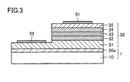
- a semiconductor device (LED) was fabricated in the following manner, by using each GaN layer bonded substrate (group III nitride semiconductor layer bonded substrate 1) manufactured in each of Comparative Example 1 and Examples 1 and 3.
- n-type GaN layer 31 was partially exposed by mesa etching. Thereafter, with vacuum evaporation or electron beam evaporation, a p-side electrode 51 was formed on p-type GaN layer 35 and an n-side electrode 52 was formed on n-type GaN layer 31 of which surface was exposed.
- a semiconductor device including the GaN layer bonded substrate in Comparative Example 1 is referred to as a semiconductor device according to Comparative Example 1
- a semiconductor device including the GaN layer bonded substrate in Example 1 is referred to as a semiconductor device according to Example 1
- a semiconductor device including the GaN layer bonded substrate in Example 3 is referred to as a semiconductor device according to Example 3.
Claims (5)
- Procédé de fabrication d'un substrat fixé à une couche de semi-conducteur de nitrure de groupe III dans lequel une couche de semi-conducteur de nitrure de groupe III (20a) et un substrat de composition différente (10) diffèrent en termes de composition chimique de ladite couche de semi-conducteur de nitrure de groupe III (20a) sont fixés l'un à l'autre, comprenant les étapes consistant à :implanter des ions d'au moins l'un quelconque de l'hydrogène et l'hélium dans une région ayant une production prescrite depuis une surface principale (20 m) d'un substrat de semi-conducteur de nitrure de groupe III (20) ;fixer ledit substrat de composition différente (10) avec ladite surface principale (20m) dudit substrat de semi-conducteur de nitrure de groupe III (20) ;obtenir ledit substrat fixé à une couche de semi-conducteur de nitrure de groupe III (1) par séparation dudit substrat de semi-conducteur de nitrure de groupe III (20) au niveau de ladite région (20i) implantée avec lesdits ions ; caractérisé parle recuit dudit substrat fixé à une couche de semi-conducteur de nitrure de groupe III (1) à une température d'au moins 700 °C dans une atmosphère d'un gaz contenant de l'azote.
- Procédé de fabrication d'un substrat fixé à une couche de semi-conducteur de nitrure de groupe III selon la revendication 1, dans lequel ledit gaz contenant de l'azote comprend un gaz d'ammoniac.
- Procédé de fabrication d'un substrat fixé à une couche de semi-conducteur de nitrure de groupe III selon la revendication 1, dans lequel ladite étape de recuit est effectuée à une température d'au moins 950 °C.
- Procédé de fabrication d'un substrat fixé à une couche de semi-conducteur de nitrure de groupe III selon la revendication 1, comprenant en outre l'étape consistant à enlever ladite région (20i) implantée avec lesdits ions dans ladite couche de semi-conducteur de nitrure de groupe III (20a) après ladite étape d'obtention dudit substrat fixé à une couche de semi-conducteur de nitrure de groupe III (1) et avant ladite étape de recuit.
- Procédé de fabrication d'un substrat fixé à une couche de semi-conducteur de nitrure de groupe III selon la revendication 1, dans lequel une demi-largeur de pic de diffraction des rayons X dans une courbe oscillante associée à un plan (0002) de ladite couche de semi-conducteur de nitrure de groupe III (20a) dudit substrat fixé à une couche de semi-conducteur de nitrure de groupe III (1) après ledit recuit est de 450 arcsecondes ou moins.
Applications Claiming Priority (1)
| Application Number | Priority Date | Filing Date | Title |
|---|---|---|---|
| JP2008206933A JP4631946B2 (ja) | 2008-08-11 | 2008-08-11 | Iii族窒化物半導体層貼り合わせ基板の製造方法 |
Publications (3)
| Publication Number | Publication Date |
|---|---|
| EP2154709A2 EP2154709A2 (fr) | 2010-02-17 |
| EP2154709A3 EP2154709A3 (fr) | 2010-09-01 |
| EP2154709B1 true EP2154709B1 (fr) | 2011-09-21 |
Family
ID=41263649
Family Applications (1)
| Application Number | Title | Priority Date | Filing Date |
|---|---|---|---|
| EP09166067A Not-in-force EP2154709B1 (fr) | 2008-08-11 | 2009-07-22 | Procédé de fabrication de substrat lié à couche de semi-conducteur de nitrure de groupe III |
Country Status (7)
| Country | Link |
|---|---|
| US (1) | US8124498B2 (fr) |
| EP (1) | EP2154709B1 (fr) |
| JP (1) | JP4631946B2 (fr) |
| KR (1) | KR20100019965A (fr) |
| CN (1) | CN101651091A (fr) |
| AT (1) | ATE525744T1 (fr) |
| TW (1) | TW201006974A (fr) |
Families Citing this family (13)
| Publication number | Priority date | Publication date | Assignee | Title |
|---|---|---|---|---|
| US9064706B2 (en) * | 2006-11-17 | 2015-06-23 | Sumitomo Electric Industries, Ltd. | Composite of III-nitride crystal on laterally stacked substrates |
| JP5544875B2 (ja) * | 2009-12-25 | 2014-07-09 | 住友電気工業株式会社 | 複合基板 |
| US8916399B2 (en) * | 2010-04-08 | 2014-12-23 | Nichia Corporation | Method of manufacturing light emitting device including light emitting element and wavelength converting member |
| EP2562789A4 (fr) | 2010-04-20 | 2015-03-04 | Sumitomo Electric Industries | Procédé de production d'un substrat composite |
| RU2550771C2 (ru) | 2010-05-31 | 2015-05-10 | Нития Корпорейшн | Светоизлучающее устройство и способ изготовления светоизлучающего устройства |
| CN101962804B (zh) * | 2010-10-30 | 2012-05-02 | 北京大学 | 基于外延材料应力控制的GaN厚膜自分离方法 |
| JP2012124473A (ja) | 2010-11-15 | 2012-06-28 | Ngk Insulators Ltd | 複合基板及び複合基板の製造方法 |
| CN104641453B (zh) * | 2012-10-12 | 2018-03-30 | 住友电气工业株式会社 | Iii族氮化物复合衬底及其制造方法以及制造iii族氮化物半导体器件的方法 |
| US9281233B2 (en) * | 2012-12-28 | 2016-03-08 | Sunedison Semiconductor Limited | Method for low temperature layer transfer in the preparation of multilayer semiconductor devices |
| US9058990B1 (en) * | 2013-12-19 | 2015-06-16 | International Business Machines Corporation | Controlled spalling of group III nitrides containing an embedded spall releasing plane |
| CN103696022B (zh) * | 2013-12-27 | 2016-04-13 | 贵州蓝科睿思技术研发中心 | 一种离子注入分离蓝宝石的方法 |
| JP6268229B2 (ja) * | 2016-06-27 | 2018-01-24 | 株式会社サイオクス | 窒化物半導体積層物、窒化物半導体積層物の製造方法、半導体積層物の製造方法、および半導体積層物の検査方法 |
| CN113808925A (zh) * | 2021-09-28 | 2021-12-17 | 包头稀土研发中心 | 一种复合结构荧光衬底、复合方法及倒装led结构 |
Family Cites Families (6)
| Publication number | Priority date | Publication date | Assignee | Title |
|---|---|---|---|---|
| JP3658756B2 (ja) * | 1999-03-01 | 2005-06-08 | 住友電気工業株式会社 | 化合物半導体の製造方法 |
| PL207400B1 (pl) * | 2001-06-06 | 2010-12-31 | Ammono Społka Z Ograniczoną Odpowiedzialnością | Sposób i urządzenie do otrzymywania objętościowego monokryształu azotku zawierającego gal |
| JP2006210660A (ja) * | 2005-01-28 | 2006-08-10 | Hitachi Cable Ltd | 半導体基板の製造方法 |
| JP5003033B2 (ja) * | 2006-06-30 | 2012-08-15 | 住友電気工業株式会社 | GaN薄膜貼り合わせ基板およびその製造方法、ならびにGaN系半導体デバイスおよびその製造方法 |
| US7575988B2 (en) * | 2006-07-11 | 2009-08-18 | S.O.I.Tec Silicon On Insulator Technologies | Method of fabricating a hybrid substrate |
| JP2008159692A (ja) * | 2006-12-21 | 2008-07-10 | Covalent Materials Corp | 半導体基板の製造方法 |
-
2008
- 2008-08-11 JP JP2008206933A patent/JP4631946B2/ja active Active
-
2009
- 2009-07-22 AT AT09166067T patent/ATE525744T1/de not_active IP Right Cessation
- 2009-07-22 EP EP09166067A patent/EP2154709B1/fr not_active Not-in-force
- 2009-07-28 TW TW098125392A patent/TW201006974A/zh unknown
- 2009-08-04 US US12/535,201 patent/US8124498B2/en active Active
- 2009-08-06 KR KR1020090072400A patent/KR20100019965A/ko not_active Application Discontinuation
- 2009-08-11 CN CN200910166065A patent/CN101651091A/zh active Pending
Also Published As
| Publication number | Publication date |
|---|---|
| KR20100019965A (ko) | 2010-02-19 |
| US8124498B2 (en) | 2012-02-28 |
| EP2154709A2 (fr) | 2010-02-17 |
| TW201006974A (en) | 2010-02-16 |
| ATE525744T1 (de) | 2011-10-15 |
| CN101651091A (zh) | 2010-02-17 |
| US20100035406A1 (en) | 2010-02-11 |
| JP4631946B2 (ja) | 2011-02-16 |
| JP2010045098A (ja) | 2010-02-25 |
| EP2154709A3 (fr) | 2010-09-01 |
Similar Documents
| Publication | Publication Date | Title |
|---|---|---|
| EP2154709B1 (fr) | Procédé de fabrication de substrat lié à couche de semi-conducteur de nitrure de groupe III | |
| JP4458116B2 (ja) | エピタキシャル層成長用iii族窒化物半導体層貼り合わせ基板および半導体デバイス | |
| EP1873817B1 (fr) | Substrat ayant une couche mince de GaN assemblée et son procédé de fabrication | |
| JP5407385B2 (ja) | 複合基板、エピタキシャル基板、半導体デバイス及び複合基板の製造方法 | |
| US8884306B2 (en) | Semiconductor device and method for manufacturing the same | |
| JP5765037B2 (ja) | 複合基板の製造方法 | |
| US10186451B2 (en) | Group III nitride composite substrate and method for manufacturing the same, and method for manufacturing group III nitride semiconductor device | |
| US8748890B2 (en) | Method of manufacturing semiconductor wafer, and composite base and composite substrate for use in that method | |
| US7537944B2 (en) | Method for manufacturing p-type group III nitride semiconductor, and group III nitride semiconductor light-emitting device | |
| WO2010089928A1 (fr) | SUBSTRAT DE GaN, PROCÉDÉ POUR LA FABRICATION D'UN SUBSTRAT DE GaN, PROCÉDÉ POUR LA FABRICATION D'UN SUBSTRAT COLLÉ À UNE COUCHE DE GaN ET PROCÉDÉ POUR LA FABRICATION D'UN DISPOSITIF À SEMI-CONDUCTEUR | |
| JP5682651B2 (ja) | 半導体デバイス及びその製造方法 | |
| JP2010226023A (ja) | 窒化物系化合物半導体層を支持基板上に有する基板生産物を製造する方法、及び半導体デバイスの製造方法 | |
| JP5598321B2 (ja) | 半導体デバイスの製造方法 | |
| JP2009260391A (ja) | Iii族窒化物半導体層貼り合わせ基板および半導体デバイスの製造方法 | |
| KR102342876B1 (ko) | 2d박막 삽입층을 이용한 이종접합 다이오드 및 이의 제조방법 | |
| JP2011176322A (ja) | GaN基板およびその製造方法、GaN層接合基板の製造方法、ならびに半導体デバイスの製造方法 | |
| JP5544875B2 (ja) | 複合基板 | |
| JP2011044665A (ja) | Iii族窒化物半導体層接合基板およびiii族窒化物半導体デバイスの製造方法 | |
| JP2010192698A (ja) | イオン注入iii族窒化物半導体基板、iii族窒化物半導体層接合基板およびiii族窒化物半導体デバイスの製造方法 |
Legal Events
| Date | Code | Title | Description |
|---|---|---|---|
| PUAI | Public reference made under article 153(3) epc to a published international application that has entered the european phase |
Free format text: ORIGINAL CODE: 0009012 |
|
| AK | Designated contracting states |
Kind code of ref document: A2 Designated state(s): AT BE BG CH CY CZ DE DK EE ES FI FR GB GR HR HU IE IS IT LI LT LU LV MC MK MT NL NO PL PT RO SE SI SK SM TR |
|
| AX | Request for extension of the european patent |
Extension state: AL BA RS |
|
| PUAL | Search report despatched |
Free format text: ORIGINAL CODE: 0009013 |
|
| AK | Designated contracting states |
Kind code of ref document: A3 Designated state(s): AT BE BG CH CY CZ DE DK EE ES FI FR GB GR HR HU IE IS IT LI LT LU LV MC MK MT NL NO PL PT RO SE SI SK SM TR |
|
| AX | Request for extension of the european patent |
Extension state: AL BA RS |
|
| PUAF | Information related to the publication of a search report (a3 document) modified or deleted |
Free format text: ORIGINAL CODE: 0009199SEPU |
|
| PUAL | Search report despatched |
Free format text: ORIGINAL CODE: 0009013 |
|
| D17D | Deferred search report published (deleted) | ||
| AK | Designated contracting states |
Kind code of ref document: A3 Designated state(s): AT BE BG CH CY CZ DE DK EE ES FI FR GB GR HR HU IE IS IT LI LT LU LV MC MK MT NL NO PL PT RO SE SI SK SM TR |
|
| AX | Request for extension of the european patent |
Extension state: AL BA RS |
|
| 17P | Request for examination filed |
Effective date: 20101112 |
|
| RIC1 | Information provided on ipc code assigned before grant |
Ipc: H01L 21/18 20060101AFI20110207BHEP Ipc: H01L 33/00 20100101ALN20110207BHEP |
|
| GRAP | Despatch of communication of intention to grant a patent |
Free format text: ORIGINAL CODE: EPIDOSNIGR1 |
|
| GRAS | Grant fee paid |
Free format text: ORIGINAL CODE: EPIDOSNIGR3 |
|
| GRAA | (expected) grant |
Free format text: ORIGINAL CODE: 0009210 |
|
| AK | Designated contracting states |
Kind code of ref document: B1 Designated state(s): AT BE BG CH CY CZ DE DK EE ES FI FR GB GR HR HU IE IS IT LI LT LU LV MC MK MT NL NO PL PT RO SE SI SK SM TR |
|
| REG | Reference to a national code |
Ref country code: GB Ref legal event code: FG4D |
|
| REG | Reference to a national code |
Ref country code: CH Ref legal event code: EP |
|
| REG | Reference to a national code |
Ref country code: IE Ref legal event code: FG4D |
|
| REG | Reference to a national code |
Ref country code: DE Ref legal event code: R096 Ref document number: 602009002662 Country of ref document: DE Effective date: 20111117 |
|
| REG | Reference to a national code |
Ref country code: DE Ref legal event code: R082 Ref document number: 602009002662 Country of ref document: DE Representative=s name: GRUENECKER, KINKELDEY, STOCKMAIR & SCHWANHAEUS, DE |
|
| REG | Reference to a national code |
Ref country code: NL Ref legal event code: VDEP Effective date: 20110921 |
|
| PG25 | Lapsed in a contracting state [announced via postgrant information from national office to epo] |
Ref country code: SE Free format text: LAPSE BECAUSE OF FAILURE TO SUBMIT A TRANSLATION OF THE DESCRIPTION OR TO PAY THE FEE WITHIN THE PRESCRIBED TIME-LIMIT Effective date: 20110921 Ref country code: HR Free format text: LAPSE BECAUSE OF FAILURE TO SUBMIT A TRANSLATION OF THE DESCRIPTION OR TO PAY THE FEE WITHIN THE PRESCRIBED TIME-LIMIT Effective date: 20110921 Ref country code: FI Free format text: LAPSE BECAUSE OF FAILURE TO SUBMIT A TRANSLATION OF THE DESCRIPTION OR TO PAY THE FEE WITHIN THE PRESCRIBED TIME-LIMIT Effective date: 20110921 Ref country code: LT Free format text: LAPSE BECAUSE OF FAILURE TO SUBMIT A TRANSLATION OF THE DESCRIPTION OR TO PAY THE FEE WITHIN THE PRESCRIBED TIME-LIMIT Effective date: 20110921 Ref country code: NO Free format text: LAPSE BECAUSE OF FAILURE TO SUBMIT A TRANSLATION OF THE DESCRIPTION OR TO PAY THE FEE WITHIN THE PRESCRIBED TIME-LIMIT Effective date: 20111221 |
|
| LTIE | Lt: invalidation of european patent or patent extension |
Effective date: 20110921 |
|
| PG25 | Lapsed in a contracting state [announced via postgrant information from national office to epo] |
Ref country code: SI Free format text: LAPSE BECAUSE OF FAILURE TO SUBMIT A TRANSLATION OF THE DESCRIPTION OR TO PAY THE FEE WITHIN THE PRESCRIBED TIME-LIMIT Effective date: 20110921 Ref country code: AT Free format text: LAPSE BECAUSE OF FAILURE TO SUBMIT A TRANSLATION OF THE DESCRIPTION OR TO PAY THE FEE WITHIN THE PRESCRIBED TIME-LIMIT Effective date: 20110921 Ref country code: LV Free format text: LAPSE BECAUSE OF FAILURE TO SUBMIT A TRANSLATION OF THE DESCRIPTION OR TO PAY THE FEE WITHIN THE PRESCRIBED TIME-LIMIT Effective date: 20110921 Ref country code: GR Free format text: LAPSE BECAUSE OF FAILURE TO SUBMIT A TRANSLATION OF THE DESCRIPTION OR TO PAY THE FEE WITHIN THE PRESCRIBED TIME-LIMIT Effective date: 20111222 Ref country code: CY Free format text: LAPSE BECAUSE OF FAILURE TO SUBMIT A TRANSLATION OF THE DESCRIPTION OR TO PAY THE FEE WITHIN THE PRESCRIBED TIME-LIMIT Effective date: 20110921 |
|
| REG | Reference to a national code |
Ref country code: AT Ref legal event code: MK05 Ref document number: 525744 Country of ref document: AT Kind code of ref document: T Effective date: 20110921 |
|
| PG25 | Lapsed in a contracting state [announced via postgrant information from national office to epo] |
Ref country code: BE Free format text: LAPSE BECAUSE OF FAILURE TO SUBMIT A TRANSLATION OF THE DESCRIPTION OR TO PAY THE FEE WITHIN THE PRESCRIBED TIME-LIMIT Effective date: 20110921 |
|
| PG25 | Lapsed in a contracting state [announced via postgrant information from national office to epo] |
Ref country code: CZ Free format text: LAPSE BECAUSE OF FAILURE TO SUBMIT A TRANSLATION OF THE DESCRIPTION OR TO PAY THE FEE WITHIN THE PRESCRIBED TIME-LIMIT Effective date: 20110921 Ref country code: SK Free format text: LAPSE BECAUSE OF FAILURE TO SUBMIT A TRANSLATION OF THE DESCRIPTION OR TO PAY THE FEE WITHIN THE PRESCRIBED TIME-LIMIT Effective date: 20110921 Ref country code: IS Free format text: LAPSE BECAUSE OF FAILURE TO SUBMIT A TRANSLATION OF THE DESCRIPTION OR TO PAY THE FEE WITHIN THE PRESCRIBED TIME-LIMIT Effective date: 20120121 |
|
| PG25 | Lapsed in a contracting state [announced via postgrant information from national office to epo] |
Ref country code: PL Free format text: LAPSE BECAUSE OF FAILURE TO SUBMIT A TRANSLATION OF THE DESCRIPTION OR TO PAY THE FEE WITHIN THE PRESCRIBED TIME-LIMIT Effective date: 20110921 Ref country code: IT Free format text: LAPSE BECAUSE OF FAILURE TO SUBMIT A TRANSLATION OF THE DESCRIPTION OR TO PAY THE FEE WITHIN THE PRESCRIBED TIME-LIMIT Effective date: 20110921 Ref country code: EE Free format text: LAPSE BECAUSE OF FAILURE TO SUBMIT A TRANSLATION OF THE DESCRIPTION OR TO PAY THE FEE WITHIN THE PRESCRIBED TIME-LIMIT Effective date: 20110921 Ref country code: RO Free format text: LAPSE BECAUSE OF FAILURE TO SUBMIT A TRANSLATION OF THE DESCRIPTION OR TO PAY THE FEE WITHIN THE PRESCRIBED TIME-LIMIT Effective date: 20110921 Ref country code: PT Free format text: LAPSE BECAUSE OF FAILURE TO SUBMIT A TRANSLATION OF THE DESCRIPTION OR TO PAY THE FEE WITHIN THE PRESCRIBED TIME-LIMIT Effective date: 20120123 Ref country code: NL Free format text: LAPSE BECAUSE OF FAILURE TO SUBMIT A TRANSLATION OF THE DESCRIPTION OR TO PAY THE FEE WITHIN THE PRESCRIBED TIME-LIMIT Effective date: 20110921 |
|
| PLBE | No opposition filed within time limit |
Free format text: ORIGINAL CODE: 0009261 |
|
| STAA | Information on the status of an ep patent application or granted ep patent |
Free format text: STATUS: NO OPPOSITION FILED WITHIN TIME LIMIT |
|
| PG25 | Lapsed in a contracting state [announced via postgrant information from national office to epo] |
Ref country code: DK Free format text: LAPSE BECAUSE OF FAILURE TO SUBMIT A TRANSLATION OF THE DESCRIPTION OR TO PAY THE FEE WITHIN THE PRESCRIBED TIME-LIMIT Effective date: 20110921 |
|
| 26N | No opposition filed |
Effective date: 20120622 |
|
| REG | Reference to a national code |
Ref country code: DE Ref legal event code: R097 Ref document number: 602009002662 Country of ref document: DE Effective date: 20120622 |
|
| PG25 | Lapsed in a contracting state [announced via postgrant information from national office to epo] |
Ref country code: MK Free format text: LAPSE BECAUSE OF FAILURE TO SUBMIT A TRANSLATION OF THE DESCRIPTION OR TO PAY THE FEE WITHIN THE PRESCRIBED TIME-LIMIT Effective date: 20110921 Ref country code: MC Free format text: LAPSE BECAUSE OF NON-PAYMENT OF DUE FEES Effective date: 20120731 |
|
| PG25 | Lapsed in a contracting state [announced via postgrant information from national office to epo] |
Ref country code: DE Free format text: LAPSE BECAUSE OF NON-PAYMENT OF DUE FEES Effective date: 20130201 Ref country code: ES Free format text: LAPSE BECAUSE OF FAILURE TO SUBMIT A TRANSLATION OF THE DESCRIPTION OR TO PAY THE FEE WITHIN THE PRESCRIBED TIME-LIMIT Effective date: 20120101 |
|
| REG | Reference to a national code |
Ref country code: IE Ref legal event code: MM4A |
|
| PG25 | Lapsed in a contracting state [announced via postgrant information from national office to epo] |
Ref country code: BG Free format text: LAPSE BECAUSE OF FAILURE TO SUBMIT A TRANSLATION OF THE DESCRIPTION OR TO PAY THE FEE WITHIN THE PRESCRIBED TIME-LIMIT Effective date: 20111221 |
|
| PG25 | Lapsed in a contracting state [announced via postgrant information from national office to epo] |
Ref country code: MT Free format text: LAPSE BECAUSE OF FAILURE TO SUBMIT A TRANSLATION OF THE DESCRIPTION OR TO PAY THE FEE WITHIN THE PRESCRIBED TIME-LIMIT Effective date: 20110921 Ref country code: IE Free format text: LAPSE BECAUSE OF NON-PAYMENT OF DUE FEES Effective date: 20120722 |
|
| REG | Reference to a national code |
Ref country code: DE Ref legal event code: R119 Ref document number: 602009002662 Country of ref document: DE Effective date: 20130201 |
|
| REG | Reference to a national code |
Ref country code: CH Ref legal event code: PL |
|
| GBPC | Gb: european patent ceased through non-payment of renewal fee |
Effective date: 20130722 |
|
| PG25 | Lapsed in a contracting state [announced via postgrant information from national office to epo] |
Ref country code: GB Free format text: LAPSE BECAUSE OF NON-PAYMENT OF DUE FEES Effective date: 20130722 Ref country code: CH Free format text: LAPSE BECAUSE OF NON-PAYMENT OF DUE FEES Effective date: 20130731 Ref country code: TR Free format text: LAPSE BECAUSE OF FAILURE TO SUBMIT A TRANSLATION OF THE DESCRIPTION OR TO PAY THE FEE WITHIN THE PRESCRIBED TIME-LIMIT Effective date: 20110921 Ref country code: LI Free format text: LAPSE BECAUSE OF NON-PAYMENT OF DUE FEES Effective date: 20130731 |
|
| PG25 | Lapsed in a contracting state [announced via postgrant information from national office to epo] |
Ref country code: SM Free format text: LAPSE BECAUSE OF FAILURE TO SUBMIT A TRANSLATION OF THE DESCRIPTION OR TO PAY THE FEE WITHIN THE PRESCRIBED TIME-LIMIT Effective date: 20110921 Ref country code: LU Free format text: LAPSE BECAUSE OF NON-PAYMENT OF DUE FEES Effective date: 20120722 |
|
| PG25 | Lapsed in a contracting state [announced via postgrant information from national office to epo] |
Ref country code: HU Free format text: LAPSE BECAUSE OF FAILURE TO SUBMIT A TRANSLATION OF THE DESCRIPTION OR TO PAY THE FEE WITHIN THE PRESCRIBED TIME-LIMIT Effective date: 20090722 |
|
| REG | Reference to a national code |
Ref country code: FR Ref legal event code: PLFP Year of fee payment: 8 |
|
| REG | Reference to a national code |
Ref country code: FR Ref legal event code: PLFP Year of fee payment: 9 |
|
| PGFP | Annual fee paid to national office [announced via postgrant information from national office to epo] |
Ref country code: FR Payment date: 20170613 Year of fee payment: 9 |
|
| PG25 | Lapsed in a contracting state [announced via postgrant information from national office to epo] |
Ref country code: FR Free format text: LAPSE BECAUSE OF NON-PAYMENT OF DUE FEES Effective date: 20180731 |