EP2139304A1 - Bestücktes Substrat und elektronische Vorrichtung - Google Patents
Bestücktes Substrat und elektronische Vorrichtung Download PDFInfo
- Publication number
- EP2139304A1 EP2139304A1 EP09152045A EP09152045A EP2139304A1 EP 2139304 A1 EP2139304 A1 EP 2139304A1 EP 09152045 A EP09152045 A EP 09152045A EP 09152045 A EP09152045 A EP 09152045A EP 2139304 A1 EP2139304 A1 EP 2139304A1
- Authority
- EP
- European Patent Office
- Prior art keywords
- printed substrate
- hole
- polygonal shape
- bump
- package
- Prior art date
- Legal status (The legal status is an assumption and is not a legal conclusion. Google has not performed a legal analysis and makes no representation as to the accuracy of the status listed.)
- Withdrawn
Links
Images





Classifications
-
- H—ELECTRICITY
- H05—ELECTRIC TECHNIQUES NOT OTHERWISE PROVIDED FOR
- H05K—PRINTED CIRCUITS; CASINGS OR CONSTRUCTIONAL DETAILS OF ELECTRIC APPARATUS; MANUFACTURE OF ASSEMBLAGES OF ELECTRICAL COMPONENTS
- H05K1/00—Printed circuits
- H05K1/02—Details
-
- H—ELECTRICITY
- H05—ELECTRIC TECHNIQUES NOT OTHERWISE PROVIDED FOR
- H05K—PRINTED CIRCUITS; CASINGS OR CONSTRUCTIONAL DETAILS OF ELECTRIC APPARATUS; MANUFACTURE OF ASSEMBLAGES OF ELECTRICAL COMPONENTS
- H05K1/00—Printed circuits
- H05K1/02—Details
- H05K1/0271—Arrangements for reducing stress or warp in rigid printed circuit boards, e.g. caused by loads, vibrations or differences in thermal expansion
-
- H—ELECTRICITY
- H05—ELECTRIC TECHNIQUES NOT OTHERWISE PROVIDED FOR
- H05K—PRINTED CIRCUITS; CASINGS OR CONSTRUCTIONAL DETAILS OF ELECTRIC APPARATUS; MANUFACTURE OF ASSEMBLAGES OF ELECTRICAL COMPONENTS
- H05K1/00—Printed circuits
- H05K1/18—Printed circuits structurally associated with non-printed electric components
-
- H—ELECTRICITY
- H05—ELECTRIC TECHNIQUES NOT OTHERWISE PROVIDED FOR
- H05K—PRINTED CIRCUITS; CASINGS OR CONSTRUCTIONAL DETAILS OF ELECTRIC APPARATUS; MANUFACTURE OF ASSEMBLAGES OF ELECTRICAL COMPONENTS
- H05K3/00—Apparatus or processes for manufacturing printed circuits
- H05K3/30—Assembling printed circuits with electric components, e.g. with resistors
- H05K3/32—Assembling printed circuits with electric components, e.g. with resistors electrically connecting electric components or wires to printed circuits
-
- H—ELECTRICITY
- H05—ELECTRIC TECHNIQUES NOT OTHERWISE PROVIDED FOR
- H05K—PRINTED CIRCUITS; CASINGS OR CONSTRUCTIONAL DETAILS OF ELECTRIC APPARATUS; MANUFACTURE OF ASSEMBLAGES OF ELECTRICAL COMPONENTS
- H05K3/00—Apparatus or processes for manufacturing printed circuits
- H05K3/30—Assembling printed circuits with electric components, e.g. with resistors
- H05K3/32—Assembling printed circuits with electric components, e.g. with resistors electrically connecting electric components or wires to printed circuits
- H05K3/34—Assembling printed circuits with electric components, e.g. with resistors electrically connecting electric components or wires to printed circuits by soldering
-
- H—ELECTRICITY
- H05—ELECTRIC TECHNIQUES NOT OTHERWISE PROVIDED FOR
- H05K—PRINTED CIRCUITS; CASINGS OR CONSTRUCTIONAL DETAILS OF ELECTRIC APPARATUS; MANUFACTURE OF ASSEMBLAGES OF ELECTRICAL COMPONENTS
- H05K2201/00—Indexing scheme relating to printed circuits covered by H05K1/00
- H05K2201/09—Shape and layout
- H05K2201/09009—Substrate related
- H05K2201/09063—Holes or slots in insulating substrate not used for electrical connections
-
- Y—GENERAL TAGGING OF NEW TECHNOLOGICAL DEVELOPMENTS; GENERAL TAGGING OF CROSS-SECTIONAL TECHNOLOGIES SPANNING OVER SEVERAL SECTIONS OF THE IPC; TECHNICAL SUBJECTS COVERED BY FORMER USPC CROSS-REFERENCE ART COLLECTIONS [XRACs] AND DIGESTS
- Y10—TECHNICAL SUBJECTS COVERED BY FORMER USPC
- Y10T—TECHNICAL SUBJECTS COVERED BY FORMER US CLASSIFICATION
- Y10T428/00—Stock material or miscellaneous articles
- Y10T428/24—Structurally defined web or sheet [e.g., overall dimension, etc.]
- Y10T428/24273—Structurally defined web or sheet [e.g., overall dimension, etc.] including aperture
- Y10T428/24322—Composite web or sheet
Definitions
- the present invention is related to a printed substrate that is provided with a plural pads and an electronic device with the printed substrate.
- the solder bump may be peeled off from the printed substrate, resulting in an electrical connection failure.
- Embodiments of the invention may provide a printed substrate and an electronic device, thereby preventing an electrical connection failure.
- a printed substrate includes: a plurality of pads provided in a mounting area, and having a polygonal shape, in which an electronic component is mounted; and a hole facing and extending along at least two adjacent sides of the polygonal shape.
- the concentration of the load on the solder bump which is arranged at a corner portion defined by two adjacent sides of the polygonal shape, is prevented. Therefore, the peeling of the solder bump and the printed substrate is prevented, and the electronic connection failure of the electronic component and the printed substrate can be prevented.
- FIGs. 1A to 1C illustrate a notebook-size personal computer 1 (hereinafter referred to as a notebook computer) corresponding to a portable electronic device.
- FIG. 1A is a front view of the notebook computer 1
- FIG. 1B is a side view of the notebook computer 1
- FIG. 1C is a bottom view of the notebook computer 1.
- the notebook computer 1 includes a display portion 10 and a main portion 20.
- the display portion 10 is coupled to the main portion 20 by hinge (not illustrated) so as to be openable and closable.
- FIGs. 1A to 1C illustrate the notebook computer 1 in which the display portion 10 is closed.
- a display (not illustrated) is provided on a surface, facing the main portion 20, of the display portion 10.
- a keyboard (not illustrated) is provided on a surface, facing the display portion 10, of the main portion 20.
- a tray 21 for inserting and removing a CD (Compact Disk), a DVD (Digital Versatile Disk) , and the like, is provided on the right side of the main portion 20.
- air holes 23 are provided for cooling the inside of the main portion 20.
- the housing of the main portion 20 of the notebook computer 1 houses a printed substrate 30 mentioned below.
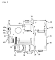
- FIGs. 2 and 3 illustrate the printed substrate 30 provided in the notebook computer 1.
- FIG. 2 illustrates a front surface of the printed substrate 30.
- FIG. 3 illustrates a rear surface of the printed substrate 30.
- the printed substrate 30 is a motherboard of the notebook computer 1.
- An external monitor connector 40a, a headphone connector 40b, and a microphone connector 40c are mounted on the front surface of the printed substrate 30.
- a USB (Universal Serial Bus) connector 40d, a CPU (Central Processing Unit) 45, a memory slot 80 and the like are mounted on the front surface of the printed substrate 30.
- Plural holes 38 are formed in the printed substrate 30.
- a semiconductor package (hereinafter, referred to as a package) 50 having the BGA (Ball Grid Array) structure, an IHC (I/O Controller Hub) 60 are provided on the rear surface of the printed substrate 30. Additionally, a hard disk 70 is mounted on both surface of the printed substrate 30.
- the CPU 45 controls the entire operation of the notebook computer 1.
- the hard disk 70 stores various programs, data, and the like.
- the memory slot 80 is provided for mounting a memory module such as a RAM (Random Access Memory) on the printed substrate 30.
- the holes 38 are provided for fixing the printed substrate 30 within the housing of the main portion 20 by screws. Thus, the printed substrate 30 is secured in the main portion 20.
- the package 50 has a square shape, and may have a rectangular shape. The square shape and the rectangular shape correspond to the polygonal shape.
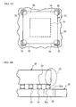
- FIGs. 4A and 4B are explanatory views of the package 50.
- FIG. 4A is an enlarged view of the package 50 mounted on the printed substrate 30.
- FIG. 4B is a side view of the package 50.
- the package 50 corresponds to an electrical component.
- a semiconductor chip 51 is built in the package 50. Additionally, plural pads 52 are provided on a bottom surface of the package 50 in a grid pattern. Solder bump (hereinafter referred to as a bump) 53 is bonded to the pad 52. Plural pads 32 bonded to the bumps 53 are provided on the printed substrate 30. The semiconductor chip 51 is electrically connected with the pad 52 via wires (not illustrates). A wiring pattern electrically connecting with the pads 32 are provided on the printed substrate 30. As mentioned above, the electrical connection of the package 50 and the printed substrate 30 is ensured.
- the hole 35 has an oblong hole shape along the shape of the corner portion 55 of the package 50, and has a substantially L shape along two adjacent sides of an outer periphery of the package 50.
- the hole 35 penetrates though the printed substrate 30.
- the holes 35 are formed by routing.
- FIG. 5 is an enlarged view of a mounting area 30R of the package 50 before the package 50 is mounted.
- the mounting area 30R has a square shape.
- the square shape corresponds to the polygonal shape.
- the plural pads 32 are provided in the mounting area 30R.
- the holes 35 respectively face the four 35R of the mounting area 30R.
- the hole 35 faces pad 32a, which is one of the plural pads 32 provided in the mounting area 30R and which is arranged closest to a corner of the mounting area 30R.
- some of the pads 32 are omitted in FIG. 5 .
- each pad may have a circular shape and a rectangular shape.
- the four holes 35 are provided to be each extending along two adjacent sides of the mounting area 30R.
- the four holes 35 includes a first hole extending along a first side and a second side of the polygonal shape of the mounting area 30R; and a second hole extending along a third side and a fourth side of the polygonal shape of the mounting area 30R.
- the four holes 35 includes a third hole extending along the first side and the fourth side of the polygonal shape; and a fourth hole extending along the second side and the third side of the polygonal shape.
- the first side and the third side of the polygonal shape oppose to each other
- the second side and the fourth side of the polygonal shape oppose to each other.
- these four holes 35 are apart from one another.
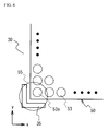
- FIG. 6 is an enlarged view of the corner portion 55.
- the hole 35 is formed to surround the bump 53a, which is arranged closest to a corner of the package 50 and which is one of the bumps 53. Additionally, some of the bumps 53 are omitted in FIG. 6 .
- FIG. 7 is a comparative view of a maximum value of von Mises stress of a printed substrate that is provided with no holes such as holes 35 and the printed substrate 30 according to the present embodiment.
- the maximum value of von Mises stress in a corner portion of the package 50 namely, in a position corresponding to the bump 53a is calculated by a simulation.
- the maximum value of von Mises stress of the printed substrate that dose not provided with the hole 35 is 132.1 MPa.
- the maximum value of von Mises stress of the printed substrate according to the present embodiment is 116.3 MPa. In this manner, the hole 35 can reduce the load applied to the corner portion 55, namely, to the bump 53a.
- the bump 53 may be peeled off from the printed substrate 30 by the deformation of the printed substrate 30.
- the bump 53a which is one of the bumps 53 and which is arranged closest to a corner, will be peeled off with ease.
- the bumps 53 other than the bump 53a arranged closest to a corner the joint of the package 50 and the printed substrate 30 is maintained by the adjacent bumps 53.
- the bump 53a arranged closest to a corner since the numbers of the bumps 53 adjacent to the bump 53a is smaller, the bump 53a is considered to be peeled off with ease.
- the hole 35 is provided to face the corner portion 55, thereby reducing the load applied to the bump 53a. This prevents the bump 53a from being peeled off from the printed substrate 30. Therefore, an electrical connection of the printed substrate 30 and the package 50 is ensured, and the failure of the notebook computer 1 is prevented.
- the heat may be transmitted to the printed substrate 30, so that the printed substrate 30 may be thermally expanded in some cases.
- the CPU 45 and the hard disk 70 generate heat and the circumference thereof becomes high temperatures, so that the heat distribution of the printed substrate 30 becomes uneven.
- the CPU 45 is mounted on the front surface of the printed substrate 30, so that a temperature difference occurs between the front and rear surfaces of the printed substrate 30.
- the printed substrate 30 may be deformed such as bended by such uneven heat distribution. The load which is applied to the bump 53a and which is caused by the thermal influence may be reduced.
- the joint force may be reduced to peel the bump 53a.
- the bump 53a is peeled off.
- each of the length of the hole 35 in the y direction and in the x direction are larger than diameters of the bump 53a and the pad 32a. This reduces the concentration of the load applied to the bump 53a.
- the length of the hole 35 may be formed to reach the middle in the each side of the package 50.
- the hole 35 is made too long, the wiring pattern ensuring the electrical connection of the bumps 53 will be interrupted.
- the mounting area of the other electrical component will be smaller. Therefore, the length and the size of the hole 35 are preferably set to face the corner portion 55 in light of the wiring pattern, the mounting area, and the prevention of the peel off of the bumps 53.
- an adhesion bond is applied around the bump 53a to strengthen the joint bonding.
- the application of the adhesion bond causes the weight of the printed substrate 30 to be increased by the adhesion bond.
- the holes 35 are provided in the printed substrate 30, thereby reducing the printed substrate 30 in weight.
- the outer shape of the printed substrate 30 and the hole 35 are integrally formed by the routing, thereby improving the efficiency in the workability. The improved efficiency in the workability can reduce the manufacturing cost.
- the shape of the hole 35 is a substantially L shape and is not limited to this shape.
- the shape of the hole 35 may be a substantially C shape.
- FIG. 8 illustrates a first modification of a printed substrate 30a.
- FIG. 8 corresponds to FIG. 4A .
- two holes 35a are provided to face two corner portions 55 arranged on a diagonal line of the package 50.
- the two holes 35 includes: a first hole extending along a first side and a second side of a polygonal shape being the outer shape of the package 50; and a second hole extending along a third side and a fourth side of the polygonal shape.
- the first side and the third side oppose to each other, and the second side and the fourth side oppose to each other. In this manner, only two holes 35a are provided on the diagonal line, thereby ensuring the wiring pattern of the bump 53 and preventing the peel off of the bump 53.
- the hole 35a may be arranged at a position that is effective for the prevention of the deformation. For example, since the positions in which the printed substrate 30a is fixed within the housing of the main portion 20 by screws are preliminarily recognized, the bending amount of the printed substrate 30a at each position can be estimated. Further, the position of an electrical component generating heat is preliminarily given. Therefore, the hole 35a may be arranged at a position having a maximal value, by estimating the maximal value of the von Mises stress of the four corner portions 55.
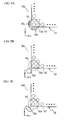
- FIG. 9A illustrates a printed substrate 30b according to a second variation.
- Two holes 35b are provided to correspond to one of the corner portions 55.
- the holes 35b are formed such that the hole 35 is divided into two by the diagonal line of the package 50.
- the holes 35b are provided along respectively two orthogonal adjacent sides. Additionally, each length of the holes 35b is larger than the diameter of the bump 53a. Referring to FIG. 9A , the hole 35b faces the bump 53a.
- the holes 35b are divided, so that the wiring pattern is formed between the holes 35b. Especially, the formation of the wiring pattern connecting with the bump 53a is facilitated.
- the holes 35b are divided into two by the diagonal line of the package 50.
- the holes are not limited to the configuration, and may be divided into two to face one of the corner portions 55.
- the wiring pattern is formed between the holes.
- FIG. 9B is a printed substrate 30c according to a third variation.
- the hole 35c has a circular shape.
- the diameter of the hole 35c is larger than that of the bump 53a. Therefore, the load applied to the bump 53a can be effectively reduced.
- FIG. 9C is a printed substrate 30d according to a fourth variation.
- the hole 35d has an elliptical shape.
- the length of the major axis of the hole 35d is larger than the diameter of the bump 53a. Therefore, the load applied to bump 53a can be effectively reduced. Additionally, the angle between the major axis of the hole 35d and one side of the package 50 is 45 degrees.
- the holes 35a to 35d according to the variations mentioned above are formed by routing.
- the shape of the hole is not limited to the above described shapes.
- the notebook computer is described as an example of the electrical device.
- the electrical device is not limited to this, and may be a desktop computer. Further, the electrical device may be a mobile phone and a portable device such as a portable external hard disk drive.
- the present invention is not limited to the BGA package, and the CSP (Chip Size Package) including a package having a size substantially identical with a semiconductor chip may be employed.
Landscapes
- Engineering & Computer Science (AREA)
- Microelectronics & Electronic Packaging (AREA)
- Manufacturing & Machinery (AREA)
- Structures For Mounting Electric Components On Printed Circuit Boards (AREA)
- Structure Of Printed Boards (AREA)
- Electric Connection Of Electric Components To Printed Circuits (AREA)
Applications Claiming Priority (1)
| Application Number | Priority Date | Filing Date | Title |
|---|---|---|---|
| JP2008168499A JP2010010428A (ja) | 2008-06-27 | 2008-06-27 | プリント基板及び電子機器 |
Publications (1)
| Publication Number | Publication Date |
|---|---|
| EP2139304A1 true EP2139304A1 (de) | 2009-12-30 |
Family
ID=40750914
Family Applications (1)
| Application Number | Title | Priority Date | Filing Date |
|---|---|---|---|
| EP09152045A Withdrawn EP2139304A1 (de) | 2008-06-27 | 2009-02-04 | Bestücktes Substrat und elektronische Vorrichtung |
Country Status (5)
| Country | Link |
|---|---|
| US (1) | US20090324885A1 (de) |
| EP (1) | EP2139304A1 (de) |
| JP (1) | JP2010010428A (de) |
| KR (1) | KR101124548B1 (de) |
| CN (2) | CN102036479A (de) |
Families Citing this family (11)
| Publication number | Priority date | Publication date | Assignee | Title |
|---|---|---|---|---|
| JP2012039033A (ja) * | 2010-08-11 | 2012-02-23 | Clarion Co Ltd | 電子回路基板、ナビゲーション装置 |
| JP5783706B2 (ja) * | 2010-11-05 | 2015-09-24 | キヤノン株式会社 | プリント回路板 |
| CN102231944A (zh) * | 2011-06-14 | 2011-11-02 | 华为技术有限公司 | 焊点应力削减结构以及包括所述结构的印刷电路板 |
| JP5879090B2 (ja) * | 2011-10-20 | 2016-03-08 | 株式会社ケーヒン | プリント配線板 |
| JP2014086920A (ja) * | 2012-10-24 | 2014-05-12 | Toshiba Corp | テレビジョン受像機、電子機器、および基板アセンブリ |
| JP5632901B2 (ja) * | 2012-11-26 | 2014-11-26 | 本田技研工業株式会社 | 端子列又は端子配列を有する電子部品が実装される回路基板 |
| JP2014229761A (ja) * | 2013-05-23 | 2014-12-08 | 株式会社東芝 | 電子機器 |
| FR3032326A1 (fr) * | 2015-02-04 | 2016-08-05 | Delphi Tech Inc | Dispositif electronique et carte de circuit imprime equipant un tel dispositif |
| CN109348618A (zh) * | 2018-12-04 | 2019-02-15 | 郑州云海信息技术有限公司 | 一种印刷电路板及系统板 |
| JP7756017B2 (ja) * | 2022-02-18 | 2025-10-17 | Astemo株式会社 | 制御装置 |
| CN115442966A (zh) * | 2022-09-29 | 2022-12-06 | 超聚变数字技术有限公司 | 电路板和电子设备 |
Citations (4)
| Publication number | Priority date | Publication date | Assignee | Title |
|---|---|---|---|---|
| DE19540814A1 (de) | 1995-11-02 | 1997-05-07 | Vdo Schindling | Platine |
| JPH1140901A (ja) | 1997-07-23 | 1999-02-12 | Sharp Corp | 回路基板 |
| US20040104041A1 (en) | 2002-11-29 | 2004-06-03 | Christensen Martin Borcher | Stress release feature for PWBs |
| US20080042276A1 (en) | 2006-08-17 | 2008-02-21 | Daryl Carvis Cromer | System and method for reducing stress-related damage to ball grid array assembly |
Family Cites Families (6)
| Publication number | Priority date | Publication date | Assignee | Title |
|---|---|---|---|---|
| US6465743B1 (en) * | 1994-12-05 | 2002-10-15 | Motorola, Inc. | Multi-strand substrate for ball-grid array assemblies and method |
| JPH08186142A (ja) * | 1994-12-28 | 1996-07-16 | Fujikura Ltd | 回路基板の構造 |
| JPH11103137A (ja) * | 1997-09-29 | 1999-04-13 | Canon Inc | フレキシブルプリント回路基板および格子状に配列された複数の接続端子を有する電子部品を実装したプリント配線基板 |
| JP4311774B2 (ja) * | 1998-03-11 | 2009-08-12 | 富士通株式会社 | 電子部品パッケージおよびプリント配線板 |
| JP2001119107A (ja) * | 1999-10-19 | 2001-04-27 | Nec Saitama Ltd | プリント配線板 |
| JP2005026501A (ja) * | 2003-07-03 | 2005-01-27 | Matsushita Electric Ind Co Ltd | 電子部品実装構造および電子部品実装方法ならびに電子部品用接着剤 |
-
2008
- 2008-06-27 JP JP2008168499A patent/JP2010010428A/ja active Pending
-
2009
- 2009-02-04 EP EP09152045A patent/EP2139304A1/de not_active Withdrawn
- 2009-02-19 KR KR1020090013871A patent/KR101124548B1/ko not_active Expired - Fee Related
- 2009-02-24 US US12/379,548 patent/US20090324885A1/en not_active Abandoned
- 2009-02-27 CN CN2011100046285A patent/CN102036479A/zh active Pending
- 2009-02-27 CN CN2009101267803A patent/CN101616543B/zh not_active Expired - Fee Related
Patent Citations (4)
| Publication number | Priority date | Publication date | Assignee | Title |
|---|---|---|---|---|
| DE19540814A1 (de) | 1995-11-02 | 1997-05-07 | Vdo Schindling | Platine |
| JPH1140901A (ja) | 1997-07-23 | 1999-02-12 | Sharp Corp | 回路基板 |
| US20040104041A1 (en) | 2002-11-29 | 2004-06-03 | Christensen Martin Borcher | Stress release feature for PWBs |
| US20080042276A1 (en) | 2006-08-17 | 2008-02-21 | Daryl Carvis Cromer | System and method for reducing stress-related damage to ball grid array assembly |
Also Published As
| Publication number | Publication date |
|---|---|
| JP2010010428A (ja) | 2010-01-14 |
| KR101124548B1 (ko) | 2012-03-21 |
| KR20100002075A (ko) | 2010-01-06 |
| CN101616543A (zh) | 2009-12-30 |
| CN102036479A (zh) | 2011-04-27 |
| CN101616543B (zh) | 2011-02-16 |
| US20090324885A1 (en) | 2009-12-31 |
Similar Documents
| Publication | Publication Date | Title |
|---|---|---|
| EP2139304A1 (de) | Bestücktes Substrat und elektronische Vorrichtung | |
| US7751918B2 (en) | Methods for configuring tubing for interconnecting in-series multiple liquid-cooled cold plates | |
| US8018722B2 (en) | Double bonded heat dissipation | |
| US7881060B2 (en) | Heat-dissipation module and electronic apparatus having the same | |
| US20070195506A1 (en) | Heat dissipating device for an integrated circuit chip | |
| US7130191B2 (en) | Function module with built-in heat dissipation device | |
| JPWO2008105069A1 (ja) | プリント基板ユニットおよび半導体パッケージ | |
| US9087814B2 (en) | Heat dissipation module | |
| US8472178B2 (en) | Memory retention system to reduce shock-related discontinuities | |
| US20160021777A1 (en) | Connector alignment system | |
| US20100007008A1 (en) | Bga package | |
| US20100038064A1 (en) | Reinforced Thermal Module Structure | |
| US20240414836A1 (en) | Heatsink based power delivery for cpus | |
| KR20100039684A (ko) | 플랙시블 반도체 패키지 및 이의 제조 방법 | |
| US11837522B2 (en) | Ball grid array package design | |
| JP6462318B2 (ja) | 半導体パッケージ | |
| US20210013155A1 (en) | Multi-metal package stiffener | |
| CN114911315B (zh) | 计算设备及计算设备的安装方法 | |
| US12213252B2 (en) | CPU for heatsink based power delivery | |
| JP6828966B2 (ja) | 基板、基板組品及び電子機器 | |
| JP6489145B2 (ja) | 電子部品及び電子部品の製造方法 | |
| KR101104380B1 (ko) | 반도체 칩 패키지, 이를 포함하는 반도체 모듈, 전자 시스템 및 반도체 칩 패키지의 제조 방법 | |
| US7492044B2 (en) | System and method for decreasing stress on solder holding BGA module to computer motherboard | |
| KR20120026774A (ko) | 메모리모듈 보호덮개 및 메모리모듈 탑재기판 | |
| JP2014130865A (ja) | 多層回路基板及び多層回路基板を備えた電子機器 |
Legal Events
| Date | Code | Title | Description |
|---|---|---|---|
| PUAI | Public reference made under article 153(3) epc to a published international application that has entered the european phase |
Free format text: ORIGINAL CODE: 0009012 |
|
| AK | Designated contracting states |
Kind code of ref document: A1 Designated state(s): AT BE BG CH CY CZ DE DK EE ES FI FR GB GR HR HU IE IS IT LI LT LU LV MC MK MT NL NO PL PT RO SE SI SK TR |
|
| AX | Request for extension of the european patent |
Extension state: AL BA RS |
|
| 17P | Request for examination filed |
Effective date: 20091223 |
|
| 17Q | First examination report despatched |
Effective date: 20100303 |
|
| AKX | Designation fees paid |
Designated state(s): DE FR GB |
|
| STAA | Information on the status of an ep patent application or granted ep patent |
Free format text: STATUS: THE APPLICATION IS DEEMED TO BE WITHDRAWN |
|
| 18D | Application deemed to be withdrawn |
Effective date: 20140624 |