EP2139107A2 - Code d'impulsions avec système de commande de moteur de modulation - Google Patents
Code d'impulsions avec système de commande de moteur de modulation Download PDFInfo
- Publication number
- EP2139107A2 EP2139107A2 EP09008134A EP09008134A EP2139107A2 EP 2139107 A2 EP2139107 A2 EP 2139107A2 EP 09008134 A EP09008134 A EP 09008134A EP 09008134 A EP09008134 A EP 09008134A EP 2139107 A2 EP2139107 A2 EP 2139107A2
- Authority
- EP
- European Patent Office
- Prior art keywords
- pcwm
- sine function
- frequency
- signal
- machine
- Prior art date
- Legal status (The legal status is an assumption and is not a legal conclusion. Google has not performed a legal analysis and makes no representation as to the accuracy of the status listed.)
- Withdrawn
Links
- 230000006870 function Effects 0.000 claims description 124
- 238000005516 engineering process Methods 0.000 claims description 14
- 238000000034 method Methods 0.000 claims description 6
- 230000005534 acoustic noise Effects 0.000 abstract description 3
- 238000010276 construction Methods 0.000 abstract description 3
- 230000000295 complement effect Effects 0.000 description 5
- 238000010586 diagram Methods 0.000 description 5
- 238000004891 communication Methods 0.000 description 2
- 230000015654 memory Effects 0.000 description 2
- 239000013078 crystal Substances 0.000 description 1
- 230000001419 dependent effect Effects 0.000 description 1
- 230000007274 generation of a signal involved in cell-cell signaling Effects 0.000 description 1
- 230000001360 synchronised effect Effects 0.000 description 1
Images


Classifications
-
- H—ELECTRICITY
- H02—GENERATION; CONVERSION OR DISTRIBUTION OF ELECTRIC POWER
- H02P—CONTROL OR REGULATION OF ELECTRIC MOTORS, ELECTRIC GENERATORS OR DYNAMO-ELECTRIC CONVERTERS; CONTROLLING TRANSFORMERS, REACTORS OR CHOKE COILS
- H02P23/00—Arrangements or methods for the control of AC motors characterised by a control method other than vector control
- H02P23/0077—Characterised by the use of a particular software algorithm
-
- H—ELECTRICITY
- H02—GENERATION; CONVERSION OR DISTRIBUTION OF ELECTRIC POWER
- H02P—CONTROL OR REGULATION OF ELECTRIC MOTORS, ELECTRIC GENERATORS OR DYNAMO-ELECTRIC CONVERTERS; CONTROLLING TRANSFORMERS, REACTORS OR CHOKE COILS
- H02P27/00—Arrangements or methods for the control of AC motors characterised by the kind of supply voltage
- H02P27/04—Arrangements or methods for the control of AC motors characterised by the kind of supply voltage using variable-frequency supply voltage, e.g. inverter or converter supply voltage
- H02P27/06—Arrangements or methods for the control of AC motors characterised by the kind of supply voltage using variable-frequency supply voltage, e.g. inverter or converter supply voltage using DC to AC converters or inverters
- H02P27/08—Arrangements or methods for the control of AC motors characterised by the kind of supply voltage using variable-frequency supply voltage, e.g. inverter or converter supply voltage using DC to AC converters or inverters with pulse width modulation
- H02P27/12—Arrangements or methods for the control of AC motors characterised by the kind of supply voltage using variable-frequency supply voltage, e.g. inverter or converter supply voltage using DC to AC converters or inverters with pulse width modulation pulsing by guiding the flux vector, current vector or voltage vector on a circle or a closed curve, e.g. for direct torque control
-
- H—ELECTRICITY
- H02—GENERATION; CONVERSION OR DISTRIBUTION OF ELECTRIC POWER
- H02P—CONTROL OR REGULATION OF ELECTRIC MOTORS, ELECTRIC GENERATORS OR DYNAMO-ELECTRIC CONVERTERS; CONTROLLING TRANSFORMERS, REACTORS OR CHOKE COILS
- H02P6/00—Arrangements for controlling synchronous motors or other dynamo-electric motors using electronic commutation dependent on the rotor position; Electronic commutators therefor
- H02P6/14—Electronic commutators
- H02P6/16—Circuit arrangements for detecting position
- H02P6/18—Circuit arrangements for detecting position without separate position detecting elements
- H02P6/185—Circuit arrangements for detecting position without separate position detecting elements using inductance sensing, e.g. pulse excitation
Definitions
- the present disclosure relates to a variable speed motor drive system, and more particularly, to a variable speed drive system employing a pulse code width modulation (PCWM) technology to be applied to drive a three phase AC motor sinusoidally without measuring rotor position.
- PCWM pulse code width modulation
- U.S. Pat. No. 4,634,952 entitled, "Inverter,” granted to Yoshino et al. (the '952 patent) describes sinusoidal motor drive signal generation by a coding method similar to one employed by Pulse Code Modulation (PCM) in a digital communication technology.
- PCM Pulse Code Modulation
- the '952 patent employs a Random Access Memory (RAM) to temporarily store the coded sinusoidal signals for the entire one signal cycle on a quasi-real time basis for the next signal output cycle. It therefore cannot alter the frequency or voltage level during the current entire signal output cycle.
- RAM Random Access Memory
- the '952 patent describes a capability to select a voltage level within the v/f envelope, it does not provide information on how to select a desired voltage level, nor does it provide any means to measure the load level of the motor.
- the '952 patent employs a synchronous signal and carrier frequency. Namely the carrier frequency range is 0.94 kHz to 1.52 kHz which is proportional to the signal frequency range.
- the '952 patent employs a complicated variable step-down counter of the basic clock frequency of 6 kHz.
- the '952 patent does not describe how to record the negative unit sine function in the Read-Only Memory (ROM).
- ROM Read-Only Memory
- U.S. Pat. No. 5,420,778 entitled, "Independent Real Time Control of Output Frequency and Voltage of PWM Inverter," granted to Yoshino (the '778 patent) also describes a coding method to generate an output PWM signal for motor drive.
- An objective of the '778 patent is an active control of an inverter output voltage using an inverter output current as the feedback signal.
- This disclosure provides a detailed architecture of PCWM technology that includes open loop control of a permanent magnet AC (PMAC) motor for, e.g., fan and compressor applications.
- PMAC permanent magnet AC
- the load level of these applications typically is known a priori. Therefore, one embodiment defines the voltage to frequency characteristic as a fixed function of the motor speed for system simplicity.
- One feature of certain embodiments is a real time calculation capability of updating an output sine function phase angle and the associated output pulse width of the PWM signal (i.e. output voltage) every constant carrier interval of approximately 51.2 ⁇ s through use of finite state machine technology.
- the concept is realized by drawing a fractional sine function circle in which an instantaneous amplitude of the fractional sine function relates directly to a pulse width numeric in a unit PWM pulse interval for the motor drive output.
- the real time calculation procedure is described in detail for one embodiment using a unit sine function table and a voltage to frequency (V/F) function table.
- Another feature of certain embodiments is a capability of carrying decimal numbers using double precision registers, thereby increasing the motor drive stability with a finer speed control.
- Yet another feature of certain embodiments is a capability of accepting the maximum output frequency and the ramp speed options from outside through a single serial communication line, thereby widening the applicability of the associated application specific integrated circuit (ASIC) to various motor drive applications.
- ASIC application specific integrated circuit
- a further feature of certain embodiments is an employment of a center modulation PWM signal which creates a power transistors' inter-conduction twice per each unit PWM pulse interval compared to once for a side modulation PWM signal, allowing a finer current waveform resulting in smoother motor drive.
- a still further feature of certain embodiments is the compactness of the associated hardware.
- the ASIC can incorporate the unit sine function table, V/F table, a clock generator, a PCWM signal encoder, and a PCWM signal decoder in one chip employing a small outline package (SOP). Additional aspects and advantages will be apparent from the following detailed description of preferred embodiments, which proceeds with reference to the accompanying drawings.
- PCWM pulse code width modulation
- the system can drive a three phase permanent magnet AC (PMAC) motor sinusoidally without sensing its rotor position.
- PMAC permanent magnet AC
- the system employs an ultrasonic carrier frequency of approximately 20 kHz to avoid acoustic noise problems. While keeping the hardware construction minimum, it can provide the highest possible motor performance and satisfy various motor operating requirements.
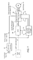
- An embodiment is explained by referring to FIG. 1 .
- An external host CPU 01 is connected to an ASIC 06 via a UART serial bus 02.
- a single phase AC line input 03 is connected to an AC to DC converter 04, of which input is then converted to a DC bus voltage 05 of approximately 150 vdc to approximately 300 vdc dependent on the system requirement.
- the ASIC 06 with the input from the UART serial bus 02, performs real time arithmetic operations and outputs gate drive input signals 07 to a gate drive and power transistor circuitry 08.
- the gate drive and power transistor circuitry 08 then outputs three sinusoidal motor drive signals 09 to drive a three phase AC motor 10.
- the DC bus voltage 05 is provided to a DC to DC step-down chopper 11 and the gate drive and power transistor circuitry 08.
- the DC to DC step-down chopper 11 produces an approximately 3.3 vdc 12 for a power supply of the ASIC 06 and an approximately 5 vdc 13 and an approximately 15 vdc 14 for a power supply of the gate drive and power transistor circuitry 08.
- FIG. 2 is a block diagram showing the detailed inside embodiment of the ASIC 06 and the gate drive and power transistor circuitry 08 according to one embodiment.
- the ASIC 06 receives its input signal via the UART serial bus 02.
- An acceleration-deceleration constant k ad and a frequency multiplication factor k fmf are input to the ASIC 06 upon a power up.
- a command frequency f c is input to the ASIC 06 as an alternate input.
- a clock generator 21 located inside the ASIC 06 working on a baseline frequency crystal oscillator of approximately 10 MHz provides various frequency clock pulses.
- a CK1 28 with the repetition period of approximately 200 ns is provided to a PCWM signal encoder 25 and a PCWM signal decoder 27.
- a CK3 29 with the repetition period of approximately 51.2 ⁇ s is provided to the PCWM signal encoder 25 and the PCWM signal decoder 27.
- a CK4 30 with the repetition period of approximately 51.2 ⁇ s is provided to the PCWM signal decoder 27.
- a CK5 31 with the repetition period of approximately 3.6864 ms is provided to the PCWM signal encoder 25.
- a unit sine function table 22 which is located inside the ASIC 06 and includes a set of maximum amplitude sine function, outputs a unit sine function numeric n u 24 back to the PCWM signal encoder 25 after receiving a unit sine function table position number n from the PCWM signal encoder 25.
- a frequency to voltage (V/F) function table 23 is located inside the ASIC 06 and outputs a machine voltage v m back to the PCWM signal encoder 25 after receiving a machine frequency f m from the PCWM signal encoder 25.
- the PCWM signal encoder 25 is located inside the ASIC 06 and includes a finite state machine which is operational on the CK1 28 clock.
- the PCWM signal encoder 25 updates the machine frequency f m and the machine voltage v m every CK5 31 interrupt period based on the acceleration-deceleration constant k ad previously supplied at the power up and a command frequency f c supplied after the power up both via the UART serial bus 02.
- the PCWM signal encoder 25 also provides PCWM numerics d 26 to the PCWM signal decoder 27 based on the updated unit sine function numeric n u corresponding to the machine frequency f m and the machine voltage v m and the frequency multiplication factor k fmf supplied via the UART serial bus 02 at the power up every CK3 29 interrupt period.
- the PCWM signal decoder 27 is located inside the ASIC 06 and comprises (see FIG.12 ) a serially connected D flip-flop 32, a 7-bit up-counter 34, and a toggle flip-flop 36 which are operational on the CK1 28 clock.
- the PCWM signal decoder 27 outputs center modulation PWM signals g 07 to the gate drive and power transistor circuitry 08 based on the PCWM numerics d 26 input from the PCWM signal encoder 25 every CK3 29 interrupt period.
- the gate drive and power transistor circuitry 08 which comprises U upper 15 and U lower 16 arms, V upper 17 and V lower 18 arms, and W upper 19 and W lower 20 arms, each pair connected in tandem to modulate the DC bus voltage 05 corresponding to the center modulation PWM signals g 07 output from the PCWM signal decoder 27, thereby applying three sinusoidal motor drive signals 09 U, V, and W to a three phase AC motor 10.
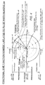
- FIG. 3 is a unit sine function table referred to by the PCWM signal encoder 25 in obtaining a unit sine function numeric n u , which is a hexa number, by inputting a unit sine function table position number n according to one embodiment.
- FIG. 4 is an illustration how the instantaneous amplitude of the fractional sine function n f can be translated into the pulse width numeric pw in the unit PWM pulse interval having 255 discrete positions according to one embodiment.
- the unit sine function circle represents a circle with the maximum radius of 127.
- Output frequency of the three sinusoidal motor drive signals 09 is proportional to the unit sine function scanning speed, which is a function of the machine frequency f m times the frequency multiplication factor k fmf .
- Output voltage of the three sinusoidal motor drive signals 09 is proportional to the fractional sine function radius which is on or inside the unit sine function circle. It is noted that when the three phase AC motor 10 starts to rotate after the power up, the corresponding rotating circle of the fractional sine function originates with the slowest rotational speed at the smallest radius near the center of the circle. Then the rotating circle moves to the outer trajectory with an accelerating speed. Finally when the three phase AC motor 10 gets to the maximum speed, the rotating circle reaches the unit sine function circle with the top rotational speed.
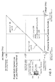
- FIG. 5 is a functional relation graph relating the pulse width numeric pw in the unit PWM pulse interval of approximately 51.2 ⁇ s to the fractional sine function numeric n f . Only integers are employed in this relation for the machine calculations. By this exact numerical relation, the instantaneous amplitude of the fractional sine function n f can be translated into the pulse width numeric pw in real time every clock CK3 29 interrupt interval of approximately 51.2 ⁇ s.
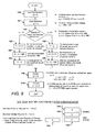
- FIG. 6 is a flow chart of a subprogram in which the machine frequency f m and the machine voltage v m are updated every CK5 31 interrupt period (approximately 3.6864ms) in S62, S66, and S68 in the PCWM signal encoder 25 according to one embodiment.
- the acceleration-deceleration constant k ad and the frequency multiplication factor k fmf in S61 are input to the PCWM signal encoder 25 via the UART serial bus 02 at the power up and stored in a frequency increment register pair D R63 and E R64 where D R63 stores null and E R64 stores an actual constant, and in a frequency multiplication factor register F R65, respectively.
- the acceleration-deceleration constant k ad can be selected externally from the outside by reflecting a ramp speed requirement for various motor drive operations. There are four ramp speed options to select.
- the frequency multiplication factor k fmf can also be selected externally from the outside by reflecting a maximum drive output frequency requirement for various motor drive applications. There are 31 maximum output frequency options to select for the gate drive and power transistor circuitry 08. S62 shows that this subprogram is entered every CK5 31 interrupt period to check if the command frequency f c which is input via the UART serial bus 02 after the power up is equal to the machine frequency f m in S63. If the command frequency f c is equal to the machine frequency f m , the subprogram goes to the exit.
- the content of frequency increment register E R64 is added to the content of machine frequency register C R62 first, followed by an addition of the content of frequency increment register D R63 and a Carry to the content of machine frequency register B R61.
- the command frequency f c is smaller than the machine frequency f m
- the content of frequency increment register E R64 is subtracted from the content of machine frequency register C R62 first, followed by a subtraction of the content of frequency increment register D R63 and a Carry from the content of content of machine frequency register B R61.
- the subprogram goes to a unit sine function table scanning speed updating subprogram.
- machine frequency register B R61 The content of machine frequency register B R61 is now stored as an updated machine frequency f m in S66.
- V/F function table 23 is entered using the updated machine frequency f m where an updated machine voltage v m is obtained and stored in a machine voltage register G R66 in S68 and the subprogram goes to exit.
- FIG. 7 is a unit sine function table scanning speed updating subprogram in which a content of a sine table position increment register pair P R74 and Q R75 is updated every CK5 31 interrupt period (approximately 3.6864ms) as shown in S62 and S75 in the PCWM signal encoder 25 according to one embodiment.
- the content of the machine frequency register pair B R61 and C R62 is loaded in a machine frequency holding register pair AH R71 and AL R72 in S71 and the content of the frequency multiplication factor register F R65, which contains k fmf , is loaded in a frequency multiplication holding register X R73 in S72.
- S75 the result obtained in S74 is loaded in the sine table position increment register pair P R74 and Q R75, and the subprogram goes to the exit.
- FIG. 8 is a flow chart of a subprogram in which the unit sine function table position n is updated every CK3 29 interrupt period (approximately 51.2 ⁇ s) as shown in S81 and S82 in the PCWM signal encoder 25 according to one embodiment.
- An addition routine in S82 is entered where the content of a unit sine function table position registers M R81, N R82, and L R83 are updated with the content of sine table position increment registers P R74 and Q R75.
- the unit sine function table position registers M R81, N R82, and L R83 and the sine table position increment register pair P R74 and Q R75 comprise double precision registers which can hold decimal point numbers until the next CK3 29 interrupt period for an enhancement of frequency control accuracy.
- a content of the sine table position increment register Q R75 is added to a content of the sine function table position register L R83 first, followed by an addition of a content of the sine table position increment register P R74 and a Carry to a content of the sine function table position register pair M R81 and N R82.
- the content of the unit sine function table position register pair M R81 and N R82 now holds an updated sine table position number n as indicated in S83.
- the unit sine function numeric n u is fetched and stored in a unit sine function register H.
- the PCWM signal encoding subprogram shown in FIG. 9 is called.
- the sine table position number n is incremented by 480 to advance the sine table position number n by 240°.
- the sine table position number n obtained in S86 is now compared with 720 in S87, and if it does not exceed 720 the subprogram goes to S89. Otherwise the subprogram proceeds to S88 where 720 is subtracted from the sine table position number n just calculated in S86 to reset the sine table position number n.
- the decimal numbers are held in registers Q R75 and L R83 until the next CK3 29 interrupt period for an enhancement of frequency control accuracy.
- the subprogram goes to S89 where it is checked whether the three sinusoidal motor drive signals 09 generation is completed. If it is not completed, the subprogram goes back to S84 and repeats the process. If it is completed the subprogram goes to exit.
- FIG. 9 is a PCWM signal encoding subprogram in which the PCWM numerics d 26 are generated every CK3 29 interrupt period (approximately 51.2 ⁇ s) as shown in S81 and S100 inside the PCWM signal encoder 25 according to one embodiment.
- the unit sine function numeric n u obtained in S84 and stored in a unit sine function register H R80 (see Fig.8 ) is loaded in a unit sine function holding register A R91 as a multiplicand.
- the machine voltage v m obtained in S68 and held in the machine voltage register G R66 is loaded in a machine voltage holding register X R92 of which content becomes a multiplier.
- the polarity of the unit sine function numeric n u is determined by checking the most significant bit of n u in S92. If it is zero or n u is positive, S93 is entered and the multiplication of AxX is performed. The upper 8 bits of the result are stored in a register A R93 and are modulated on period numeric for n u > 0. The lower 8 bits of the result are stored in a register X R94, of which content represents a decimal number of the multiplication, and is not used. In S94, h80 is added to the content of the register A R93, which becomes an overall on period numeric.
- the lower 8 bits of the result are stored in a register X R94, of which content represents a decimal number of the multiplication, and is not used.
- h80 is added to the content of the register A R93, which becomes an overall off period numeric and the subprogram proceeds to S99.
- the content of the register A R93 is a PWM side modulation off period numeric 2d for the U upper 15, V upper 17, and W upper 19 arms, respectively. If n u > 0, the output is 0 ⁇ 2d ⁇ 127 and if n u ⁇ 0, 127 ⁇ 2d ⁇ 255 will result.
- the content of the register A R93 in S99 is divided by 2 to get the PCWM numerics d 26 which comprises three PWM center modulation off period numeric for the U upper 15, V upper 17, and W upper 19 arms, respectively.
- the PCWM numerics d 26 are input to the PCWM signal decoder 27.
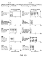
- FIG. 10 is a time chart illustrating how the PCWM numerics d 26 generated in the PCWM signal encoder 25 in FIG. 9 are converted into a pulse width numeric in the unit PWM pulse interval in the PCWM signal decoder 27 according to one embodiment.
- the illustration shows both cases where the unit sine function n u is positive and negative or zero.
- FIG. 11 is a comparison chart for the PCWM signal decoder 27 output waveforms illustrating how the side modulation and the center modulation upper arms' signals look like in the unit PWM pulse interval of approximately 51.2 ⁇ s. The comparison is made for the unit sine function n u positive, zero, and negative cases.
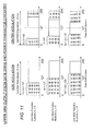
- FIG. 12 is a block diagram showing the detailed inside of the PCWM signal decoder 27 in the ASIC 06 according to one embodiment.
- the PCWM signal decoder 27 updates the center modulation PWM signals g 07 every CK3 29 interrupt period (approximately 51.2 ⁇ s).
- the center modulation PWM signals g 07 comprises three upper arms' drive signal for the upper arms 15, 17, and 19 to generate the upper arms' output signals 37 and three lower arms' drive signal for the lower arms 16, 18, and 20 to generate the lower arms' output signals 38. Both the upper and lower arms are located in the gate drive and power transistor circuitry 08.
- the PCWM signal decoder 27 receives the PCWM numerics d 26 from the PCWM signal encoder 25 and writes the data into a D Flip-Flop 32.
- the PCWM numerics d 26 represent the PWM center modulation leading-edge off period numerics for the upper arms 15, 17, and 19 in the gate drive and power transistor circuitry 08 as described in S100 of FIG. 9 and are shown in FIG. 13 .
- the lower arms 16, 18, and 20 are provided their signals from the opposite output terminal of a toggle flip-flop 36.
- a 7-bit up-counter 34 inputs the numeric d 33 from the D Flip-Flop 32 at CK3 29 and the numeric d 33 from the D Flip-Flop 32 at CK4 30 clock signals and outputs a cry signal 35 when the 7-bit up-counter 34 reaches the full count of h7f.
- the CK1 28 is used as the clock signal for the 7-bit up-counter 34 and the toggle flip-flop 36.
- the numeric d 33 is loaded for the leading edge off period generation and the d 33 for the trailing edge off period generation in the unit PWM pulse interval as depicted in FIG. 13 . Note that the 7-bit up-counter 34 loads 1's complementary numbers to generate the desired output.
- the toggle flip-flop 36 reverses the output polarity every time when it receives the cry signal 35 from the 7-bit up-counter 34 and the clocks CK3 29 or CK4 30 from the clock generator 21, and generates the three upper arms' output signals 37 and the three lower arms' output signals 38.
- the polarities of three lower arms' output signals 38 are opposite to the three upper arms' output signals 37.
- dead times between the upper and lower arms' signals 37 and 38 are omitted here.
- the center modulation PWM signals g 07 are thus generated and input to the gate drive and power transistor circuitry 08.
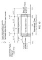
- FIG. 13 shows an example of a unit PWM pulse polarity characteristic for the upper arms' signals when the unit sine function n u is positive as a function of the normalized time in the unit PWM signal interval according to one embodiment.
- the pulse duty is more than 50% and d ⁇ 0.25.
- the modulated signal portions are split into the front-half and rear-half portions.
- FIG. 14 is a comparison chart showing that the center modulation PWM can create a power transistors' inter-conduction twice per each unit PWM pulse interval compared to once for the side modulation PWM signal according to one embodiment.
- the example chart shows the case where the U phase upper arm 15 and the V phase lower arm 18 are conducting.
Landscapes
- Engineering & Computer Science (AREA)
- Power Engineering (AREA)
- Control Of Ac Motors In General (AREA)
- Inverter Devices (AREA)
- Control Of Motors That Do Not Use Commutators (AREA)
Applications Claiming Priority (1)
| Application Number | Priority Date | Filing Date | Title |
|---|---|---|---|
| US12/145,306 US7456600B1 (en) | 2008-06-24 | 2008-06-24 | Pulse code width modulation motor drive system |
Publications (1)
| Publication Number | Publication Date |
|---|---|
| EP2139107A2 true EP2139107A2 (fr) | 2009-12-30 |
Family
ID=40029472
Family Applications (1)
| Application Number | Title | Priority Date | Filing Date |
|---|---|---|---|
| EP09008134A Withdrawn EP2139107A2 (fr) | 2008-06-24 | 2009-06-22 | Code d'impulsions avec système de commande de moteur de modulation |
Country Status (3)
| Country | Link |
|---|---|
| US (1) | US7456600B1 (fr) |
| EP (1) | EP2139107A2 (fr) |
| JP (1) | JP4482644B2 (fr) |
Cited By (1)
| Publication number | Priority date | Publication date | Assignee | Title |
|---|---|---|---|---|
| GB2578627A (en) * | 2018-11-01 | 2020-05-20 | Trw Ltd | A control system for an electric motor |
Families Citing this family (9)
| Publication number | Priority date | Publication date | Assignee | Title |
|---|---|---|---|---|
| CN103202708B (zh) * | 2012-01-13 | 2015-02-11 | 深圳市开立科技有限公司 | 一种应用于彩色超声诊断仪的高压转换方法及装置 |
| KR102080875B1 (ko) | 2013-01-23 | 2020-04-16 | 삼성디스플레이 주식회사 | 스테이지 이송 장치 및 이를 이용한 스테이지 위치 측정 방법 |
| CN105119550A (zh) * | 2015-09-24 | 2015-12-02 | 杨浩东 | 一种采用cpld实现的简易多相svpwm调制方法 |
| JP7181615B2 (ja) | 2017-10-27 | 2022-12-01 | 株式会社システム・ホームズ | 同期モータ駆動システムおよび同期モータ駆動方法 |
| US10693454B2 (en) * | 2018-05-24 | 2020-06-23 | Infineon Technologies Austria Ag | Signals for the control of power devices |
| US10784810B1 (en) * | 2019-04-29 | 2020-09-22 | Allegro Microsystems, Llc | Motor controller with accurate current measurement |
| CN112910363B (zh) * | 2021-01-22 | 2022-06-03 | 北京航空航天大学 | 一种磁悬浮永磁电机用方波与正弦波一体化控制系统 |
| US11750037B2 (en) * | 2021-06-22 | 2023-09-05 | Nucurrent, Inc. | Dynamic operation adjustment in wireless power transfer system |
| US11456627B1 (en) | 2021-06-22 | 2022-09-27 | Nucurrent, Inc. | Dynamic operation adjustment in wireless power transfer system |
Family Cites Families (14)
| Publication number | Priority date | Publication date | Assignee | Title |
|---|---|---|---|---|
| JPS5610090A (en) | 1979-07-02 | 1981-02-02 | Hitachi Ltd | Controlling device for electric motor |
| US4409534A (en) | 1980-04-09 | 1983-10-11 | General Electric Company | Microcomputer-based pulse width modulated inverter fed machine drive system |
| JPS6074996A (ja) | 1983-09-29 | 1985-04-27 | Aichi Electric Mfg Co Ltd | インバ−タの制御装置 |
| US4634952A (en) | 1983-11-30 | 1987-01-06 | System Homes Company, Ltd. | Inverter |
| JPS62236380A (ja) | 1986-04-07 | 1987-10-16 | Hitachi Seiko Ltd | Acサ−ボモ−タ制御装置 |
| JPH0356093A (ja) | 1989-07-25 | 1991-03-11 | Mitsubishi Electric Corp | 誘導電動機制御装置 |
| JP2762628B2 (ja) | 1989-11-20 | 1998-06-04 | 株式会社富士通ゼネラル | インバータ制御装置 |
| US5420778A (en) | 1990-08-09 | 1995-05-30 | System Homes Company, Ltd. | Independent real time control of output frequency and voltage of PWM inverter |
| JPH0723593A (ja) | 1993-06-30 | 1995-01-24 | Syst Hoomuzu:Kk | 周波数変換装置 |
| JPH08331893A (ja) | 1995-06-01 | 1996-12-13 | Toshiba Corp | インバータ装置 |
| JP3475727B2 (ja) | 1997-06-30 | 2003-12-08 | 松下電器産業株式会社 | インバータ装置およびインバータ制御システム装置 |
| JP4665602B2 (ja) | 2004-09-10 | 2011-04-06 | 株式会社明電舎 | 多相直列多重電力変換装置のpwm制御方法 |
| US7693244B2 (en) * | 2006-03-31 | 2010-04-06 | Intel Corporation | Encoding, clock recovery, and data bit sampling system, apparatus, and method |
| JP2007295647A (ja) | 2006-04-21 | 2007-11-08 | Meidensha Corp | インバータの同期運転方式 |
-
2008
- 2008-06-24 US US12/145,306 patent/US7456600B1/en active Active
-
2009
- 2009-05-29 JP JP2009129994A patent/JP4482644B2/ja not_active Expired - Fee Related
- 2009-06-22 EP EP09008134A patent/EP2139107A2/fr not_active Withdrawn
Cited By (2)
| Publication number | Priority date | Publication date | Assignee | Title |
|---|---|---|---|---|
| GB2578627A (en) * | 2018-11-01 | 2020-05-20 | Trw Ltd | A control system for an electric motor |
| GB2578627B (en) * | 2018-11-01 | 2023-05-03 | Trw Ltd | A control system for an electric motor |
Also Published As
| Publication number | Publication date |
|---|---|
| JP4482644B2 (ja) | 2010-06-16 |
| JP2010011728A (ja) | 2010-01-14 |
| US7456600B1 (en) | 2008-11-25 |
Similar Documents
| Publication | Publication Date | Title |
|---|---|---|
| EP2139107A2 (fr) | Code d'impulsions avec système de commande de moteur de modulation | |
| JP5178799B2 (ja) | モータ制御装置 | |
| US11056995B2 (en) | Synchronous motor drive system and synchronous motor drive method | |
| CN111525868B (zh) | 一种三相逆变器移相方法和系统以及可读存储介质 | |
| EP0821304B1 (fr) | Dispositif et méthode pour la commande par modulation de largeur d'impulsions | |
| JP6603959B2 (ja) | 多相ブラシレス直流モータ及びその駆動方法 | |
| US7449854B2 (en) | PWM signal generation apparatus and method thereof and motor control apparatus and method thereof | |
| US7436144B2 (en) | Inverter apparatus | |
| US7880428B2 (en) | Controller for induction motor | |
| WO2021014947A1 (fr) | Dispositif de commande de moteur et système de moteur | |
| JPS631835B2 (fr) | ||
| Patel et al. | A Bit-Stream based scalar control of an induction motor | |
| US20020121875A1 (en) | Method and apparatus for pulse width modulation | |
| US20020180546A1 (en) | Method for the generation of pulse-width-modulated signals and associated signal generator | |
| JPH09163759A (ja) | デジタルpwm制御装置 | |
| US6192085B1 (en) | Circuit arrangement with a data sequence generator | |
| JP2584277B2 (ja) | モータ制御回路 | |
| JPS6041548B2 (ja) | 電流形インバ−タの制御装置 | |
| Mircevski et al. | DSP application in AC drives | |
| JPS60187864A (ja) | レゾルバを用いた回転速度及び回転位置検出装置 | |
| Alhassan | Software-based position control of a permanent magnet synchronous motor | |
| JPH03151713A (ja) | Pwmパルス発生方法 | |
| JPH025052B2 (fr) | ||
| JP2007037388A (ja) | モータ駆動装置 | |
| JPS6338953B2 (fr) |
Legal Events
| Date | Code | Title | Description |
|---|---|---|---|
| PUAI | Public reference made under article 153(3) epc to a published international application that has entered the european phase |
Free format text: ORIGINAL CODE: 0009012 |
|
| AK | Designated contracting states |
Kind code of ref document: A2 Designated state(s): AT BE BG CH CY CZ DE DK EE ES FI FR GB GR HR HU IE IS IT LI LT LU LV MC MK MT NL NO PL PT RO SE SI SK TR |
|
| STAA | Information on the status of an ep patent application or granted ep patent |
Free format text: STATUS: THE APPLICATION IS DEEMED TO BE WITHDRAWN |
|
| 18D | Application deemed to be withdrawn |
Effective date: 20140103 |