EP2133732A2 - Verzögerungs-Interferometer - Google Patents
Verzögerungs-Interferometer Download PDFInfo
- Publication number
- EP2133732A2 EP2133732A2 EP09162396A EP09162396A EP2133732A2 EP 2133732 A2 EP2133732 A2 EP 2133732A2 EP 09162396 A EP09162396 A EP 09162396A EP 09162396 A EP09162396 A EP 09162396A EP 2133732 A2 EP2133732 A2 EP 2133732A2
- Authority
- EP
- European Patent Office
- Prior art keywords
- optical
- delay interferometer
- package
- phase adjusting
- glass substrate
- Prior art date
- Legal status (The legal status is an assumption and is not a legal conclusion. Google has not performed a legal analysis and makes no representation as to the accuracy of the status listed.)
- Withdrawn
Links
Images
Classifications
-
- G—PHYSICS
- G02—OPTICS
- G02B—OPTICAL ELEMENTS, SYSTEMS OR APPARATUS
- G02B6/00—Light guides; Structural details of arrangements comprising light guides and other optical elements, e.g. couplings
- G02B6/24—Coupling light guides
- G02B6/26—Optical coupling means
- G02B6/28—Optical coupling means having data bus means, i.e. plural waveguides interconnected and providing an inherently bidirectional system by mixing and splitting signals
- G02B6/293—Optical coupling means having data bus means, i.e. plural waveguides interconnected and providing an inherently bidirectional system by mixing and splitting signals with wavelength selective means
- G02B6/29379—Optical coupling means having data bus means, i.e. plural waveguides interconnected and providing an inherently bidirectional system by mixing and splitting signals with wavelength selective means characterised by the function or use of the complete device
- G02B6/29398—Temperature insensitivity
-
- G—PHYSICS
- G02—OPTICS
- G02B—OPTICAL ELEMENTS, SYSTEMS OR APPARATUS
- G02B6/00—Light guides; Structural details of arrangements comprising light guides and other optical elements, e.g. couplings
- G02B6/24—Coupling light guides
- G02B6/26—Optical coupling means
- G02B6/28—Optical coupling means having data bus means, i.e. plural waveguides interconnected and providing an inherently bidirectional system by mixing and splitting signals
- G02B6/293—Optical coupling means having data bus means, i.e. plural waveguides interconnected and providing an inherently bidirectional system by mixing and splitting signals with wavelength selective means
- G02B6/29346—Optical coupling means having data bus means, i.e. plural waveguides interconnected and providing an inherently bidirectional system by mixing and splitting signals with wavelength selective means operating by wave or beam interference
- G02B6/29349—Michelson or Michelson/Gires-Tournois configuration, i.e. based on splitting and interferometrically combining relatively delayed signals at a single beamsplitter
Definitions
- the present disclosure relates to temperature compensation of a delay interferometer.
- Patent Reference 1 discloses in detail the technique.
- Fig. 4 is a functional block diagram illustrating the operation of an optical phase adjusting plate which is used in a Michelson delay interferometer unit.
- the Michelson delay interferometer unit 500 includes a beam splitter 501 and planar mirrors 502, 503.
- the beam splitter 501 is a planar member in which a dielectric multilayer film 501b is formed on a glass substrate 501a.
- An incident light beam L500 enters the beam splitter 501 at a predetermined angle (45°).
- the beam splitter 501 reflects the incident light beam L500 and also allows to transmit therethrough to split the light beam into split light beams L501, L502 having a predetermined intensity ratio (1 : 1).
- the beam splitter 501 multiplexes the split light beams L501, L502 which are reflected respectively from the planar mirrors 502, 503, to cause the light beams to interfere with each other, and splits the interference light beam which is obtained as a result of the interference, at a predetermined intensity ratio (1 : 1).
- the planar mirrors 502, 503 are positioned so that the optical path length of the split light beam L501 is longer by a predetermined length than that of the split light beam L502. Therefore, the split light beam L501 is delayed by a predetermined time from the split light beam L502.
- the split light beams are multiplexed by the beam splitter 501 to interfere with each other, whereby the phases of the split light beam L502 and the split light beam L501 which is delayed by the predetermined time are compared with each other. Interference light beams having an intensity which corresponds to a result of the comparison are output as output light beams L503, L504.
- an optical phase adjusting plate is inserted between the beam splitter 501 and the planar mirror 502, and finely adjusts the optical path length of the split light beam L501, i.e., the delay time, thereby performing the phase adjustment of the optical path of the spatial optical system.
- the optical phase adjusting plate has a configuration where a chip heater 700 serving as heating means is bonded onto an optical substrate 600 made of Si or the like.
- the optical substrate 600 can change the refractive index by means of the thermo-optical effect.
- the chip heater 700 is heated by a control current I supplied from phase adjusting means 800, and the optical path length of the split light beam L501 which passes through the optical substrate 600 is adjusted by a thermal response of the optical substrate 600.
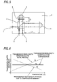
- Fig. 5 is a plan view showing the related-art configuration of a Michelson delay interferometer unit including an optical phase adjusting plate.
- a beam splitter 2, a first reflector 3, a second reflector 4, an input port 5, a first output port 6, and a second output port 7 are mounted in a package 1.
- the package 1 is made of Kovar or the like which has a low coefficient of thermal expansion.
- the distance between the beam splitter 2 and the first reflector 3 is indicated as L1
- the distance between the beam splitter 2 and the second reflector 4 is indicated as L2. Interference is caused by the difference of the distances.
- the optical phase adjusting plate 8 is inserted between the beam splitter 2 and the second reflector 4, and controls the optical path length by the temperature, thereby compensating the optical path variation due to thermal expansion of the package 1 made of Kovar or the like.
- the optical phase adjusting plate 8 may be inserted between the beam splitter 2 and the first reflector 3.
- the temperature independency is realized by placing a compensating member configured by an optical phase adjusting plate 8 made of a thermo-optical effect material which has temperature dependency of the refractive index, in at least one of a portion between the beam splitter 2 and the first reflector 3, and that between the beam splitter 2 and the second reflector 4.
- Fig. 6 is a characteristic graph illustrating the ideal concept of the temperature compensation by an optical phase adjusting plate.
- the optical path length is adjusted by a compensating member having an opposite temperature characteristic F2, thereby realizing the temperature independency characteristic F3.
- Patent References 1 and 2 technically show in detail a logical analysis of compensation in the case where a Si single crystal is used as a material of a high-refractive index medium of the optical phase adjusting plate 8.
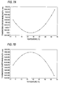
- the temperature compensation by the related-art technique has the following problems.
- Figs. 7A and 7B are actual temperature characteristic diagrams after the temperature compensation which is designed under this assumption. Actually, the temperature characteristic shows a quadratic curve such as shown in Figs. 7A and 7B , and wavelength variation of about 50 pm at 0 to 70°C occurs.
- Exemplary embodiments of the present invention provide a delay interferometer in which an influence on optical components due to temperature variation of a package is suppressed, and a compensation effect owing to an optical phase adjusting plate can be further improved.
- the invention is configured in the following manners.
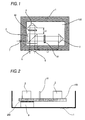
- Fig. 1 is a plan view showing an embodiment of a delay interferometer to which the invention is applied
- Fig. 2 is a side view of the delay interferometer.
- the same components as those of the related-art configuration which has been described with reference to Fig. 5 are denoted by the identical reference numerals, and their description is omitted.
- a first feature of the configuration of the invention is that optical components such as a beam splitter 2, reflectors 3 and 4, and an optical phase adjusting plate 81 or 82 are bonded and fixed onto a low-thermal expansion glass substrate 100.
- a low-thermal expansion glass material which can be employed in the invention, ZERODUR (registered trademark) manufactured by SCHOTT AG, or similar glass having a very low coefficient of thermal expansion (the coefficient of thermal expansion is preferably 0.2 ⁇ 10 -6 /K or less at 0 to 85°C) is useful.
- a second feature of the configuration of the invention is that, as shown in Fig. 2 , the low-thermal expansion glass substrate 100 on which the optical components are mounted is fixed through an elastic member 200 to a supporting member 9 formed on a bottom portion of the package.
- the elastic member of the present invention is an elastic member, which can suppress deformation and stress caused by the thermal expansion coefficient difference due to the difference between a material (for example, Kovar) of the package and a material of the glass substrate on which the optical components are mounted. Further, the elastic member of the present invention is made of a material, which can prevent portions of the elastic member which are bonded to the package and the glass substrate from separating from the package and the glass substrate.
- a third feature of the configuration of the invention is that the optical phase adjusting plates 81, 82 made of the same material (for example, Si) are inserted respectively into the both optical paths L1, 12, thereby offsetting the changes of the refractive indices of the optical phase adjusting plates due to the temperature.
- a thin optical phase adjusting plate which has a thickness of 100 ⁇ m, and which is hardly processed when one of the plates has a thickness of 1,100 ⁇ m and the other plate has a thickness of 1,000 ⁇ m, for example, it is possible to equivalently realize a thin optical phase adjusting plate which has a thickness of 100 ⁇ m. This contributes to cost reduction.
- a thin optical phase adjusting plate which is hardly processed when optical phase adjusting plates which are inserted respectively into optical paths of split optical signals are made different in thickness in the optical axis direction from each other, temperature compensation can be performed based on the thickness difference. Therefore, a thin optical phase adjusting plate can be equivalently realized, thereby contributing to cost reduction.
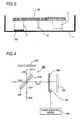
- Fig. 3 is a side view showing another embodiment of a delay interferometer to which the invention is applied.
- the embodiment is characterized in the configuration where the optical components on the low-thermal expansion glass substrate 100 shown in Fig. 2 are placed in an upside down manner, and the block of the beam splitter 2 is directly fixed to the bottom portion of the package 1 through the elastic member 200.
- This configuration exerts the same effects as that of Fig. 2 .
Landscapes
- Physics & Mathematics (AREA)
- General Physics & Mathematics (AREA)
- Optics & Photonics (AREA)
- Optical Communication System (AREA)
- Optical Modulation, Optical Deflection, Nonlinear Optics, Optical Demodulation, Optical Logic Elements (AREA)
- Instruments For Measurement Of Length By Optical Means (AREA)
Applications Claiming Priority (1)
| Application Number | Priority Date | Filing Date | Title |
|---|---|---|---|
| JP2008152240A JP4715872B2 (ja) | 2008-06-10 | 2008-06-10 | 遅延干渉計 |
Publications (2)
| Publication Number | Publication Date |
|---|---|
| EP2133732A2 true EP2133732A2 (de) | 2009-12-16 |
| EP2133732A3 EP2133732A3 (de) | 2010-07-14 |
Family
ID=41010264
Family Applications (1)
| Application Number | Title | Priority Date | Filing Date |
|---|---|---|---|
| EP09162396A Withdrawn EP2133732A3 (de) | 2008-06-10 | 2009-06-10 | Verzögerungs-Interferometer |
Country Status (3)
| Country | Link |
|---|---|
| US (1) | US20090303490A1 (de) |
| EP (1) | EP2133732A3 (de) |
| JP (1) | JP4715872B2 (de) |
Families Citing this family (8)
| Publication number | Priority date | Publication date | Assignee | Title |
|---|---|---|---|---|
| US7799273B2 (en) | 2004-05-06 | 2010-09-21 | Smp Logic Systems Llc | Manufacturing execution system for validation, quality and risk assessment and monitoring of pharmaceutical manufacturing processes |
| US7444197B2 (en) * | 2004-05-06 | 2008-10-28 | Smp Logic Systems Llc | Methods, systems, and software program for validation and monitoring of pharmaceutical manufacturing processes |
| JP4893969B2 (ja) * | 2008-06-10 | 2012-03-07 | 横河電機株式会社 | 遅延干渉計 |
| JP4636449B2 (ja) * | 2008-06-10 | 2011-02-23 | 横河電機株式会社 | 遅延干渉計 |
| JP2012013782A (ja) * | 2010-06-29 | 2012-01-19 | Sumitomo Osaka Cement Co Ltd | 光復調器 |
| JP5779339B2 (ja) * | 2010-11-24 | 2015-09-16 | 日本オクラロ株式会社 | 光モジュール |
| JP2013134320A (ja) * | 2011-12-26 | 2013-07-08 | Fujitsu Telecom Networks Ltd | ラマン増幅用励起光源、ラマン増幅器および光伝送システム |
| US9279658B1 (en) * | 2013-03-14 | 2016-03-08 | Exelis, Inc. | System and method for setting up secondary reflective optic |
Citations (2)
| Publication number | Priority date | Publication date | Assignee | Title |
|---|---|---|---|---|
| JP2007151026A (ja) | 2005-11-30 | 2007-06-14 | Yokogawa Electric Corp | 復調器 |
| JP2007306371A (ja) | 2006-05-12 | 2007-11-22 | Yokogawa Electric Corp | 遅延干渉計及び復調器 |
Family Cites Families (35)
| Publication number | Priority date | Publication date | Assignee | Title |
|---|---|---|---|---|
| DE3334460A1 (de) * | 1983-09-23 | 1985-04-11 | Fa. Carl Zeiss, 7920 Heidenheim | Mehrkoordinaten-messmaschine |
| JPH04216504A (ja) * | 1990-12-17 | 1992-08-06 | Fujitsu Ltd | 光導波路モジュール |
| US5317383A (en) * | 1992-09-18 | 1994-05-31 | Shell Oil Company | Array retroreflector apparatus for remote seismic sensing |
| US5289434A (en) * | 1992-09-18 | 1994-02-22 | Shell Oil Company | Retroreflector apparatus for remote seismic sensing |
| US5327216A (en) * | 1992-09-18 | 1994-07-05 | Shell Oil Company | Apparatus for remote seismic sensing of array signals using side-by-side retroreflectors |
| US5555470A (en) * | 1993-10-12 | 1996-09-10 | The Regents Of The University Of Michigan | Single wave linear interferometric force transducer |
| JP3618450B2 (ja) * | 1995-11-15 | 2005-02-09 | 株式会社ソキア | 多軸レーザ干渉測長機 |
| JP3689949B2 (ja) * | 1995-12-19 | 2005-08-31 | 株式会社ニコン | 投影露光装置、及び該投影露光装置を用いたパターン形成方法 |
| US6330065B1 (en) * | 1997-10-02 | 2001-12-11 | Zygo Corporation | Gas insensitive interferometric apparatus and methods |
| US6141101A (en) * | 1997-11-12 | 2000-10-31 | Plx, Inc. | Monolithic optical assembly |
| US6512588B1 (en) * | 1999-05-05 | 2003-01-28 | Zygo Corporation | Method and system for correcting an interferometric angle measurement for the effects of dispersion |
| US7057741B1 (en) * | 1999-06-18 | 2006-06-06 | Kla-Tencor Corporation | Reduced coherence symmetric grazing incidence differential interferometer |
| US6541759B1 (en) * | 2000-06-20 | 2003-04-01 | Zygo Corporation | Interferometry system having a dynamic beam-steering assembly for measuring angle and distance and employing optical fibers for remote photoelectric detection |
| TWI259898B (en) * | 2002-01-24 | 2006-08-11 | Zygo Corp | Method and apparatus for compensation of time-varying optical properties of gas in interferometry |
| JP2003232957A (ja) * | 2002-02-07 | 2003-08-22 | Furukawa Electric Co Ltd:The | 光モジュール |
| JP4632227B2 (ja) * | 2002-08-15 | 2011-02-16 | Hoya株式会社 | 光モジュール |
| JP2004085966A (ja) * | 2002-08-28 | 2004-03-18 | Hitachi Cable Ltd | 導波路型光モジュール |
| JP4308623B2 (ja) * | 2003-10-27 | 2009-08-05 | 富士通株式会社 | 電気回路を内蔵する光導波路モジュール及びその製造方法 |
| CA2491700A1 (en) * | 2004-12-24 | 2006-06-24 | Dicos Technologies Inc. | High coherence frequency stabilized semiconductor laser |
| US7489874B2 (en) * | 2005-02-28 | 2009-02-10 | Alcatel-Lucent Usa Inc. | Method and apparatus for demodulation of optical differential phase shift keyed signals |
| US7292347B2 (en) * | 2005-08-01 | 2007-11-06 | Mitutoyo Corporation | Dual laser high precision interferometer |
| JP4730772B2 (ja) * | 2005-09-21 | 2011-07-20 | 株式会社フジクラ | フィルタモジュールのパッケージ方法 |
| US7839905B2 (en) * | 2005-12-09 | 2010-11-23 | Massachusetts Institute Of Technology | Carrier-envelope phase shift using linear media |
| DE102006001732A1 (de) * | 2006-01-13 | 2007-07-19 | Robert Bosch Gmbh | Interferometrische Messvorrichtung |
| JP4695989B2 (ja) * | 2006-01-27 | 2011-06-08 | 富士通株式会社 | 差動m位相偏移変調信号の復調用干渉計 |
| KR100781985B1 (ko) * | 2006-07-14 | 2007-12-06 | 삼성전자주식회사 | 변위 간섭계 시스템 및 그가 채용되는 노광설비 |
| WO2008015745A1 (en) * | 2006-08-03 | 2008-02-07 | Nabtesco Corporation | Optical path switching device |
| US7564567B2 (en) * | 2006-09-25 | 2009-07-21 | Massachusetts Institute Of Technology | Sensor for measuring a vibrating surface obscured from view |
| JP2008202959A (ja) * | 2007-02-16 | 2008-09-04 | Sony Corp | 振動検出装置 |
| US8083359B2 (en) * | 2007-11-20 | 2011-12-27 | Mks Instruments, Inc. | Corner cube retroreflector mount |
| JP4636449B2 (ja) * | 2008-06-10 | 2011-02-23 | 横河電機株式会社 | 遅延干渉計 |
| JP4893969B2 (ja) * | 2008-06-10 | 2012-03-07 | 横河電機株式会社 | 遅延干渉計 |
| JP4895052B2 (ja) * | 2008-06-10 | 2012-03-14 | 横河電機株式会社 | 遅延干渉計 |
| JP4461491B2 (ja) * | 2008-06-10 | 2010-05-12 | 横河電機株式会社 | 光学位相調整板 |
| US7995208B2 (en) * | 2008-08-06 | 2011-08-09 | Ftrx Llc | Monolithic interferometer with optics of different material |
-
2008
- 2008-06-10 JP JP2008152240A patent/JP4715872B2/ja not_active Expired - Fee Related
-
2009
- 2009-06-09 US US12/481,161 patent/US20090303490A1/en not_active Abandoned
- 2009-06-10 EP EP09162396A patent/EP2133732A3/de not_active Withdrawn
Patent Citations (2)
| Publication number | Priority date | Publication date | Assignee | Title |
|---|---|---|---|---|
| JP2007151026A (ja) | 2005-11-30 | 2007-06-14 | Yokogawa Electric Corp | 復調器 |
| JP2007306371A (ja) | 2006-05-12 | 2007-11-22 | Yokogawa Electric Corp | 遅延干渉計及び復調器 |
Also Published As
| Publication number | Publication date |
|---|---|
| EP2133732A3 (de) | 2010-07-14 |
| US20090303490A1 (en) | 2009-12-10 |
| JP2009302682A (ja) | 2009-12-24 |
| JP4715872B2 (ja) | 2011-07-06 |
Similar Documents
| Publication | Publication Date | Title |
|---|---|---|
| EP2133732A2 (de) | Verzögerungs-Interferometer | |
| US7585117B2 (en) | Optical module | |
| US6775437B2 (en) | Temperature compensated optical waveguide structures | |
| EP3011647B1 (de) | Wärmeverriegelung | |
| US8456741B2 (en) | Optical module having three or more optically transparent layers | |
| US6829053B1 (en) | Airgap type etalon and apparatus utilizing the same | |
| US7061659B2 (en) | Thermally tuned filter having a pre-stressed membrane | |
| WO2019202632A1 (ja) | 光モジュール | |
| US20170115468A1 (en) | Folding optics for folding an optical path in a laser pulse arrangement | |
| JP3924182B2 (ja) | 可変分散補償器 | |
| GB2393188A (en) | VIPA optical element | |
| US11060913B2 (en) | Tuneable filter | |
| GB2570440A (en) | Optical source and method of assembling an optical source | |
| JP5066494B2 (ja) | 光合分波器 | |
| EP2133657B1 (de) | Optische Phasenänderungsplatte | |
| JP2004109859A (ja) | ミラー固定方法および光学装置 | |
| JP2010011102A (ja) | 遅延干渉計 | |
| US6961498B2 (en) | Coupling device for the alignment of an optical waveguide | |
| JP4473917B2 (ja) | 光信号処理装置 | |
| WO2003032047A1 (en) | Temperature-compensation optical communication interference device and optical communication system | |
| KR100563236B1 (ko) | 광학계의 열팽창 보상 장치 | |
| JP2002236261A (ja) | 可変群遅延ユニット及び可変群遅延モジュール | |
| JPH05157640A (ja) | 光導波路型応力センサ | |
| HK1124180A (en) | Optical module |
Legal Events
| Date | Code | Title | Description |
|---|---|---|---|
| PUAI | Public reference made under article 153(3) epc to a published international application that has entered the european phase |
Free format text: ORIGINAL CODE: 0009012 |
|
| AK | Designated contracting states |
Kind code of ref document: A2 Designated state(s): AT BE BG CH CY CZ DE DK EE ES FI FR GB GR HR HU IE IS IT LI LT LU LV MC MK MT NL NO PL PT RO SE SI SK TR |
|
| PUAL | Search report despatched |
Free format text: ORIGINAL CODE: 0009013 |
|
| AK | Designated contracting states |
Kind code of ref document: A3 Designated state(s): AT BE BG CH CY CZ DE DK EE ES FI FR GB GR HR HU IE IS IT LI LT LU LV MC MK MT NL NO PL PT RO SE SI SK TR |
|
| AX | Request for extension of the european patent |
Extension state: AL BA RS |
|
| RIC1 | Information provided on ipc code assigned before grant |
Ipc: G01B 9/02 20060101ALI20100609BHEP Ipc: G02F 1/00 20060101AFI20091112BHEP |
|
| 17P | Request for examination filed |
Effective date: 20110113 |
|
| STAA | Information on the status of an ep patent application or granted ep patent |
Free format text: STATUS: THE APPLICATION IS DEEMED TO BE WITHDRAWN |
|
| 18D | Application deemed to be withdrawn |
Effective date: 20120103 |