EP2132802B1 - Oled avec couplage de sortie de lumière optimisé - Google Patents
Oled avec couplage de sortie de lumière optimisé Download PDFInfo
- Publication number
- EP2132802B1 EP2132802B1 EP08742456A EP08742456A EP2132802B1 EP 2132802 B1 EP2132802 B1 EP 2132802B1 EP 08742456 A EP08742456 A EP 08742456A EP 08742456 A EP08742456 A EP 08742456A EP 2132802 B1 EP2132802 B1 EP 2132802B1
- Authority
- EP
- European Patent Office
- Prior art keywords
- layer
- low
- index
- electrode
- light
- Prior art date
- Legal status (The legal status is an assumption and is not a legal conclusion. Google has not performed a legal analysis and makes no representation as to the accuracy of the status listed.)
- Active
Links
- 239000000463 material Substances 0.000 claims description 162
- 239000000758 substrate Substances 0.000 claims description 58
- 238000000151 deposition Methods 0.000 claims description 16
- VYPSYNLAJGMNEJ-UHFFFAOYSA-N Silicium dioxide Chemical compound O=[Si]=O VYPSYNLAJGMNEJ-UHFFFAOYSA-N 0.000 claims description 13
- 238000004519 manufacturing process Methods 0.000 claims description 7
- 239000004964 aerogel Substances 0.000 claims description 6
- 239000000377 silicon dioxide Substances 0.000 claims description 6
- 239000004809 Teflon Substances 0.000 claims description 5
- 229920006362 Teflon® Polymers 0.000 claims description 5
- GWEVSGVZZGPLCZ-UHFFFAOYSA-N Titan oxide Chemical compound O=[Ti]=O GWEVSGVZZGPLCZ-UHFFFAOYSA-N 0.000 claims description 4
- 229910052681 coesite Inorganic materials 0.000 claims description 4
- 229910052906 cristobalite Inorganic materials 0.000 claims description 4
- 229910052682 stishovite Inorganic materials 0.000 claims description 4
- 229910052905 tridymite Inorganic materials 0.000 claims description 4
- 239000002073 nanorod Substances 0.000 claims description 2
- 239000010410 layer Substances 0.000 description 169
- 239000012044 organic layer Substances 0.000 description 34
- 239000011521 glass Substances 0.000 description 28
- 230000032258 transport Effects 0.000 description 21
- 239000007924 injection Substances 0.000 description 20
- 238000002347 injection Methods 0.000 description 20
- 150000003384 small molecules Chemical class 0.000 description 19
- 239000011241 protective layer Substances 0.000 description 16
- 230000000903 blocking effect Effects 0.000 description 13
- 230000005525 hole transport Effects 0.000 description 13
- 239000011368 organic material Substances 0.000 description 12
- 238000000034 method Methods 0.000 description 11
- 238000004770 highest occupied molecular orbital Methods 0.000 description 10
- 229910052751 metal Inorganic materials 0.000 description 10
- 239000002184 metal Substances 0.000 description 10
- 229920000642 polymer Polymers 0.000 description 9
- 230000012447 hatching Effects 0.000 description 8
- 238000004768 lowest unoccupied molecular orbital Methods 0.000 description 7
- 239000000243 solution Substances 0.000 description 7
- 150000001875 compounds Chemical class 0.000 description 6
- 239000000412 dendrimer Substances 0.000 description 6
- 229920000736 dendritic polymer Polymers 0.000 description 6
- 239000002019 doping agent Substances 0.000 description 6
- 230000005693 optoelectronics Effects 0.000 description 6
- XCJYREBRNVKWGJ-UHFFFAOYSA-N copper(II) phthalocyanine Chemical compound [Cu+2].C12=CC=CC=C2C(N=C2[N-]C(C3=CC=CC=C32)=N2)=NC1=NC([C]1C=CC=CC1=1)=NC=1N=C1[C]3C=CC=CC3=C2[N-]1 XCJYREBRNVKWGJ-UHFFFAOYSA-N 0.000 description 5
- 238000009826 distribution Methods 0.000 description 5
- 230000008569 process Effects 0.000 description 5
- 239000010405 anode material Substances 0.000 description 4
- 239000002800 charge carrier Substances 0.000 description 4
- -1 e.g. Polymers 0.000 description 4
- 230000000694 effects Effects 0.000 description 4
- 230000007246 mechanism Effects 0.000 description 4
- 229910044991 metal oxide Inorganic materials 0.000 description 4
- 150000004706 metal oxides Chemical class 0.000 description 4
- 239000007787 solid Substances 0.000 description 4
- 125000001424 substituent group Chemical group 0.000 description 4
- 239000012780 transparent material Substances 0.000 description 4
- IXHWGNYCZPISET-UHFFFAOYSA-N 2-[4-(dicyanomethylidene)-2,3,5,6-tetrafluorocyclohexa-2,5-dien-1-ylidene]propanedinitrile Chemical compound FC1=C(F)C(=C(C#N)C#N)C(F)=C(F)C1=C(C#N)C#N IXHWGNYCZPISET-UHFFFAOYSA-N 0.000 description 3
- SCZWJXTUYYSKGF-UHFFFAOYSA-N 5,12-dimethylquinolino[2,3-b]acridine-7,14-dione Chemical compound CN1C2=CC=CC=C2C(=O)C2=C1C=C1C(=O)C3=CC=CC=C3N(C)C1=C2 SCZWJXTUYYSKGF-UHFFFAOYSA-N 0.000 description 3
- 230000007423 decrease Effects 0.000 description 3
- AMGQUBHHOARCQH-UHFFFAOYSA-N indium;oxotin Chemical compound [In].[Sn]=O AMGQUBHHOARCQH-UHFFFAOYSA-N 0.000 description 3
- UEEXRMUCXBPYOV-UHFFFAOYSA-N iridium;2-phenylpyridine Chemical compound [Ir].C1=CC=CC=C1C1=CC=CC=N1.C1=CC=CC=C1C1=CC=CC=N1.C1=CC=CC=C1C1=CC=CC=N1 UEEXRMUCXBPYOV-UHFFFAOYSA-N 0.000 description 3
- 239000000203 mixture Substances 0.000 description 3
- 229910052757 nitrogen Inorganic materials 0.000 description 3
- 230000003287 optical effect Effects 0.000 description 3
- 230000000737 periodic effect Effects 0.000 description 3
- 229920003023 plastic Polymers 0.000 description 3
- 239000004033 plastic Substances 0.000 description 3
- 239000002356 single layer Substances 0.000 description 3
- 238000001228 spectrum Methods 0.000 description 3
- 239000000126 substance Substances 0.000 description 3
- TVIVIEFSHFOWTE-UHFFFAOYSA-K tri(quinolin-8-yloxy)alumane Chemical compound [Al+3].C1=CN=C2C([O-])=CC=CC2=C1.C1=CN=C2C([O-])=CC=CC2=C1.C1=CN=C2C([O-])=CC=CC2=C1 TVIVIEFSHFOWTE-UHFFFAOYSA-K 0.000 description 3
- DHDHJYNTEFLIHY-UHFFFAOYSA-N 4,7-diphenyl-1,10-phenanthroline Chemical group C1=CC=CC=C1C1=CC=NC2=C1C=CC1=C(C=3C=CC=CC=3)C=CN=C21 DHDHJYNTEFLIHY-UHFFFAOYSA-N 0.000 description 2
- DIVZFUBWFAOMCW-UHFFFAOYSA-N 4-n-(3-methylphenyl)-1-n,1-n-bis[4-(n-(3-methylphenyl)anilino)phenyl]-4-n-phenylbenzene-1,4-diamine Chemical group CC1=CC=CC(N(C=2C=CC=CC=2)C=2C=CC(=CC=2)N(C=2C=CC(=CC=2)N(C=2C=CC=CC=2)C=2C=C(C)C=CC=2)C=2C=CC(=CC=2)N(C=2C=CC=CC=2)C=2C=C(C)C=CC=2)=C1 DIVZFUBWFAOMCW-UHFFFAOYSA-N 0.000 description 2
- IJGRMHOSHXDMSA-UHFFFAOYSA-N Atomic nitrogen Chemical compound N#N IJGRMHOSHXDMSA-UHFFFAOYSA-N 0.000 description 2
- LFQSCWFLJHTTHZ-UHFFFAOYSA-N Ethanol Chemical compound CCO LFQSCWFLJHTTHZ-UHFFFAOYSA-N 0.000 description 2
- 229920000144 PEDOT:PSS Polymers 0.000 description 2
- 125000000217 alkyl group Chemical group 0.000 description 2
- 239000010406 cathode material Substances 0.000 description 2
- 230000008859 change Effects 0.000 description 2
- 230000008021 deposition Effects 0.000 description 2
- 238000010586 diagram Methods 0.000 description 2
- JAONJTDQXUSBGG-UHFFFAOYSA-N dialuminum;dizinc;oxygen(2-) Chemical compound [O-2].[O-2].[O-2].[O-2].[O-2].[Al+3].[Al+3].[Zn+2].[Zn+2] JAONJTDQXUSBGG-UHFFFAOYSA-N 0.000 description 2
- 238000000295 emission spectrum Methods 0.000 description 2
- 125000001183 hydrocarbyl group Chemical group 0.000 description 2
- 238000005286 illumination Methods 0.000 description 2
- 239000007788 liquid Substances 0.000 description 2
- 239000011159 matrix material Substances 0.000 description 2
- 150000002739 metals Chemical class 0.000 description 2
- 238000000059 patterning Methods 0.000 description 2
- 229920001467 poly(styrenesulfonates) Polymers 0.000 description 2
- 229960002796 polystyrene sulfonate Drugs 0.000 description 2
- 239000011970 polystyrene sulfonate Substances 0.000 description 2
- 229910052710 silicon Inorganic materials 0.000 description 2
- 239000010703 silicon Substances 0.000 description 2
- 238000010129 solution processing Methods 0.000 description 2
- 238000002207 thermal evaporation Methods 0.000 description 2
- 125000001637 1-naphthyl group Chemical group [H]C1=C([H])C([H])=C2C(*)=C([H])C([H])=C([H])C2=C1[H] 0.000 description 1
- STTGYIUESPWXOW-UHFFFAOYSA-N 2,9-dimethyl-4,7-diphenyl-1,10-phenanthroline Chemical compound C=12C=CC3=C(C=4C=CC=CC=4)C=C(C)N=C3C2=NC(C)=CC=1C1=CC=CC=C1 STTGYIUESPWXOW-UHFFFAOYSA-N 0.000 description 1
- OKTJSMMVPCPJKN-UHFFFAOYSA-N Carbon Chemical compound [C] OKTJSMMVPCPJKN-UHFFFAOYSA-N 0.000 description 1
- 229920001609 Poly(3,4-ethylenedioxythiophene) Polymers 0.000 description 1
- 239000004965 Silica aerogel Substances 0.000 description 1
- XUIMIQQOPSSXEZ-UHFFFAOYSA-N Silicon Chemical compound [Si] XUIMIQQOPSSXEZ-UHFFFAOYSA-N 0.000 description 1
- 239000007983 Tris buffer Substances 0.000 description 1
- 238000010521 absorption reaction Methods 0.000 description 1
- 229910052782 aluminium Inorganic materials 0.000 description 1
- XAGFODPZIPBFFR-UHFFFAOYSA-N aluminium Chemical compound [Al] XAGFODPZIPBFFR-UHFFFAOYSA-N 0.000 description 1
- PNEYBMLMFCGWSK-UHFFFAOYSA-N aluminium oxide Inorganic materials [O-2].[O-2].[O-2].[Al+3].[Al+3] PNEYBMLMFCGWSK-UHFFFAOYSA-N 0.000 description 1
- 125000003118 aryl group Chemical group 0.000 description 1
- 230000004888 barrier function Effects 0.000 description 1
- UHOVQNZJYSORNB-UHFFFAOYSA-N benzene Substances C1=CC=CC=C1 UHOVQNZJYSORNB-UHFFFAOYSA-N 0.000 description 1
- 239000004305 biphenyl Substances 0.000 description 1
- 229910052799 carbon Inorganic materials 0.000 description 1
- 238000006243 chemical reaction Methods 0.000 description 1
- 239000000470 constituent Substances 0.000 description 1
- 229920001577 copolymer Polymers 0.000 description 1
- 238000010168 coupling process Methods 0.000 description 1
- 238000005859 coupling reaction Methods 0.000 description 1
- 230000003247 decreasing effect Effects 0.000 description 1
- 239000006185 dispersion Substances 0.000 description 1
- 239000007772 electrode material Substances 0.000 description 1
- 238000005516 engineering process Methods 0.000 description 1
- 238000000605 extraction Methods 0.000 description 1
- 239000011888 foil Substances 0.000 description 1
- 239000007789 gas Substances 0.000 description 1
- 238000009499 grossing Methods 0.000 description 1
- RBTKNAXYKSUFRK-UHFFFAOYSA-N heliogen blue Chemical compound [Cu].[N-]1C2=C(C=CC=C3)C3=C1N=C([N-]1)C3=CC=CC=C3C1=NC([N-]1)=C(C=CC=C3)C3=C1N=C([N-]1)C3=CC=CC=C3C1=N2 RBTKNAXYKSUFRK-UHFFFAOYSA-N 0.000 description 1
- 239000003446 ligand Substances 0.000 description 1
- 230000000877 morphologic effect Effects 0.000 description 1
- IBHBKWKFFTZAHE-UHFFFAOYSA-N n-[4-[4-(n-naphthalen-1-ylanilino)phenyl]phenyl]-n-phenylnaphthalen-1-amine Chemical compound C1=CC=CC=C1N(C=1C2=CC=CC=C2C=CC=1)C1=CC=C(C=2C=CC(=CC=2)N(C=2C=CC=CC=2)C=2C3=CC=CC=C3C=CC=2)C=C1 IBHBKWKFFTZAHE-UHFFFAOYSA-N 0.000 description 1
- 238000005457 optimization Methods 0.000 description 1
- 238000013086 organic photovoltaic Methods 0.000 description 1
- 230000001151 other effect Effects 0.000 description 1
- 239000002243 precursor Substances 0.000 description 1
- 238000007639 printing Methods 0.000 description 1
- 230000001902 propagating effect Effects 0.000 description 1
- 239000004065 semiconductor Substances 0.000 description 1
- 230000011664 signaling Effects 0.000 description 1
- 235000012239 silicon dioxide Nutrition 0.000 description 1
- 238000003980 solgel method Methods 0.000 description 1
- 238000004528 spin coating Methods 0.000 description 1
- 239000000725 suspension Substances 0.000 description 1
- 230000002195 synergetic effect Effects 0.000 description 1
- ODHXBMXNKOYIBV-UHFFFAOYSA-N triphenylamine Chemical compound C1=CC=CC=C1N(C=1C=CC=CC=1)C1=CC=CC=C1 ODHXBMXNKOYIBV-UHFFFAOYSA-N 0.000 description 1
- 238000001947 vapour-phase growth Methods 0.000 description 1
- 239000003981 vehicle Substances 0.000 description 1
- 238000003466 welding Methods 0.000 description 1
- 238000009736 wetting Methods 0.000 description 1
- YVTHLONGBIQYBO-UHFFFAOYSA-N zinc indium(3+) oxygen(2-) Chemical compound [O--].[Zn++].[In+3] YVTHLONGBIQYBO-UHFFFAOYSA-N 0.000 description 1
Images


Classifications
-
- H—ELECTRICITY
- H10—SEMICONDUCTOR DEVICES; ELECTRIC SOLID-STATE DEVICES NOT OTHERWISE PROVIDED FOR
- H10K—ORGANIC ELECTRIC SOLID-STATE DEVICES
- H10K50/00—Organic light-emitting devices
- H10K50/80—Constructional details
- H10K50/85—Arrangements for extracting light from the devices
- H10K50/858—Arrangements for extracting light from the devices comprising refractive means, e.g. lenses
Definitions
- the present invention relates to organic light emitting devices (OLEDs), and more specifically to organic light emitting devices having a low refractive-index material that enhances light outcoupling.
- Opto-electronic devices that make use of organic materials are becoming increasingly desirable for a number of reasons. Many of the materials used to make such devices are relatively inexpensive, so organic opto-electronic devices have the potential for cost advantages over inorganic devices. In addition, the inherent properties of organic materials, such as their flexibility, may make them well suited for particular applications such as fabrication on a flexible substrate. Examples of organic opto-electronic devices include organic light emitting devices (OLEDs), organic phototransistors, organic photovoltaic cells, and organic photodetectors. For OLEDs, the organic materials may have performance advantages over conventional materials. For example, the wavelength at which an organic emissive layer emits light may generally be readily tuned with appropriate dopants.
- OLEDs organic light emitting devices
- the wavelength at which an organic emissive layer emits light may generally be readily tuned with appropriate dopants.
- organic includes polymeric materials as well as small molecule organic materials that may be used to fabricate organic opto-electronic devices.
- Small molecule refers to any organic material that is not a polymer, and "small molecules” may actually be quite large. Small molecules may include repeat units in some circumstances. For example, using a long chain alkyl group as a substituent does not remove a molecule from the "small molecule” class. Small molecules may also be incorporated into polymers, for example as a pendent group on a polymer backbone or as a part of the backbone. Small molecules may also serve as the core moiety of a dendrimer, which consists of a series of chemical shells built on the core moiety.
- the core moiety of a dendrimer may be a fluorescent or phosphorescent small molecule emitter.
- a dendrimer may be a "small molecule," and it is believed that all dendrimers currently used in the field of OLEDs are small molecules.
- a small molecule has a well-defined chemical formula with a single molecular weight, whereas a polymer has a chemical formula and a molecular weight that may vary from molecule to molecule.
- organic includes metal complexes of hydrocarbyl and heteroatom-substituted hydrocarbyl ligands.
- OLEDs make use of thin organic films that emit light when voltage is applied across the device. OLEDs are becoming an increasingly interesting technology for use in applications such as flat panel displays, illumination, and backlighting. Several OLED materials and configurations are described in U.S. Patent Nos. 5,844,363 , 6,303,238 , and 5,707,745 .
- OLED devices are generally (but not always) intended to emit light through at least one of the electrodes, and one or more transparent electrodes may be useful in an organic opto-electronic devices.
- a transparent electrode material such as indium tin oxide (ITO)
- ITO indium tin oxide
- a transparent top electrode such as disclosed in U.S. Patent Nos. 5,703,436 and 5,707,745 , may also be used.
- the top electrode does not need to be transparent, and may be comprised of a thick and reflective metal layer having a high electrical conductivity.
- the bottom electrode may be opaque and / or reflective.
- an electrode does not need to be transparent, using a thicker layer may provide better conductivity, and using a reflective electrode may increase the amount of light emitted through the other electrode, by reflecting light back towards the transparent electrode.
- Fully transparent devices may also be fabricated, where both electrodes are transparent.
- Side emitting OLEDs may also be fabricated, and one or both electrodes may be opaque or reflective in such devices.
- top means furthest away from the substrate
- bottom means closest to the substrate.
- the bottom electrode is the electrode closest to the substrate, and is generally the first electrode fabricated.
- the bottom electrode has two surfaces, a bottom surface closest to the substrate, and a top surface further away from the substrate.
- a first layer is described as "disposed over” a second layer
- the first layer is disposed further away from substrate.
- a cathode may be described as “disposed over” an anode, even though there are various organic layers in between.
- solution processible means capable of being dissolved, dispersed, or transported in and/or deposited from a liquid medium, either in solution or suspension form.
- a first "Highest Occupied Molecular Orbital” (HOMO) or “Lowest Unoccupied Molecular Orbital” (LUMO) energy level is "greater than” or "higher that" a second HOMO or LUMO energy level if the first energy level is closer to the vacuum energy level. Since ionization potentials (IP) are measured as a negative energy relative to a vacuum level, a higher HOMO energy level corresponds to an IP having a smaller absolute value (an IP that is less negative). Similarly, a higher LUMO energy level corresponds to an electron affinity (EA) having a smaller absolute value (an EA that is less negative).
- IP ionization potentials
- EA electron affinity
- US 2004/0160165 A1 discloses a display panel including a light-emitting layer, a protective layer, a reflective layer, and a reflective surface.
- the protective layer is deposited on an emitting side of the light emitting layer and forms an interface with an external medium.
- the protective layer has a thickness that allows the light emitted from the light-emitting layer to undergo total reflection at least once at the interface in an area of the light-emitting layer.
- the reflective layer is deposited on an opposite side of the protective layer with respect to the light-emitting layer.
- the reflective surface is at a periphery of the light-emitting layer and changes the direction of the light propagating inside the protective layer emitted from the light-emitting layer.
- the invention is directed to a device comprising a substrate, a first electrode disposed over the substrate and an organic payer disposed over the first electrode, the organic layer comprising a first region comprising an organic emissive material and a second region comprising periods of a transparent low-index material embedded within the organic layer, wherein the low-index material has a refractive index less than the refractive index of the organic emissive material, wherein the device further comprises a second electrode disposed over the organic layer, wherein the periods of the transparent low-index material embedded within the organic layer provide an enhanced outcoupling efficiency over a broad spectrum with substantially no distortion of the emission spectrum of the extracted light, and wherein at least one of the first and second electrodes is a transparent electrode.
- the invention is also directed to a method of manufacturing a light-emitting device, comprising depositing a first electrode over a substrate, depositing a grid of a low-index material having a refractive index of 1.0 to 1.5 over the first electrode, depositing an organic emissive material over the grid such that the organic emissive material is in direct contact with the grid or with the first electrode and depositing a second electrode over the organic emissive material, wherein at least one of the first and second electrodes is a transparent electrode and wherein the grid of the low-index material redirects light emitted hy the organic emissive material from a waveguide mode to a direction that may escape the device through the transparent electrode.
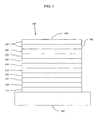
- FIG. 1 shows an organic light emitting device having separate electron transport, hole transport, and emissive layers, as well as other layers.
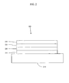
- FIG. 2 shows an inverted organic light emitting device that does not have a separate electron transport layer.
- FIG. 3A shows an organic light emitting device having regions of a transparent material with a low refractive index.
- FIG. 3B shows a portion of a device where the boundary between adjacent regions is roughly perpendicular.
- FIG. 3C shows a portion of a device where the boundary between adjacent regions is rough.
- FIG. 3D shows an organic light emitting device having regions of a transparent material with a low refractive index.
- FIGS. 4A and 4B show top views of exemplary configurations of a low-index region.
- FIG. 5A shows simulated values for the amount of light converted to air mode and glass mode for a device having a low-index region.
- FIG. 5B shows simulated emission for a device having a hexagonal grid of a low-index material having a refractive index of 1.03.
- FIG. 6A shows a device having a microlens sheet.
- FIG. 6B shows a device having a thin low-index layer disposed between the substrate and an electrode.
- FIG. 7 shows the proportion of light emitted by a device with a microlens, having a hexagonal grid of low-index material for a range of refractive indices.
- FIG. 8 shows the proportion of light emitted for a conventional OLED, an OLED with an ideal microlens, and an OLED with an ideal microlens and a hexagonal grid of a low-index material with a refractive index of 1.29.
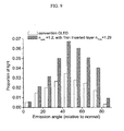
- FIG. 9 shows the light emitted by a conventional OLED and by an OLED with a hexagonal grid of a low-index material having a refractive index of 1.2 and an inserted layer of Teflon AF having a refractive index of 1.29.
- FIG. 10 shows the emission for a device having the same structure as FIG. 9 , but with the low-index material having a refractive index of 1.29.
- FIG. 11 shows the angular distribution of light in a glass substrate without a low-index layer.
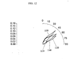
- FIG. 12 shows the angular distribution of light in a glass substrate with a low-index layer.
- FIG. 13 shows the proportion of emitted light as a function of the emission angle for various device structures.
- FIG. 14 shows the proportion of light in air mode and glass mode in devices with various electrode thicknesses.
- FIG. 15 shows the proportion of light in various modes for device having low-index regions of varying width.
- FIG. 16 shows the proportion of light in various modes for a device having organic regions from 4 ⁇ m to 10 ⁇ m.
- FIG. 17 shows the proportion of light in various modes for a device having low-index regions with varying refractive indices and geometries.
- FIG. 18 shows a transparent or top emitting organic light emitting device having regions of a transparent material with a low refractive index.
- FIGS. 19A-19C show a transparent or top emitting OLED with a LIG embedded in the organic layer.
- FIG. 20A-20C show simulated values for the enhancement in outcoupling efficiency for a transparent or top emitting OLED with a rectangular LIG.
- FIG. 21 shows a transparent or top emitting OLED having a microlens sheet.
- an OLED comprises at least one organic layer disposed between and electrically connected to an anode and a cathode.
- the anode injects holes and the cathode injects electrons into the organic layer(s).
- the injected holes and electrons each migrate toward the oppositely charged electrode.
- an "exciton” which is a localized electron-hole pair having an excited energy state, is formed.
- Light is emitted when the exciton relaxes via a photoemissive mechanism.
- the exciton may be localized on an excimer or an exciplex. Non-radiative mechanisms, such as thermal relaxation, may also occur, but are generally considered undesirable.
- Fig. 1 shows an organic light emitting device 100.
- Device 100 may include a substrate 110, an anode 115, a hole injection layer 120, a hole transport layer 125, an electron blocking layer 130, an emissive layer 135, a hole blocking layer 140, an electron transport layer 145, an electron injection layer 150, a protective layer 155, and a cathode 160.
- Cathode 160 is a compound cathode having a first conductive layer 162 and a second conductive layer 164.
- Device 100 may be fabricated by depositing the layers described, in order.
- Substrate 110 may be any suitable substrate that provides desired structural properties.
- Substrate 110 may be flexible or rigid.
- Substrate 110 may be transparent, translucent or opaque.
- Plastic and glass are examples of preferred rigid substrate materials.
- Plastic and metal foils are examples of preferred flexible substrate materials.
- Substrate 110 may be a semiconductor material in order to facilitate the fabrication of circuitry.
- substrate 110 may be a silicon wafer upon which circuits are fabricated, capable of controlling OLEDs subsequently deposited on the substrate: Other substrates may be used.
- the material and thickness of substrate 110 may be chosen to obtain desired structural and optical properties.
- Anode 115 may be any suitable anode that is sufficiently conductive to transport holes to the organic layers.
- the material of anode 115 preferably has a work function higher than about 4 eV (a "high work function material").
- Preferred anode materials include conductive metal oxides, such as indium tin oxide (ITO) and indium zinc oxide (IZO), aluminum zinc oxide (AlZnO), and metals.
- Anode 115 (and substrate 110) may be sufficiently transparent to create a bottom-emitting device.
- a preferred transparent substrate and anode combination is commercially available ITO (anode) deposited on glass or plastic (substrate).
- a flexible and transparent substrate-anode combination is disclosed in United States Patent Nos.
- Anode 115 may be opaque and / or reflective. A reflective anode 115 may be preferred for some top-emitting devices, to increase the amount of light emitted from the top of the device.
- the material and thickness of anode 115 may be chosen to obtain desired conductive and optical properties. Where anode 115 is transparent, there may be a range of thickness for a particular material that is thick enough to provide the desired conductivity, yet thin enough to provide the desired degree of transparency. Other anode materials and structures may be used.
- Hole transport layer 125 may include a material capable of transporting holes.
- Hole transport layer 130 may be intrinsic (undoped), or doped. Doping may be used to enhance conductivity.
- ⁇ -NPD and TPD are examples of intrinsic hole transport layers.
- An example of a p-doped hole transport layer is m-MTDATA doped with F 4 -TCNQ at a molar ratio of 50:1, as disclosed in United States Patent Application Publication No. 2003-0230980 to Forrest et al. Other hole transport layers may be used.
- Emissive layer 135 may include an organic material capable of emitting light when a current is passed between anode 115 and cathode 160.
- emissive layer 135 contains a phosphorescent emissive material, although fluorescent emissive materials may also be used. Phosphorescent materials are preferred because of the higher luminescent efficiencies associated with such materials.
- Emissive layer 135 may also comprise a host material capable of transporting electrons and / or holes, doped with an emissive material that may trap electrons, holes, and / or excitons, such that excitons relax from the emissive material via a photoemissive mechanism.
- Emissive layer 135 may comprise a single material that combines transport and emissive properties.
- emissive layer 135 may comprise other materials, such as dopants that tune the emission of the emissive material.
- Emissive layer 135 may include a plurality of emissive materials capable of, in combination, emitting a desired spectrum of light. Examples of phosphorescent emissive materials include Ir(ppy) 3 . Examples of fluorescent emissive materials include DCM and DMQA. Examples of host materials include Alq 3 , CBP and mCP. Examples of emissive and host materials are disclosed in U.S. Patent No. 6,303,238 to Thompson et al. Emissive material may be included in emissive layer 135 in a number of ways.
- an emissive small molecule may be incorporated into a polymer. This may be accomplished by several ways: by doping the small molecule into the polymer either as a separate and distinct molecular species; or by incorporating the small molecule into the backbone of the polymer, so as to form a co-polymer; or by bonding the small molecule as a pendant group on the polymer.
- Other emissive layer materials and structures may be used.
- a small molecule emissive material may be present as the core of a dendrimer.
- Electron transport layer 145 may include a material capable of transporting electrons. Electron transport layer 145 may be intrinsic (undoped), or doped. Doping may be used to enhance conductivity. Alq 3 is an example of an intrinsic electron transport layer. An example of an n-doped electron transport layer is BPhen doped with Li at a molar ratio of 1:1, as disclosed in United States Patent Application Publication No. 2003-02309890 to Forrest et al. . Other electron transport layers may be used.
- Cathode 160 may be any suitable material or combination of materials known to the art, such that cathode 160 is capable of conducting electrons and injecting them into the organic layers of device 100. Cathode 160 may be transparent or opaque, and may be reflective. Metals and metal oxides are examples of suitable cathode materials. Cathode 160 may be a single layer, or may have a compound structure. Figure 1 shows a compound cathode 160 having a thin metal layer 162 and a thicker conductive metal oxide layer 164. In a compound cathode, preferred materials for the thicker layer 164 include ITO, IZO, and other materials known to the art. U.S. Patent Nos.
- cathodes including compound cathodes having a thin layer of metal such as Mg:Ag with an overlying transparent, electrically-conductive, sputter-deposited ITO layer.
- the part of cathode 160 that is in contact with the underlying organic layer, whether it is a single layer cathode 160, the thin metal layer 162 of a compound cathode, or some other part, is preferably made of a material having a work function lower than about 4 eV (a "low work function material").
- Other cathode materials and structures may be used.
- Blocking layers may be used to reduce the number of charge carriers (electrons or holes) and / or excitons that leave the emissive layer.
- An electron blocking layer 130 may be disposed between emissive layer 135 and the hole transport layer 125, to block electrons from leaving emissive layer 135 in the direction of hole transport layer 125.
- a hole blocking layer 140 may be disposed between emissive layer135 and electron transport layer 145, to block holes from leaving emissive layer 135 in the direction of electron transport layer 145.
- Blocking layers may also be used to block excitons from diffusing out of the emissive layer. The theory and use of blocking layers is described in more detail in United States Patent No. 6,097,147 and United States Patent Application Publication No. 2003-02309890 to Forrest et al.
- blocking layer means that the layer provides a barrier that significantly inhibits transport of charge carriers and/or excitons through the device, without suggesting that the layer necessarily completely blocks the charge carriers and/or excitons.
- the presence of such a blocking layer in a device may result in substantially higher efficiencies as compared to a similar device lacking a blocking layer.
- a blocking layer may be used to confine emission to a desired region of an OLED.
- injection layers are comprised of a material that may improve the injection of charge carriers from one layer, such as an electrode or an organic layer, into an adjacent organic layer. Injection layers may also perform a charge transport function.
- hole injection layer 120 may be any layer that improves the injection of holes from anode 115 into hole transport layer 125.
- CuPc is an example of a material that may be used as a hole injection layer from an ITO anode 115, and other anodes.
- electron injection layer 150 may be any layer that improves the injection of electrons into electron transport layer 145.
- LiF / Al is an example of a material that may be used as an electron injection layer into an electron transport layer from an adjacent layer. Other materials or combinations of materials may be used for injection layers.
- injection layers may be disposed at locations different than those shown in device 100. More examples of injection layers are provided in U.S. Patent Application Serial No. 09/931,948 to Lu et al. .
- a hole injection layer may comprise a solution deposited material, such as a spin-coated polymer, e.g., PEDOT:PSS, or it may be a vapor deposited small molecule material, e.g., CuPc or MTDATA.
- a hole injection layer may planarize or wet the anode surface so as to provide efficient hole injection from the anode into the hole injecting material.
- a hole injection layer may also have a charge carrying component having HOMO (Highest Occupied Molecular Orbital) energy levels that favorably match up, as defined by their herein-described relative ionization potential (IP) energies, with the adjacent anode layer on one side of the HIL and the hole transporting layer on the opposite side of the HIL.
- the "charge carrying component” is the material responsible for the HOMO energy level that actually transports holes. This component may be the base material of the HIL, or it may be a dopant.
- a doped HIL allows the dopant to be selected for its electrical properties, and the host to be selected for morphological properties such as wetting, flexibility, toughness, etc.
- Preferred properties for the HIL material are such that holes can be efficiently injected from the anode into the HIL material.
- the charge carrying component of the HIL preferably has an IP not more than about 0.7 eV greater that the IP of the anode material. More preferably, the charge carrying component has an IP not more than about 0.5 eV greater than the anode material. Similar considerations apply to any layer into which holes are being injected.
- HIL materials are further distinguished from conventional hole transporting materials that are typically used in the hole transporting layer of an OLED in that such HIL materials may have a hole conductivity that is substantially less than the hole conductivity of conventional hole transporting materials.
- the thickness of the HIL of the present invention may be thick enough to help planarize or wet the surface of the anode layer. For example, an HIL thickness of as little as 10 nm may be acceptable for a very smooth anode surface. However, since anode surfaces tend to be very rough, a thickness for the HIL of up to 50 nm may be desired in some cases.
- a protective layer may be used to protect underlying layers during subsequent fabrication processes.
- the processes used to fabricate metal or metal oxide top electrodes may damage organic layers, and a protective layer may be used to reduce or eliminate such damage.
- protective layer 155 may reduce damage to underlying organic layers during the fabrication of cathode 160.
- a protective layer has a high carrier mobility for the type of carrier that it transports (electrons in device 100), such that it does not significantly increase the operating voltage of device 100.
- CuPc, BCP, and various metal phthalocyanines are examples of materials that may be used in protective layers. Other materials or combinations of materials may be used.
- protective layer 155 is preferably thick enough that there is little or no damage to underlying layers due to fabrication processes that occur after organic protective layer 160 is deposited, yet not so thick as to significantly increase the operating voltage of device 100.
- Protective layer 155 may be doped to increase its conductivity.
- a CuPc or BCP protective layer 160 may be doped with Li.
- Figure 2 shows an inverted OLED 200.
- the device includes a substrate 210, an cathode 215, an emissive layer 220, a hole transport layer 225, and an anode 230.
- Device 200 may be fabricated by depositing the layers described, in order. Because the most common OLED configuration has a cathode disposed over the anode, and device 200 has cathode 215 disposed under anode 230, device 200 may be referred to as an "inverted" OLED. Materials similar to those described with respect to device 100 may be used in the corresponding layers of device 200. Figure 2 provides one example of how some layers may be omitted from the structure of device 100.
- the simple layered structure illustrated in Figures 1 and 2 is provided by way of non-limiting example, and it is understood that embodiments of the invention may be used in connection with a wide variety of other structures.
- the specific materials and structures described are exemplary in nature, and other materials and structures may be used.
- Functional OLEDs may be achieved by combining the various layers described in different ways, or layers may be omitted entirely, based on design, performance, and cost factors. Other layers not specifically described may also be included. Materials other than those specifically described may be used. Although many of the examples provided herein describe various layers as comprising a single material, it is understood that combinations of materials, such as a mixture of host and dopant, or more generally a mixture, may be used. Also, the layers may have various sublayers.
- hole transport layer 225 transports holes and injects holes into emissive layer 220, and may be described as a hole transport layer or a hole injection layer.
- an OLED may be described as having an "organic layer" disposed between a cathode and an anode. This organic layer may comprise a single layer, or may further comprise multiple layers of different organic materials as described, for example, with respect to Figures 1 and 2 .
- OLEDs comprised of polymeric materials (PLEDs) such as disclosed in U.S. Pat. No. 5,247,190, Friend et al.
- PLEDs polymeric materials
- OLEDs having a single organic layer may be used.
- OLEDs may be stacked, for example as described in U.S. Patent No. 5,707,745 to Forrest et al , which is incorporated by reference in its entirety.
- the OLED structure may deviate from the simple layered structure illustrated in Figures 1 and 2 .
- the substrate may include an angled reflective surface to improve out-coupling, such as a mesa structure as described in U.S. Patent No. 6,091,195 to Forrest et al. , and / or a pit structure as described in U.S. Patent No. 5,834,893 to Bulovic et al. .
- any of the layers of the various embodiments may be deposited by any suitable method.
- preferred methods include thermal evaporation, ink-jet, such as described in U.S. Patent Nos. 6,013,982 and 6,087,196 organic vapor phase deposition (OVPD), such as described in U.S. Patent No. 6,337,102 to Forrest et al. , and deposition by organic vapor jet printing (OVJP), such as described in U.S. Patent Application No. 10/233,470 .
- OVPD organic vapor phase deposition
- OJP organic vapor jet printing
- Other suitable deposition methods include spin coating and other solution based processes. Solution based processes are preferably carried out in nitrogen or an inert atmosphere.
- preferred methods include thermal evaporation.
- Preferred patterning methods include deposition through a mask, cold welding such as described in U.S. Patent Nos. 6,294,398 and 6,468,819 , and patterning associated with some of the deposition methods such as ink-jet and OVJP. Other methods may also be used.
- the materials to be deposited may be modified to make them compatible with a particular deposition method.
- substituents such as alkyl and aryl groups, branched or unbranched, and preferably containing at least 3 carbons, may be used in small molecules to enhance their ability to undergo solution processing. Substituents having 20 carbons or more may be used, and 3-20 carbons is a preferred range. Materials with asymmetric structures may have better solution processibility than those having symmetric structures, because asymmetric materials may have a lower tendency to recrystallize. Dendrimer substituents may be used to enhance the ability of small molecules to undergo solution processing.
- Devices fabricated in accordance with embodiments of the invention may be incorporated into a wide variety of consumer products, including flat panel displays, computer monitors, televisions, billboards, lights for interior or exterior illumination and / or signaling, heads up displays, fully transparent displays, flexible displays, laser printers, telephones, cell phones, personal digital assistants (PDAs), laptop computers, digital cameras, camcorders, viewfinders, micro-displays, vehicles, a large area wall, theater or stadium screen, or a sign.
- PDAs personal digital assistants
- Various control mechanisms may be used to control devices fabricated in accordance with the present invention, including passive matrix and active matrix. Many of the devices are intended for use in a temperature range comfortable to humans, such as 18 degrees C to 30 degrees C, and more preferably at room temperature (20 - 25 degrees C).
- the materials and structures described herein may have applications in devices other than OLEDs.
- other optoelectronic devices such as organic solar cells and organic photodetectors may employ the materials and structures.
- organic devices such as organic transistors, may employ the materials and structures.
- a large portion of light originating in an emissive layer within an OLED does not escape the device due to internal reflection at the air interface, edge emission, dissipation within the emissive or other layers, waveguide effects within the emissive layer or other layers of the device (i.e., transporting layers, injection layers, etc.), and other effects.
- Light generated and/or emitted by an OLED may be described as being in various modes, such as "air mode” (the light will be emitted from a viewing surface of the device, such as through the substrate) or "waveguide mode" (the light is trapped within the device due to waveguide effects).
- regions of a transparent material having a low refractive index may be placed adjacent to regions containing an emissive material, in a direction parallel to one or both of the OLED electrodes. These regions may cause light emitted by the emissive material to enter a glass mode or air mode, increasing the proportion of emitted light that ultimately leaves the device.
- top and transparent emitting OLEDs may be enhanced by 2 to 3 times by embedding periods of low index material in these devices without distorting the viewing spectra.
- a transparent emitting OLED refers to an OLED having substantially transparent top and bottom electrodes.
- a top emitting OLED refers to an OLED intended to emit light only through the top (transparent) electrode.
- FIG. 3A shows a side schematic view of an exemplary device 300 having low-index regions 310.
- the device includes a substrate 304, electrodes 301 and 303, and a layer 302 that has regions of one or more emissive materials 305 and regions of a transparent low-index material 310. It will be understood that the device shown in FIG. 3A may also include the various other layers and structures described herein.
- the low-index material preferably contains a material that has a refractive index that is less than the refractive index of the substrate, and more preferably that is 0.15 to 0.4 less than the refractive index of the substrate, as this may increase the amount of waveguide mode light that is converted to air mode and/or glass mode. It may be preferred for the low-index material to have a refractive index of 1.0 to 1.3, and more preferably 1.0 to 1.05. Often the low-index material will have a refractive index lower than the refractive index of the organic materials used in the device, since organic materials used in OLEDs typically have a refractive index of about 1.5-1.7.
- Various low-index materials may be used for the low-index region, such as Teflon, aerogels, graded films of SiO 2 and TiO 2 , and layers of SiO 2 nanorods.
- Various aerogels are known in the art, such as silica, carbon, alumina, and other aerogels.
- a silica aerogel can be made by mixing a liquid alcohol with a silicon alkoxide precursor to form a silicon dioxide sol gel. The alcohol is then removed from the gel and replaced with a gas using various techniques known in the art.
- An aerogel prepared using a sol-gel method may be preferred in some configurations, since the refractive index can be controlled by changing the ratios of the starting solutions. It is also preferred that the low-index material be transparent.
- a material is "transparent" if, at the scale and dimension described for the low-index layers and regions, the total optical loss for light passing through the low-index layer or region in a direction roughly parallel to the electrodes is less than about 50%.
- the low-index material may also be a non-emissive material.
- FIG. 3A shows exemplary rays 320, 330, 340 to indicate various possible outcomes when light is emitted by emissive material in the OLED.
- some light 330 produced by the emissive material may directly exit the device, the light 320 produced in a waveguide mode would typically be unable to exit the emissive layer.
- such light 320 may be modeled as traveling within the emissive layer at a sufficiently large angle relative to the electrode normal that it will never be incident on the emissive layer interface.
- waveguide mode light 340 may be modeled as a ray that is incident on the emissive layer interface, but at a sufficiently high angle ⁇ to undergo total internal reflection. Such light would normally not be emitted from either the top or bottom of the device 300, but may be emitted from a side surface.
- low-index regions next to the emissive regions may allow light that would not normally be emitted by the device, or that would only be emitted from a side of the device, to exit through a viewing surface of the device. As shown in FIG. 3A , light entering the low-index regions is refracted, allowing it to exit the device directly (320) or after reflecting off an electrode (340). That is, light passing through the low-index regions may be converted from waveguide mode to air mode, allowing it to be emitted from the device.
- FIG. 3A shows the boundaries between low-index regions 310 and adjacent organic regions 305 as being flat interfaces perpendicular to the electrodes and substrate, this may not always be the case.
- various deposition methods may be used for the low-index regions and/or the organic regions that result in rough boundaries, or boundaries that are not perpendicular to the substrate.
- FIG. 3B shows an example of a portion of a device where the boundary between a low-index region 310 and an adjacent organic region 305 is not precisely perpendicular to the electrodes 301, 303.
- a specific configuration is illustrated, it will be understood that the regions may have various different cross-sections from those shown.
- the boundary between adjacent regions 305, 310 is roughly perpendicular to an electrode of the device.
- the boundary between two adjacent regions is “roughly perpendicular" to a surface if the angle between the boundary and a plane normal to the surface is 20° or less.
- the boundary between regions 305 and 310 is roughly perpendicular to the electrode 303 when the illustrated angle 350 is 20° or less.
- the boundary between adjacent regions also may be rough, as illustrated in FIG. 3C . In such a configuration, the regions are "roughly perpendicular" to a surface if the angle between a best-fit plane 355 and a plane normal to the surface of the device is 20° or less.
- the boundary between the regions 305, 310 shown in FIG. 3C is roughly perpendicular to the electrode 303 when the angle between the best-fit plane 355 and a plane normal to the electrode 303 is 20° or less.
- the low-index region(s) may extend partially between the electrodes and/or other layers, as shown in FIG. 3D .
- a low-index material 310 may be deposited on an electrode 303.
- the low-index material may be deposited in the various patterns, grids, and other structures as previously described.
- One or more organic materials 305 may then be deposited over the electrode 303 and the low-index regions 310, resulting in an organic layer with an uneven surface.
- An electrode 301 or other layer may be deposited on the organic layer 305, such that the resulting surface is also uneven, or the electrode 301 or other layer may be deposited so as to create a smooth surface.
- a smoothing layer 360 or other layer may also be deposited to create an even surface.
- the low-index region may be arranged in various configurations within the device. It may be preferred for the low-index material to be arranged in a grid. As used herein, a "grid" refers to a repeating pattern of the material.
- FIGS. 4A-4B show exemplary arrangements of the low-index material and regions for use within a device.
- FIG. 4A shows a top view of a low-index material 410 arranged in a hexagonal grid.
- FIG. 4B shows a top view of a low-index material 410 arranged in a rectangular grid.
- the structures shown in FIGS. 4A-4B may be placed within an OLED in a plane parallel to one or both of the electrodes. Such a device may then have a cross-section equivalent to the device illustrated in FIG.
- Emissive regions 420 can include emissive material, charge transport and/or blocking materials, and the other structures and layers described herein. Although it may be preferred for each repeated portion of the grid to have approximately the same dimensions, portions of the grid may have varying dimensions. For a regular pattern, i.e., one where regions of emissive material are surrounded by low-index regions each having the same dimension, the grid may be characterized by a width 421. For example, a regular rectangular grid has emissive regions that are square when viewed from above. Other grid types, such as triangular or octagonal, also may be used, as well as various other patterns and structures.
- the specific shape of the grid may be selected based on desired qualities of the resulting device.
- FIG. 5A shows simulated values for the amount of light that is converted to air mode and glass mode for a device having low-index material in arranged in the grids shown in FIGS. 4A and 4B for a range of refractive indices.
- the data is simulated for a device having organic emissive regions about 5 ⁇ m wide, low-index regions about 0.8 ⁇ m wide, and a top ITO electrode 100 nm thick.
- the amount of light ultimately converted to air mode in a device having a square grid (vertical hashing) and a hexagonal grid (solid), and to glass mode in a device having a square grid (horizontal hatching) and a hexagonal grid (diagonal hatching) is shown.
- the levels approach those for a conventional OLED, i.e., one without low-index regions, when the low-index region is modeled as having a refractive index around 1.7 - 1.8 (510). This is expected, since organic materials typically used in OLEDs can have refractive indices of about 1.7 - 1.8.
- FIG. 5B shows simulated emission for a device having a hexagonal grid of a low-index material having a refractive index of 1.03.
- the width of the emissive regions is 5 ⁇ m
- the width of the low-index regions is 0.8 ⁇ m
- the electrode is a 100 nm ITO layer.
- the outcoupling efficiency of the device may increase to 0.44, as shown.
- An OLED with an ideal microlens disposed on the viewing surface (cross-hatching) generally has an outcoupling efficiency of about 0.32, while the measured value for such a device is generally about 0.26.
- the outcoupling efficiency of the modeled device is about 0.17.
- the low-index region may have a synergistic effect with configurations that enhance conversion from glass mode to air mode.
- the low-index region may convert light from an organic mode to a glass mode, and the glass mode light may be converted to air mode due to the substrate configuration or composition.
- a microlens sheet 610 as shown in FIG.
- the substrate may include a microlens or microlens sheet. Other configurations may be used, such as a centimeter-scale hemispherical glass lens, or a substrate having a roughened surface at the substrate-air interface.
- the substrate may also include different materials, such as materials having different indices of refraction; this can also increase the amount of glass mode light converted to air mode.
- a thin layer 620 of a low-index material such as aerogel or Teflon may also be disposed between the substrate 304 and the electrode 303. This layer may also direct more otherwise glass mode light into an electrode or organic mode, where it will eventually enter a low-index region and become glass mode light.
- FIGS. 7 and 8 show the calculated proportion of light emitted by a device having the same basic structure as the device of FIG. 5B as a function of the viewing angle.
- FIG. 7 shows the proportion of light emitted by a device with a microlens, having a hexagonal grid of low-index material with a refractive index of 1.03 (cross-hatching), 1.2 (no hatching), and 1.29 (solid). As illustrated, the outcoupling efficiency of the device may be as high as 0.60.
- FIG. 7 shows the proportion of light emitted by a device with a microlens, having a hexagonal grid of low-index material with a refractive index of 1.03 (cross-hatching), 1.2 (no hatching), and 1.29 (solid).
- the outcoupling efficiency of the device may be as high as 0.60.
- FIG 8 shows the proportion of light emitted for a conventional OLED (no hatching), an OLED with an ideal microlens (cross-hatching), and an OLED with an ideal microlens and a hexagonal grid of a low-index material with a refractive index of 1.29 (solid).
- FIGS. 9 and 10 show the calculated proportion of light emitted as a function of the emission angle.
- the device has the same structure as previously described, as well as a thin layer of a low-index material inserted between the ITO electrode and the emissive material, and low-index regions separating adjacent regions of emissive material.
- FIG. 9 shows the light emitted by a conventional OLED (no hatching) and by an OLED with a hexagonal grid of a low-index material having a refractive index of 1.2 and an inserted layer of Teflon AF having a refractive index of 1.29 (cross-hatching).
- FIG. 10 shows the emission for a device having the same structure as FIG.
- the outcoupling efficiency of the devices shown in FIGS. 9 and 10 may be 0.32 (for a low-index material refractive index of 1.29) to 0.34 (refractive index of 1.2).
- the thin layer of low-index material may serve to change the angular distribution of light in the substrate, by reducing the amount of light that undergoes total internal reflection at the substrate-air interface.
- FIGS. 11 and 12 show the angular distribution of light in a glass substrate without the low-index layer and with a low-index layer of a material having a refractive index of 1.29, respectively. Distributions are shown for a conventional OLED (1110, 1120) and OLEDs with a low-index layer having refractive indices of 1.03 (1120, 1220), 1.02 (1130, 1230), and 1.3 (1130, 1230).
- FIG. 13 shows the proportion of emitted light as a function of the emission angle for various device structures. Values are shown for a conventional OLED (no hatching), an OLED with an ideal microlens (cross-hatching), an OLED with low-index regions having a refractive index of 1.29, a thin low-index layer and a microlens sheet (diagonal cross-hatching), and an OLED having a microlens sheet and a low-index regions with a region of low-index material having a refractive index of 1.29 (solid).
- FIG. 18 shows an exemplary device 1800 having low-index regions 1810.
- the device includes a substrate 1804, electrodes 1801 and 1803, and a layer 1802 that has regions of one or more emissive materials 1805 and regions of a low-index material 1810. It will be understood that the device shown in FIG. 18 may also include the various other layers and structures described herein.
- the low-index material preferably contains a material that has a refractive index that is less than the refractive index of the emissive material, as this may increase the amount of waveguide mode light that is converted to air mode and/or glass mode. It may be preferred for the low-index material to have a refractive index of 1.0 to 3.0, and more preferably 1.0 to 1.50. Various low-index materials may be used for the low-index region, such as those described above.
- FIGS. 19A-19C show an exemplary device with a low-index grid (LIG) embedded in the organic layer.
- the period of the grid (the spacing between the low-index regions) may be in the order of micrometers and greater than the wavelength of emitted light. It is believed that this periodicity allows a large proportion of light in a waveguide mode to enter the low index region, which redirects the light in a direction toward the substrate normal from which it escapes the device. It is also believed that because the periodicity of the LIG (about 5-20 ⁇ m) is an order of magnitude larger than the wavelength of the emitted light, the enhancement effect is independent of the wavelength.
- the periodicity of the LIG is also more than one magnitude smaller than a TOLED pixel (which is about 195 to 380 ⁇ m) and accordingly is believed not to affect the alignment between the pattern of the LIG and the TOLED pixels.
- this embedding a LIG in a TOLED also eliminates effects of grating encountered in some devices, such as those reported in Cui et al., "Optimization of Light Extraction from OLEDs," Optics Express Vol. 15, No. 8 (Apr. 16, 2007 ).
- FIG. 18 shows exemplary rays 1820, 1825, 1830, and 1835 to indicate various possible outcomes when light is emitted by emissive material in the TOLED.
- the light 1830 produced in a waveguide mode would typically be unable to exit the emissive layer.
- such light 1830 may be modeled as traveling within the emissive layer at a sufficiently large angle relative to the electrode normal that it will never be incident on the emissive layer interface.
- waveguide mode light 1835 may be modeled as a ray that is incident on the emissive layer interface, but at a sufficiently high angle ⁇ to undergo total internal reflection.
- Such light would normally not be emitted from either the top or bottom of the device 1800, but may be emitted from a side surface.
- low-index regions next to the emissive regions may allow light that would not normally be emitted by the device, or that would only be emitted from a side of the device, to exit through a viewing surface of the device.
- light entering the low-index regions is refracted into a direction toward the substrate normal, allowing it to exit the device directly (1830) or after reflecting off an electrode (1835). That is, light passing through the low-index regions may be converted from waveguide mode to air mode, allowing it to be emitted from the device.
- the LIG does not affect light that directly exit by emitting from the top of the device (1820) or from the bottom (1825) for transparent devices.
- Low-index material 1810 may be deposited on an electrode 1801.
- the low-index material may be deposited in the various patterns, grids, and other structures as described herein.
- One or more organic materials 1805 may then be deposited over the electrode 1803 and the low-index regions 1810, resulting in an organic layer with an uneven surface.
- An electrode 1803 or other layer may be deposited on the organic layer 1805, such that the resulting surface is also uneven, or the electrode 1803 or other layer may be deposited so as to create a smooth surface.
- FIG. 18 shows the boundaries between low-index regions 1810 and adjacent organic regions 1805 as being flat interfaces perpendicular to the electrodes and substrate, this may not always be the case as illustrated, for example, in FIGS. 3B and 3C .
- FIGS. 19A-19C show exemplary TOLED device 1900 having an LIG 1910 embedded in the organic layer.
- the device includes a glass substrate 1901, ITO electrode 1902, cathode 1904, and a layer 1903 that has regions of one or more organic layers 1905 and LIG 1910.
- FIG. 19B shows device 1900 having an LIG 1910 arranged in a rectangular grid oriented in a plane parallel to electrodes 1902 and 1904.
- FIG. 19A show the top view of device 1900.
- FIG. 19C shows a tilted view and a cross section (side view) of such a device.
- Organic layer 1905 can include emissive material, charge transport and/or blocking materials, and the other structures and layers described herein.
- each repeated portion of LIG 1910 may have approximately the same dimensions
- portions of the grid may have varying dimensions.
- a regular rectangular grid has emissive regions that are square when viewed from above.
- Other grid types such as triangular or octagonal, also may be used, as well as various other patterns and structures.
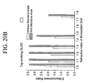
- FIGS. 20A-20C shows simulated emission for a device having a rectangular grid of a low-index material having a refractive index of 1.03.
- the thickness of the low-index regions is 100 nm
- the organic layers is 100 nm
- FIG. 20C shows that enhancement is optimized when the thickness of the LIG is the same as the thickness of the organic layers.
- the enhancement ratio may decrease as the thickness of the LIG decreases.
- FIG. 20A shows that the enhancement ratio increases as the width of the organic region ( w org ) decreases since more light in waveguide mode is outcoupled by entering the LIG prior to absorption in the organic and ITO layers.
- FIG. 20A also shows that the enhancement ratio increases as the width of the LIG increases ( w LIG ) since more light may be extracted out of waveguide mode without re-entering the organic layers.
- the width of the organic layer in such simulated emissions cannot be too small to ensure that the effective emitting area is sufficient for the device to achieve the required brightness.
- the width of the LIG is 1 ⁇ m and the organic layers is 6 ⁇ m, giving an effective lighting area of over 70%.
- FIG. 20B shows that the outcoupling efficiency of a top-emitting OLED increases with decreasing index of the LIG. As the refractive index of the LIG increases, more light is converted to glass mode and less is converted to air mode.
- FIG. 21 shows an exemplary device having a microlens sheet 610 e disposed adjacent to the substrate, or the substrate may include a microlens or microlens sheet.
- FIG. 20B shows the simulated enhancement of light as a function of the index of refraction for a top emitting OLED with an LIG (open bars) and with an LIG and a microlens (shaded bars). The outcoupling efficiency for such devices may be enhanced by a factor of about 2-3.
- FIGS. 14-17 show simulated results for variations in various device parameters. Unless indicated otherwise, each device was modeled with low-index regions 0.8 ⁇ m wide in a 1D periodic grid, organic emissive regions 4 ⁇ m wide, a 100 nm thick ITO electrode, and a low-index material refractive index of 1.03.
- FIG. 14 shows the proportion of light in air mode (squares) and glass mode (circles) as a function of ITO thickness, for thicknesses ranging from 70 to 150 nm.
- FIG. 14 shows the proportion of light in air mode (squares) and glass mode (circles) as a function of ITO thickness, for thicknesses ranging from 70 to 150 nm.
- FIG. 15 shows the proportion of light in each mode for low-index regions of varying width, from 500 to 1200 nm.
- FIG. 16 shows the proportion of light in each mode for organic regions from 4 ⁇ m to 10 ⁇ m.
- FIG. 17 shows the proportion of light in each mode for low-index material refractive indices of 1 to 1.75, for square and hexagonal grids. Values are shown for air mode for an ideal 1D periodic grid 1710, a square grid 1720, and a hexagonal grid 1730, and for glass mode for an ideal 1D periodic grid 1740, a square grid 1750, and a hexagonal grid 1760. The values indicated by the dotted oval are the same as those for a conventional OLED.
- a conventional OLED typically demonstrates proportions of about 0.17 light in air mode and 0.26 in glass mode.
- CBP 4,4'-N,N-dicarbazole-biphenyl m-MTDATA 4,4',4"-tris(3-methylphenylphenlyamino)triphenylamine
- Alq 3 8-tris-hydroxyquinoline aluminum
- Bphen 4,7-diphenyl-1,10-phenanthroline
- F 4 -TCNQ tetrafluoro-tetracyano-quinodimethane
- Ir(ppy) 3 tris(2-phenylpyridine)-iridium
- BCP 2,9-dimethyl-4,7-diphenyl-1,10-phenanthroline
- CuPc copper phthalocyanine.
- ITO indium tin oxide
- NPD N,N'-diphenyl-N-N'-di(1-naphthyl)-benzidine
- TPD N,N'-diphenyl-N-N'-di(3-toly)-benzidine
- mCP 1,3-N,N-dicarbazole-benzene
- DCM 4-(dicyanoethylene)-6-(4-dimethylaminostyryl-2-methyl)-4H-pyran
- DMQA N,N'-dimethylquinacridone
- PEDOT PSS : an aqueous dispersion of poly(3,4-ethylenedioxythiophene) with polystyrenesulfonate (PSS)
Landscapes
- Physics & Mathematics (AREA)
- Optics & Photonics (AREA)
- Electroluminescent Light Sources (AREA)
Claims (9)
- Dispositif (300) comprenant :un substrat (304) ;une première électrode (303) placée sur le substrat (304) ;une première couche placée sur la première électrode (303), la couche comprenant :une première région comprenant un matériau émissif organique (305) ; etune deuxième région comprenant un matériau à faible indice (310) présentant un indice de réfraction qui est inférieur à l'indice de réfraction du matériau émissif organique (305) ; et la deuxième région étant placée adjacente à la première région ; etune deuxième électrode (301) placée sur la première couche ;dans lequel au moins l'une des première et deuxième électrodes (303, 301) est une électrode transparente.
- Dispositif (300) selon la revendication 1, dans lequel le dispositif (300) est une OLED à transmission par le haut.
- Dispositif (300) selon la revendication 1, dans lequel le matériau à faible indice a un indice de réfraction de 1,0 à 3,0.
- Dispositif (300) selon la revendication 3, dans lequel le matériau à faible indice a un indice de réfraction de 1,0 à 1,5.
- Dispositif (300) selon la revendication 4, dans lequel le matériau à faible indice (310) forme un réseau orienté dans un plan parallèle à la première électrode (303) et à la deuxième électrode (301).
- Dispositif (300) selon la revendication 5, dans lequel le réseau est disposé avec une périodicité supérieure à la longueur d'onde de la lumière.
- Dispositif (300) selon la revendication 1, comprenant de plus une feuille de microlentilles placée sous le substrat, de sorte qu'une face convexe de la feuille de microlentilles est tournée dans la direction opposée au substrat.
- Dispositif (300) selon la revendication 1, dans lequel le matériau à faible indice (310) est choisi parmi le groupe composé d'un aérogel, du Téflon, d'un film calibré de SiO2, d'un film calibré de TiO2, et de couches de nano-tiges de SiO2.
- Procédé de fabrication d'un dispositif (300) émetteur de lumière, comprenant :le dépôt d'une première électrode (303) sur un substrat (304) ;le dépôt d'un réseau d'un matériau transparent à faible indice (310) ayant un indice de réfraction de 1,0 à 1,5 sur la première électrode (303);le dépôt d'un matériau émissif organique (305) sur le réseau, de sorte que le matériau émissif organique (305) soit en contact direct avec la première électrode (303), etle dépôt d'une deuxième électrode (301) sur le matériau émissif organique (305).
Priority Applications (1)
| Application Number | Priority Date | Filing Date | Title |
|---|---|---|---|
| EP12000004.7A EP2439806B1 (fr) | 2007-03-30 | 2008-03-31 | Oled avec couplage de sortie de lumière optimisé |
Applications Claiming Priority (4)
| Application Number | Priority Date | Filing Date | Title |
|---|---|---|---|
| US11/729,877 US20080238310A1 (en) | 2007-03-30 | 2007-03-30 | OLED with improved light outcoupling |
| US7032908P | 2008-03-21 | 2008-03-21 | |
| PCT/US2008/004242 WO2008121414A1 (fr) | 2007-03-30 | 2008-03-31 | Oled avec couplage de sortie de lumière optimisé |
| US12/059,783 US20080265757A1 (en) | 2007-03-30 | 2008-03-31 | Low Index Grids (LIG) To Increase Outcoupled Light From Top or Transparent OLED |
Related Child Applications (2)
| Application Number | Title | Priority Date | Filing Date |
|---|---|---|---|
| EP12000004.7A Division EP2439806B1 (fr) | 2007-03-30 | 2008-03-31 | Oled avec couplage de sortie de lumière optimisé |
| EP12000004.7 Division-Into | 2012-01-02 |
Publications (2)
| Publication Number | Publication Date |
|---|---|
| EP2132802A1 EP2132802A1 (fr) | 2009-12-16 |
| EP2132802B1 true EP2132802B1 (fr) | 2013-01-09 |
Family
ID=39687048
Family Applications (2)
| Application Number | Title | Priority Date | Filing Date |
|---|---|---|---|
| EP12000004.7A Active EP2439806B1 (fr) | 2007-03-30 | 2008-03-31 | Oled avec couplage de sortie de lumière optimisé |
| EP08742456A Active EP2132802B1 (fr) | 2007-03-30 | 2008-03-31 | Oled avec couplage de sortie de lumière optimisé |
Family Applications Before (1)
| Application Number | Title | Priority Date | Filing Date |
|---|---|---|---|
| EP12000004.7A Active EP2439806B1 (fr) | 2007-03-30 | 2008-03-31 | Oled avec couplage de sortie de lumière optimisé |
Country Status (7)
| Country | Link |
|---|---|
| US (1) | US20080265757A1 (fr) |
| EP (2) | EP2439806B1 (fr) |
| JP (2) | JP5662141B2 (fr) |
| KR (1) | KR101499043B1 (fr) |
| CN (1) | CN102769106A (fr) |
| RU (1) | RU2470415C2 (fr) |
| WO (1) | WO2008121414A1 (fr) |
Families Citing this family (37)
| Publication number | Priority date | Publication date | Assignee | Title |
|---|---|---|---|---|
| US8697254B2 (en) * | 2006-11-14 | 2014-04-15 | Sri International | Cavity electroluminescent devices and methods for producing the same |
| JP2010537427A (ja) | 2007-08-23 | 2010-12-02 | エスアールアイ インターナショナル | 有機カソードを用いるエレクトロルミネッセントデバイス |
| JP5552433B2 (ja) * | 2008-01-24 | 2014-07-16 | エスアールアイ インターナショナル | 高効率エレクトロルミネセント素子およびそれを生産するための方法 |
| US8310150B2 (en) * | 2009-02-04 | 2012-11-13 | The Regents Of The University Of Michigan | Light emitting device with high outcoupling |
| WO2011027276A1 (fr) | 2009-09-04 | 2011-03-10 | Koninklijke Philips Electronics N.V. | Dispositif delo à matériau à faible indice |
| KR101074804B1 (ko) * | 2009-11-24 | 2011-10-19 | 한국과학기술원 | 유기 발광 소자, 이를 포함하는 조명장치, 및 이를 포함하는 유기 발광 디스플레이 장치 |
| KR101084178B1 (ko) * | 2009-12-14 | 2011-11-17 | 한국과학기술원 | 유기 발광 소자, 이를 포함하는 조명 장치, 및 이를 포함하는 유기 발광 디스플레이 장치 |
| CN102110778B (zh) * | 2009-12-25 | 2013-07-10 | 昆山维信诺显示技术有限公司 | 一种有机电致发光器件 |
| US8729581B2 (en) * | 2010-01-13 | 2014-05-20 | Apple Inc. | Light guide for LED source |
| JP5258817B2 (ja) * | 2010-03-02 | 2013-08-07 | 株式会社東芝 | 照明装置及びその製造方法 |
| EP2824726B1 (fr) | 2010-04-28 | 2020-12-23 | Beijing Xiaomi Mobile Software Co., Ltd. | Dispositif électroluminescent organique |
| FR2964254B1 (fr) | 2010-08-30 | 2013-06-14 | Saint Gobain | Support de dispositif a diode electroluminescente organique, un tel dispositif a diode electroluminescente organique et son procede de fabrication |
| WO2012038876A1 (fr) | 2010-09-22 | 2012-03-29 | Koninklijke Philips Electronics N.V. | Dispositif d'affichage multi-vue |
| EP2495783A1 (fr) | 2011-03-01 | 2012-09-05 | Nederlandse Organisatie voor toegepast -natuurwetenschappelijk onderzoek TNO | Dispositif électroluminescent et son procédé de fabrication |
| JP5954651B2 (ja) * | 2011-12-09 | 2016-07-20 | 株式会社Joled | 表示装置および電子機器 |
| KR102023795B1 (ko) * | 2012-05-09 | 2019-09-20 | 메르크 파텐트 게엠베하 | 나노로드들의 형광 에미션에 기반한 3차원 디스플레이 시스템 |
| US9991463B2 (en) * | 2012-06-14 | 2018-06-05 | Universal Display Corporation | Electronic devices with improved shelf lives |
| WO2013186916A1 (fr) * | 2012-06-15 | 2013-12-19 | パイオニア株式会社 | Dispositif électroluminescent organique |
| KR20140017728A (ko) | 2012-07-31 | 2014-02-12 | 삼성디스플레이 주식회사 | 유기발광 표시장치 및 그 제조방법 |
| KR102051103B1 (ko) | 2012-11-07 | 2019-12-03 | 삼성디스플레이 주식회사 | 유기 발광 표시 장치 |
| FR3003084B1 (fr) * | 2013-03-08 | 2015-02-27 | Saint Gobain | Support electroconducteur pour oled, oled l'incorporant, et sa fabrication |
| CN104078613A (zh) * | 2013-03-29 | 2014-10-01 | 海洋王照明科技股份有限公司 | 白光有机电致发光器件及其制备方法 |
| US10468633B2 (en) * | 2013-06-05 | 2019-11-05 | Universal Display Corporation | Microlens array architectures for enhanced light outcoupling from an OLED array |
| US9385348B2 (en) | 2013-08-29 | 2016-07-05 | The Regents Of The University Of Michigan | Organic electronic devices with multiple solution-processed layers |
| KR20160047571A (ko) * | 2013-08-29 | 2016-05-02 | 더 리젠츠 오브 더 유니버시티 오브 미시간 | 다중의 용액 가공된 층을 지닌 유기 전자 디바이스 |
| RU2655461C2 (ru) * | 2013-12-26 | 2018-05-28 | Витро, С.А.Б. Де С.В. | Органический светоизлучающий диод с испускающим свет электродом |
| JP6548359B2 (ja) | 2014-05-12 | 2019-07-24 | キヤノン株式会社 | 有機発光素子 |
| KR102402679B1 (ko) | 2015-05-11 | 2022-05-27 | 삼성디스플레이 주식회사 | 표시 장치 |
| KR102395919B1 (ko) | 2015-06-19 | 2022-05-10 | 삼성디스플레이 주식회사 | 유기발광 표시장치 |
| US12006441B2 (en) * | 2015-10-20 | 2024-06-11 | Koninklijke Philips N.V. | Imprinting ink composition, imprinting method, optical element lighting device, optical sensor and photovoltaic device |
| DE102016009067A1 (de) | 2016-07-27 | 2018-02-15 | Docter Optics Se | Scheinwerferlinse für einen Kraftfahrzeugscheinwerfer |
| US20180097202A1 (en) * | 2016-10-03 | 2018-04-05 | Regents Of The University Of Michigan | Enhanced oled outcoupling by suppressing surface plasmon modes |
| KR102589906B1 (ko) * | 2016-10-31 | 2023-10-13 | 엘지디스플레이 주식회사 | 유기발광 표시장치 |
| DE102017004562A1 (de) | 2017-05-14 | 2018-11-15 | Docter Optics Se | Verfahren zum Herstellen eines Mikroprojektors und eines Projektionsdisplays |
| RU2746849C1 (ru) * | 2020-08-27 | 2021-04-21 | Федеральное государственное автономное образовательное учреждение высшего образования "Национальный исследовательский Нижегородский государственный университет им. Н.И. Лобачевского" | Способ изготовления магниторезистивного спинового светодиода (варианты) |
| RU2757593C1 (ru) * | 2020-12-11 | 2021-10-19 | Федеральное государственное бюджетное образовательное учреждение высшего образования "Российский химико-технологический университет имени Д.И. Менделеева" | Люминофорный материал на основе металлорганических комплексов однородно распределенных в объеме аэрогеля и способ его получения |
| RU2764107C1 (ru) * | 2020-12-27 | 2022-01-13 | Федеральное государственное бюджетное образовательное учреждение высшего образования «Российский химико-технологический университет имени Д.И. Менделеева» (РХТУ им. Д.И. Менделеева) | Способ получения высокочистых комплексов 8-гидроксихинолина с металлами |
Family Cites Families (33)
| Publication number | Priority date | Publication date | Assignee | Title |
|---|---|---|---|---|
| GB8909011D0 (en) | 1989-04-20 | 1989-06-07 | Friend Richard H | Electroluminescent devices |
| JP2846571B2 (ja) * | 1994-02-25 | 1999-01-13 | 出光興産株式会社 | 有機エレクトロルミネッセンス素子 |
| US6548956B2 (en) | 1994-12-13 | 2003-04-15 | The Trustees Of Princeton University | Transparent contacts for organic devices |
| US5707745A (en) | 1994-12-13 | 1998-01-13 | The Trustees Of Princeton University | Multicolor organic light emitting devices |
| US5703436A (en) | 1994-12-13 | 1997-12-30 | The Trustees Of Princeton University | Transparent contacts for organic devices |
| US5844363A (en) | 1997-01-23 | 1998-12-01 | The Trustees Of Princeton Univ. | Vacuum deposited, non-polymeric flexible organic light emitting devices |
| KR100462723B1 (ko) | 1996-08-12 | 2004-12-20 | 더 트러스티즈 오브 프린스턴 유니버시티 | 가요성 유기발광장치 및 그것을 제조하는 방법 |
| US6013982A (en) | 1996-12-23 | 2000-01-11 | The Trustees Of Princeton University | Multicolor display devices |
| US6091195A (en) | 1997-02-03 | 2000-07-18 | The Trustees Of Princeton University | Displays having mesa pixel configuration |
| US5834893A (en) | 1996-12-23 | 1998-11-10 | The Trustees Of Princeton University | High efficiency organic light emitting devices with light directing structures |
| EP1026924A4 (fr) * | 1997-05-08 | 2005-07-20 | Sanyo Electric Co | Dispositif electroluminescent organique |
| US6303238B1 (en) | 1997-12-01 | 2001-10-16 | The Trustees Of Princeton University | OLEDs doped with phosphorescent compounds |
| US6337102B1 (en) | 1997-11-17 | 2002-01-08 | The Trustees Of Princeton University | Low pressure vapor phase deposition of organic thin films |
| US6087196A (en) | 1998-01-30 | 2000-07-11 | The Trustees Of Princeton University | Fabrication of organic semiconductor devices using ink jet printing |
| US6097147A (en) | 1998-09-14 | 2000-08-01 | The Trustees Of Princeton University | Structure for high efficiency electroluminescent device |
| GB9822963D0 (en) | 1998-10-20 | 1998-12-16 | Agner Erik | Improvements in or relating to chromatography |
| JP2000277260A (ja) * | 1999-03-23 | 2000-10-06 | Seiko Epson Corp | 発光装置 |
| JP4279971B2 (ja) * | 1999-11-10 | 2009-06-17 | パナソニック電工株式会社 | 発光素子 |
| US6294398B1 (en) | 1999-11-23 | 2001-09-25 | The Trustees Of Princeton University | Method for patterning devices |
| RU2214073C2 (ru) * | 1999-12-30 | 2003-10-10 | Общество с ограниченной ответственностью "Научно-производственное предприятие "Кристаллы и Технологии" | Источник белого света |
| JP4724281B2 (ja) * | 2000-09-14 | 2011-07-13 | キヤノン株式会社 | 表示装置 |
| US6703780B2 (en) * | 2001-01-16 | 2004-03-09 | General Electric Company | Organic electroluminescent device with a ceramic output coupler and method of making the same |
| US7053547B2 (en) * | 2001-11-29 | 2006-05-30 | Universal Display Corporation | Increased emission efficiency in organic light-emitting devices on high-index substrates |
| JP4182467B2 (ja) * | 2001-12-27 | 2008-11-19 | セイコーエプソン株式会社 | 回路基板、電気光学装置及び電子機器 |
| US20030230980A1 (en) | 2002-06-18 | 2003-12-18 | Forrest Stephen R | Very low voltage, high efficiency phosphorescent oled in a p-i-n structure |
| US6831407B2 (en) * | 2002-10-15 | 2004-12-14 | Eastman Kodak Company | Oled device having improved light output |
| US7492092B2 (en) * | 2002-12-17 | 2009-02-17 | Seiko Epson Corporation | Self-emitting element, display panel, display apparatus, and method of manufacturing self-emitting element |
| JP2004241130A (ja) * | 2003-02-03 | 2004-08-26 | Seiko Epson Corp | 発光ディスプレイパネルおよびその製造方法 |
| JP2004296219A (ja) * | 2003-03-26 | 2004-10-21 | Fuji Photo Film Co Ltd | 発光素子 |
| JP5005164B2 (ja) * | 2004-03-03 | 2012-08-22 | 株式会社ジャパンディスプレイイースト | 発光素子,発光型表示装置及び照明装置 |
| JP4340199B2 (ja) * | 2004-07-09 | 2009-10-07 | セイコーエプソン株式会社 | 有機エレクトロルミネッセンス装置の製造方法 |
| JP4511440B2 (ja) * | 2004-10-05 | 2010-07-28 | 三星モバイルディスプレイ株式會社 | 有機発光素子及び有機発光素子の製造方法 |
| US7432649B2 (en) * | 2005-02-22 | 2008-10-07 | Corning, Incorporated | Coupled waveguides for light extraction |
-
2008
- 2008-03-31 EP EP12000004.7A patent/EP2439806B1/fr active Active
- 2008-03-31 CN CN2012102866866A patent/CN102769106A/zh active Pending
- 2008-03-31 EP EP08742456A patent/EP2132802B1/fr active Active
- 2008-03-31 KR KR1020097020391A patent/KR101499043B1/ko active IP Right Grant
- 2008-03-31 JP JP2010501024A patent/JP5662141B2/ja active Active
- 2008-03-31 RU RU2009135278/28A patent/RU2470415C2/ru active
- 2008-03-31 WO PCT/US2008/004242 patent/WO2008121414A1/fr active Application Filing
- 2008-03-31 US US12/059,783 patent/US20080265757A1/en not_active Abandoned
-
2014
- 2014-08-14 JP JP2014165246A patent/JP6141808B2/ja active Active
Also Published As
| Publication number | Publication date |
|---|---|
| JP5662141B2 (ja) | 2015-01-28 |
| EP2439806A1 (fr) | 2012-04-11 |
| KR20090128437A (ko) | 2009-12-15 |
| JP2010524153A (ja) | 2010-07-15 |
| KR101499043B1 (ko) | 2015-03-05 |
| JP2014239065A (ja) | 2014-12-18 |
| RU2009135278A (ru) | 2011-05-10 |
| US20080265757A1 (en) | 2008-10-30 |
| RU2470415C2 (ru) | 2012-12-20 |
| JP6141808B2 (ja) | 2017-06-07 |
| CN102769106A (zh) | 2012-11-07 |
| EP2132802A1 (fr) | 2009-12-16 |
| EP2439806B1 (fr) | 2014-01-15 |
| WO2008121414A1 (fr) | 2008-10-09 |
Similar Documents
| Publication | Publication Date | Title |
|---|---|---|
| EP2132802B1 (fr) | Oled avec couplage de sortie de lumière optimisé | |
| US9508957B2 (en) | OLED with improved light outcoupling | |
| US20080238310A1 (en) | OLED with improved light outcoupling | |
| KR102320646B1 (ko) | 향상층(들)을 갖는 oled 디바이스 | |
| US12114552B2 (en) | Organic electroluminescent devices | |
| US11647647B2 (en) | Enhanced outcoupling from surface plasmon modes in corrugated OLEDs | |
| CN110289365B (zh) | 使用低折射率电介质的有机发光装置 | |
| US11217762B2 (en) | Surface-plasmon-pumped light emitting devices | |
| JP2007234254A (ja) | 有機エレクトロルミネッセンス素子及びその製造方法 | |
| US11362311B2 (en) | Sub-electrode microlens array for organic light emitting devices | |
| US11832475B2 (en) | Flexible electronic display device | |
| US8310150B2 (en) | Light emitting device with high outcoupling | |
| US20160204387A1 (en) | Thick-ETL OLEDs with Sub-ITO Grids with Improved Outcoupling | |
| Mikami et al. | 60.4 L: Late‐News paper: High efficiency 200‐lm/W green light emitting organic devices prepared on High‐Index of refraction substrate | |
| US20230092459A1 (en) | Purcell-Effect-Enhanced Organic Light Emitting Diodes with Sub-Electrode Microlens Array | |
| US20230413590A1 (en) | Organic electroluminescent devices | |
| BRPI0809502A2 (pt) | Diodo orgânico emissor de luz (oled) com acoplamento externo melhorado |
Legal Events
| Date | Code | Title | Description |
|---|---|---|---|
| PUAI | Public reference made under article 153(3) epc to a published international application that has entered the european phase |
Free format text: ORIGINAL CODE: 0009012 |
|
| 17P | Request for examination filed |
Effective date: 20090912 |
|
| AK | Designated contracting states |
Kind code of ref document: A1 Designated state(s): AT BE BG CH CY CZ DE DK EE ES FI FR GB GR HR HU IE IS IT LI LT LU LV MC MT NL NO PL PT RO SE SI SK TR |
|
| 17Q | First examination report despatched |
Effective date: 20100118 |
|
| RIN1 | Information on inventor provided before grant (corrected) |
Inventor name: SUN, YIRU Inventor name: FORREST, STEPHEN |
|
| DAX | Request for extension of the european patent (deleted) | ||
| GRAP | Despatch of communication of intention to grant a patent |
Free format text: ORIGINAL CODE: EPIDOSNIGR1 |
|
| GRAS | Grant fee paid |
Free format text: ORIGINAL CODE: EPIDOSNIGR3 |
|
| GRAA | (expected) grant |
Free format text: ORIGINAL CODE: 0009210 |
|
| AK | Designated contracting states |
Kind code of ref document: B1 Designated state(s): AT BE BG CH CY CZ DE DK EE ES FI FR GB GR HR HU IE IS IT LI LT LU LV MC MT NL NO PL PT RO SE SI SK TR |
|
| REG | Reference to a national code |
Ref country code: GB Ref legal event code: FG4D |
|
| REG | Reference to a national code |
Ref country code: CH Ref legal event code: EP Ref country code: AT Ref legal event code: REF Ref document number: 593200 Country of ref document: AT Kind code of ref document: T Effective date: 20130115 |
|
| REG | Reference to a national code |
Ref country code: IE Ref legal event code: FG4D |
|
| REG | Reference to a national code |
Ref country code: DE Ref legal event code: R096 Ref document number: 602008021545 Country of ref document: DE Effective date: 20130307 |
|
| PG25 | Lapsed in a contracting state [announced via postgrant information from national office to epo] |
Ref country code: SI Free format text: LAPSE BECAUSE OF FAILURE TO SUBMIT A TRANSLATION OF THE DESCRIPTION OR TO PAY THE FEE WITHIN THE PRESCRIBED TIME-LIMIT Effective date: 20130109 |
|
| REG | Reference to a national code |
Ref country code: NL Ref legal event code: VDEP Effective date: 20130109 |
|
| REG | Reference to a national code |
Ref country code: AT Ref legal event code: MK05 Ref document number: 593200 Country of ref document: AT Kind code of ref document: T Effective date: 20130109 |
|
| REG | Reference to a national code |
Ref country code: LT Ref legal event code: MG4D |
|
| PG25 | Lapsed in a contracting state [announced via postgrant information from national office to epo] |
Ref country code: IS Free format text: LAPSE BECAUSE OF FAILURE TO SUBMIT A TRANSLATION OF THE DESCRIPTION OR TO PAY THE FEE WITHIN THE PRESCRIBED TIME-LIMIT Effective date: 20130509 Ref country code: NO Free format text: LAPSE BECAUSE OF FAILURE TO SUBMIT A TRANSLATION OF THE DESCRIPTION OR TO PAY THE FEE WITHIN THE PRESCRIBED TIME-LIMIT Effective date: 20130409 Ref country code: AT Free format text: LAPSE BECAUSE OF FAILURE TO SUBMIT A TRANSLATION OF THE DESCRIPTION OR TO PAY THE FEE WITHIN THE PRESCRIBED TIME-LIMIT Effective date: 20130109 Ref country code: BE Free format text: LAPSE BECAUSE OF FAILURE TO SUBMIT A TRANSLATION OF THE DESCRIPTION OR TO PAY THE FEE WITHIN THE PRESCRIBED TIME-LIMIT Effective date: 20130109 Ref country code: ES Free format text: LAPSE BECAUSE OF FAILURE TO SUBMIT A TRANSLATION OF THE DESCRIPTION OR TO PAY THE FEE WITHIN THE PRESCRIBED TIME-LIMIT Effective date: 20130420 Ref country code: BG Free format text: LAPSE BECAUSE OF FAILURE TO SUBMIT A TRANSLATION OF THE DESCRIPTION OR TO PAY THE FEE WITHIN THE PRESCRIBED TIME-LIMIT Effective date: 20130409 Ref country code: SE Free format text: LAPSE BECAUSE OF FAILURE TO SUBMIT A TRANSLATION OF THE DESCRIPTION OR TO PAY THE FEE WITHIN THE PRESCRIBED TIME-LIMIT Effective date: 20130109 Ref country code: LT Free format text: LAPSE BECAUSE OF FAILURE TO SUBMIT A TRANSLATION OF THE DESCRIPTION OR TO PAY THE FEE WITHIN THE PRESCRIBED TIME-LIMIT Effective date: 20130109 |
|
| PG25 | Lapsed in a contracting state [announced via postgrant information from national office to epo] |
Ref country code: LV Free format text: LAPSE BECAUSE OF FAILURE TO SUBMIT A TRANSLATION OF THE DESCRIPTION OR TO PAY THE FEE WITHIN THE PRESCRIBED TIME-LIMIT Effective date: 20130109 Ref country code: PT Free format text: LAPSE BECAUSE OF FAILURE TO SUBMIT A TRANSLATION OF THE DESCRIPTION OR TO PAY THE FEE WITHIN THE PRESCRIBED TIME-LIMIT Effective date: 20130509 Ref country code: PL Free format text: LAPSE BECAUSE OF FAILURE TO SUBMIT A TRANSLATION OF THE DESCRIPTION OR TO PAY THE FEE WITHIN THE PRESCRIBED TIME-LIMIT Effective date: 20130109 Ref country code: FI Free format text: LAPSE BECAUSE OF FAILURE TO SUBMIT A TRANSLATION OF THE DESCRIPTION OR TO PAY THE FEE WITHIN THE PRESCRIBED TIME-LIMIT Effective date: 20130109 Ref country code: GR Free format text: LAPSE BECAUSE OF FAILURE TO SUBMIT A TRANSLATION OF THE DESCRIPTION OR TO PAY THE FEE WITHIN THE PRESCRIBED TIME-LIMIT Effective date: 20130410 Ref country code: NL Free format text: LAPSE BECAUSE OF FAILURE TO SUBMIT A TRANSLATION OF THE DESCRIPTION OR TO PAY THE FEE WITHIN THE PRESCRIBED TIME-LIMIT Effective date: 20130109 |
|
| PG25 | Lapsed in a contracting state [announced via postgrant information from national office to epo] |
Ref country code: HR Free format text: LAPSE BECAUSE OF FAILURE TO SUBMIT A TRANSLATION OF THE DESCRIPTION OR TO PAY THE FEE WITHIN THE PRESCRIBED TIME-LIMIT Effective date: 20130109 |
|
| REG | Reference to a national code |
Ref country code: DE Ref legal event code: R097 Ref document number: 602008021545 Country of ref document: DE |
|
| PG25 | Lapsed in a contracting state [announced via postgrant information from national office to epo] |
Ref country code: SK Free format text: LAPSE BECAUSE OF FAILURE TO SUBMIT A TRANSLATION OF THE DESCRIPTION OR TO PAY THE FEE WITHIN THE PRESCRIBED TIME-LIMIT Effective date: 20130109 Ref country code: EE Free format text: LAPSE BECAUSE OF FAILURE TO SUBMIT A TRANSLATION OF THE DESCRIPTION OR TO PAY THE FEE WITHIN THE PRESCRIBED TIME-LIMIT Effective date: 20130109 Ref country code: DK Free format text: LAPSE BECAUSE OF FAILURE TO SUBMIT A TRANSLATION OF THE DESCRIPTION OR TO PAY THE FEE WITHIN THE PRESCRIBED TIME-LIMIT Effective date: 20130109 Ref country code: RO Free format text: LAPSE BECAUSE OF FAILURE TO SUBMIT A TRANSLATION OF THE DESCRIPTION OR TO PAY THE FEE WITHIN THE PRESCRIBED TIME-LIMIT Effective date: 20130109 Ref country code: MC Free format text: LAPSE BECAUSE OF NON-PAYMENT OF DUE FEES Effective date: 20130331 Ref country code: CZ Free format text: LAPSE BECAUSE OF FAILURE TO SUBMIT A TRANSLATION OF THE DESCRIPTION OR TO PAY THE FEE WITHIN THE PRESCRIBED TIME-LIMIT Effective date: 20130109 |
|
| REG | Reference to a national code |
Ref country code: CH Ref legal event code: PL |
|
| PLBE | No opposition filed within time limit |
Free format text: ORIGINAL CODE: 0009261 |
|
| STAA | Information on the status of an ep patent application or granted ep patent |
Free format text: STATUS: NO OPPOSITION FILED WITHIN TIME LIMIT |
|
| PG25 | Lapsed in a contracting state [announced via postgrant information from national office to epo] |
Ref country code: CY Free format text: LAPSE BECAUSE OF FAILURE TO SUBMIT A TRANSLATION OF THE DESCRIPTION OR TO PAY THE FEE WITHIN THE PRESCRIBED TIME-LIMIT Effective date: 20130109 |
|
| 26N | No opposition filed |
Effective date: 20131010 |
|
| REG | Reference to a national code |
Ref country code: DE Ref legal event code: R082 Ref document number: 602008021545 Country of ref document: DE |
|
| PG25 | Lapsed in a contracting state [announced via postgrant information from national office to epo] |
Ref country code: IT Free format text: LAPSE BECAUSE OF FAILURE TO SUBMIT A TRANSLATION OF THE DESCRIPTION OR TO PAY THE FEE WITHIN THE PRESCRIBED TIME-LIMIT Effective date: 20130109 |
|
| REG | Reference to a national code |
Ref country code: IE Ref legal event code: MM4A |
|
| REG | Reference to a national code |
Ref country code: DE Ref legal event code: R097 Ref document number: 602008021545 Country of ref document: DE Effective date: 20131010 |
|
| PG25 | Lapsed in a contracting state [announced via postgrant information from national office to epo] |
Ref country code: LI Free format text: LAPSE BECAUSE OF NON-PAYMENT OF DUE FEES Effective date: 20130331 Ref country code: CH Free format text: LAPSE BECAUSE OF NON-PAYMENT OF DUE FEES Effective date: 20130331 Ref country code: IE Free format text: LAPSE BECAUSE OF NON-PAYMENT OF DUE FEES Effective date: 20130331 |
|
| PG25 | Lapsed in a contracting state [announced via postgrant information from national office to epo] |
Ref country code: MT Free format text: LAPSE BECAUSE OF FAILURE TO SUBMIT A TRANSLATION OF THE DESCRIPTION OR TO PAY THE FEE WITHIN THE PRESCRIBED TIME-LIMIT Effective date: 20130109 |
|
| PG25 | Lapsed in a contracting state [announced via postgrant information from national office to epo] |
Ref country code: TR Free format text: LAPSE BECAUSE OF FAILURE TO SUBMIT A TRANSLATION OF THE DESCRIPTION OR TO PAY THE FEE WITHIN THE PRESCRIBED TIME-LIMIT Effective date: 20130109 |
|
| PG25 | Lapsed in a contracting state [announced via postgrant information from national office to epo] |
Ref country code: HU Free format text: LAPSE BECAUSE OF FAILURE TO SUBMIT A TRANSLATION OF THE DESCRIPTION OR TO PAY THE FEE WITHIN THE PRESCRIBED TIME-LIMIT; INVALID AB INITIO Effective date: 20080331 Ref country code: LU Free format text: LAPSE BECAUSE OF NON-PAYMENT OF DUE FEES Effective date: 20130331 |
|
| REG | Reference to a national code |
Ref country code: FR Ref legal event code: PLFP Year of fee payment: 9 |
|
| REG | Reference to a national code |
Ref country code: FR Ref legal event code: PLFP Year of fee payment: 10 |
|
| REG | Reference to a national code |
Ref country code: FR Ref legal event code: PLFP Year of fee payment: 11 |
|
| REG | Reference to a national code |
Ref country code: DE Ref legal event code: R079 Ref document number: 602008021545 Country of ref document: DE Free format text: PREVIOUS MAIN CLASS: H01L0051520000 Ipc: H10K0050800000 |
|
| P01 | Opt-out of the competence of the unified patent court (upc) registered |
Effective date: 20230417 |
|
| PGFP | Annual fee paid to national office [announced via postgrant information from national office to epo] |
Ref country code: DE Payment date: 20240327 Year of fee payment: 17 Ref country code: GB Payment date: 20240327 Year of fee payment: 17 |
|
| PGFP | Annual fee paid to national office [announced via postgrant information from national office to epo] |
Ref country code: FR Payment date: 20240325 Year of fee payment: 17 |