EP2132802B1 - Oled mit verbesserter lichtauskopplung - Google Patents
Oled mit verbesserter lichtauskopplung Download PDFInfo
- Publication number
- EP2132802B1 EP2132802B1 EP08742456A EP08742456A EP2132802B1 EP 2132802 B1 EP2132802 B1 EP 2132802B1 EP 08742456 A EP08742456 A EP 08742456A EP 08742456 A EP08742456 A EP 08742456A EP 2132802 B1 EP2132802 B1 EP 2132802B1
- Authority
- EP
- European Patent Office
- Prior art keywords
- layer
- low
- index
- electrode
- light
- Prior art date
- Legal status (The legal status is an assumption and is not a legal conclusion. Google has not performed a legal analysis and makes no representation as to the accuracy of the status listed.)
- Active
Links
- 239000000463 material Substances 0.000 claims description 162
- 239000000758 substrate Substances 0.000 claims description 58
- 238000000151 deposition Methods 0.000 claims description 16
- VYPSYNLAJGMNEJ-UHFFFAOYSA-N Silicium dioxide Chemical compound O=[Si]=O VYPSYNLAJGMNEJ-UHFFFAOYSA-N 0.000 claims description 13
- 238000004519 manufacturing process Methods 0.000 claims description 7
- 239000004964 aerogel Substances 0.000 claims description 6
- 239000000377 silicon dioxide Substances 0.000 claims description 6
- 239000004809 Teflon Substances 0.000 claims description 5
- 229920006362 Teflon® Polymers 0.000 claims description 5
- GWEVSGVZZGPLCZ-UHFFFAOYSA-N Titan oxide Chemical compound O=[Ti]=O GWEVSGVZZGPLCZ-UHFFFAOYSA-N 0.000 claims description 4
- 229910052681 coesite Inorganic materials 0.000 claims description 4
- 229910052906 cristobalite Inorganic materials 0.000 claims description 4
- 229910052682 stishovite Inorganic materials 0.000 claims description 4
- 229910052905 tridymite Inorganic materials 0.000 claims description 4
- 239000002073 nanorod Substances 0.000 claims description 2
- 239000010410 layer Substances 0.000 description 169
- 239000012044 organic layer Substances 0.000 description 34
- 239000011521 glass Substances 0.000 description 28
- 230000032258 transport Effects 0.000 description 21
- 239000007924 injection Substances 0.000 description 20
- 238000002347 injection Methods 0.000 description 20
- 150000003384 small molecules Chemical class 0.000 description 19
- 239000011241 protective layer Substances 0.000 description 16
- 230000000903 blocking effect Effects 0.000 description 13
- 230000005525 hole transport Effects 0.000 description 13
- 239000011368 organic material Substances 0.000 description 12
- 238000000034 method Methods 0.000 description 11
- 238000004770 highest occupied molecular orbital Methods 0.000 description 10
- 229910052751 metal Inorganic materials 0.000 description 10
- 239000002184 metal Substances 0.000 description 10
- 229920000642 polymer Polymers 0.000 description 9
- 230000012447 hatching Effects 0.000 description 8
- 238000004768 lowest unoccupied molecular orbital Methods 0.000 description 7
- 239000000243 solution Substances 0.000 description 7
- 150000001875 compounds Chemical class 0.000 description 6
- 239000000412 dendrimer Substances 0.000 description 6
- 229920000736 dendritic polymer Polymers 0.000 description 6
- 239000002019 doping agent Substances 0.000 description 6
- 230000005693 optoelectronics Effects 0.000 description 6
- XCJYREBRNVKWGJ-UHFFFAOYSA-N copper(II) phthalocyanine Chemical compound [Cu+2].C12=CC=CC=C2C(N=C2[N-]C(C3=CC=CC=C32)=N2)=NC1=NC([C]1C=CC=CC1=1)=NC=1N=C1[C]3C=CC=CC3=C2[N-]1 XCJYREBRNVKWGJ-UHFFFAOYSA-N 0.000 description 5
- 238000009826 distribution Methods 0.000 description 5
- 230000008569 process Effects 0.000 description 5
- 239000010405 anode material Substances 0.000 description 4
- 239000002800 charge carrier Substances 0.000 description 4
- -1 e.g. Polymers 0.000 description 4
- 230000000694 effects Effects 0.000 description 4
- 230000007246 mechanism Effects 0.000 description 4
- 229910044991 metal oxide Inorganic materials 0.000 description 4
- 150000004706 metal oxides Chemical class 0.000 description 4
- 239000007787 solid Substances 0.000 description 4
- 125000001424 substituent group Chemical group 0.000 description 4
- 239000012780 transparent material Substances 0.000 description 4
- IXHWGNYCZPISET-UHFFFAOYSA-N 2-[4-(dicyanomethylidene)-2,3,5,6-tetrafluorocyclohexa-2,5-dien-1-ylidene]propanedinitrile Chemical compound FC1=C(F)C(=C(C#N)C#N)C(F)=C(F)C1=C(C#N)C#N IXHWGNYCZPISET-UHFFFAOYSA-N 0.000 description 3
- SCZWJXTUYYSKGF-UHFFFAOYSA-N 5,12-dimethylquinolino[2,3-b]acridine-7,14-dione Chemical compound CN1C2=CC=CC=C2C(=O)C2=C1C=C1C(=O)C3=CC=CC=C3N(C)C1=C2 SCZWJXTUYYSKGF-UHFFFAOYSA-N 0.000 description 3
- 230000007423 decrease Effects 0.000 description 3
- AMGQUBHHOARCQH-UHFFFAOYSA-N indium;oxotin Chemical compound [In].[Sn]=O AMGQUBHHOARCQH-UHFFFAOYSA-N 0.000 description 3
- UEEXRMUCXBPYOV-UHFFFAOYSA-N iridium;2-phenylpyridine Chemical compound [Ir].C1=CC=CC=C1C1=CC=CC=N1.C1=CC=CC=C1C1=CC=CC=N1.C1=CC=CC=C1C1=CC=CC=N1 UEEXRMUCXBPYOV-UHFFFAOYSA-N 0.000 description 3
- 239000000203 mixture Substances 0.000 description 3
- 229910052757 nitrogen Inorganic materials 0.000 description 3
- 230000003287 optical effect Effects 0.000 description 3
- 230000000737 periodic effect Effects 0.000 description 3
- 229920003023 plastic Polymers 0.000 description 3
- 239000004033 plastic Substances 0.000 description 3
- 239000002356 single layer Substances 0.000 description 3
- 238000001228 spectrum Methods 0.000 description 3
- 239000000126 substance Substances 0.000 description 3
- TVIVIEFSHFOWTE-UHFFFAOYSA-K tri(quinolin-8-yloxy)alumane Chemical compound [Al+3].C1=CN=C2C([O-])=CC=CC2=C1.C1=CN=C2C([O-])=CC=CC2=C1.C1=CN=C2C([O-])=CC=CC2=C1 TVIVIEFSHFOWTE-UHFFFAOYSA-K 0.000 description 3
- DHDHJYNTEFLIHY-UHFFFAOYSA-N 4,7-diphenyl-1,10-phenanthroline Chemical group C1=CC=CC=C1C1=CC=NC2=C1C=CC1=C(C=3C=CC=CC=3)C=CN=C21 DHDHJYNTEFLIHY-UHFFFAOYSA-N 0.000 description 2
- DIVZFUBWFAOMCW-UHFFFAOYSA-N 4-n-(3-methylphenyl)-1-n,1-n-bis[4-(n-(3-methylphenyl)anilino)phenyl]-4-n-phenylbenzene-1,4-diamine Chemical group CC1=CC=CC(N(C=2C=CC=CC=2)C=2C=CC(=CC=2)N(C=2C=CC(=CC=2)N(C=2C=CC=CC=2)C=2C=C(C)C=CC=2)C=2C=CC(=CC=2)N(C=2C=CC=CC=2)C=2C=C(C)C=CC=2)=C1 DIVZFUBWFAOMCW-UHFFFAOYSA-N 0.000 description 2
- IJGRMHOSHXDMSA-UHFFFAOYSA-N Atomic nitrogen Chemical compound N#N IJGRMHOSHXDMSA-UHFFFAOYSA-N 0.000 description 2
- LFQSCWFLJHTTHZ-UHFFFAOYSA-N Ethanol Chemical compound CCO LFQSCWFLJHTTHZ-UHFFFAOYSA-N 0.000 description 2
- 229920000144 PEDOT:PSS Polymers 0.000 description 2
- 125000000217 alkyl group Chemical group 0.000 description 2
- 239000010406 cathode material Substances 0.000 description 2
- 230000008859 change Effects 0.000 description 2
- 230000008021 deposition Effects 0.000 description 2
- 238000010586 diagram Methods 0.000 description 2
- JAONJTDQXUSBGG-UHFFFAOYSA-N dialuminum;dizinc;oxygen(2-) Chemical compound [O-2].[O-2].[O-2].[O-2].[O-2].[Al+3].[Al+3].[Zn+2].[Zn+2] JAONJTDQXUSBGG-UHFFFAOYSA-N 0.000 description 2
- 238000000295 emission spectrum Methods 0.000 description 2
- 125000001183 hydrocarbyl group Chemical group 0.000 description 2
- 238000005286 illumination Methods 0.000 description 2
- 239000007788 liquid Substances 0.000 description 2
- 239000011159 matrix material Substances 0.000 description 2
- 150000002739 metals Chemical class 0.000 description 2
- 238000000059 patterning Methods 0.000 description 2
- 229920001467 poly(styrenesulfonates) Polymers 0.000 description 2
- 229960002796 polystyrene sulfonate Drugs 0.000 description 2
- 239000011970 polystyrene sulfonate Substances 0.000 description 2
- 229910052710 silicon Inorganic materials 0.000 description 2
- 239000010703 silicon Substances 0.000 description 2
- 238000010129 solution processing Methods 0.000 description 2
- 238000002207 thermal evaporation Methods 0.000 description 2
- 125000001637 1-naphthyl group Chemical group [H]C1=C([H])C([H])=C2C(*)=C([H])C([H])=C([H])C2=C1[H] 0.000 description 1
- STTGYIUESPWXOW-UHFFFAOYSA-N 2,9-dimethyl-4,7-diphenyl-1,10-phenanthroline Chemical compound C=12C=CC3=C(C=4C=CC=CC=4)C=C(C)N=C3C2=NC(C)=CC=1C1=CC=CC=C1 STTGYIUESPWXOW-UHFFFAOYSA-N 0.000 description 1
- OKTJSMMVPCPJKN-UHFFFAOYSA-N Carbon Chemical compound [C] OKTJSMMVPCPJKN-UHFFFAOYSA-N 0.000 description 1
- 229920001609 Poly(3,4-ethylenedioxythiophene) Polymers 0.000 description 1
- 239000004965 Silica aerogel Substances 0.000 description 1
- XUIMIQQOPSSXEZ-UHFFFAOYSA-N Silicon Chemical compound [Si] XUIMIQQOPSSXEZ-UHFFFAOYSA-N 0.000 description 1
- 239000007983 Tris buffer Substances 0.000 description 1
- 238000010521 absorption reaction Methods 0.000 description 1
- 229910052782 aluminium Inorganic materials 0.000 description 1
- XAGFODPZIPBFFR-UHFFFAOYSA-N aluminium Chemical compound [Al] XAGFODPZIPBFFR-UHFFFAOYSA-N 0.000 description 1
- PNEYBMLMFCGWSK-UHFFFAOYSA-N aluminium oxide Inorganic materials [O-2].[O-2].[O-2].[Al+3].[Al+3] PNEYBMLMFCGWSK-UHFFFAOYSA-N 0.000 description 1
- 125000003118 aryl group Chemical group 0.000 description 1
- 230000004888 barrier function Effects 0.000 description 1
- UHOVQNZJYSORNB-UHFFFAOYSA-N benzene Substances C1=CC=CC=C1 UHOVQNZJYSORNB-UHFFFAOYSA-N 0.000 description 1
- 239000004305 biphenyl Substances 0.000 description 1
- 229910052799 carbon Inorganic materials 0.000 description 1
- 238000006243 chemical reaction Methods 0.000 description 1
- 239000000470 constituent Substances 0.000 description 1
- 229920001577 copolymer Polymers 0.000 description 1
- 238000010168 coupling process Methods 0.000 description 1
- 238000005859 coupling reaction Methods 0.000 description 1
- 230000003247 decreasing effect Effects 0.000 description 1
- 239000006185 dispersion Substances 0.000 description 1
- 239000007772 electrode material Substances 0.000 description 1
- 238000005516 engineering process Methods 0.000 description 1
- 238000000605 extraction Methods 0.000 description 1
- 239000011888 foil Substances 0.000 description 1
- 239000007789 gas Substances 0.000 description 1
- 238000009499 grossing Methods 0.000 description 1
- RBTKNAXYKSUFRK-UHFFFAOYSA-N heliogen blue Chemical compound [Cu].[N-]1C2=C(C=CC=C3)C3=C1N=C([N-]1)C3=CC=CC=C3C1=NC([N-]1)=C(C=CC=C3)C3=C1N=C([N-]1)C3=CC=CC=C3C1=N2 RBTKNAXYKSUFRK-UHFFFAOYSA-N 0.000 description 1
- 239000003446 ligand Substances 0.000 description 1
- 230000000877 morphologic effect Effects 0.000 description 1
- IBHBKWKFFTZAHE-UHFFFAOYSA-N n-[4-[4-(n-naphthalen-1-ylanilino)phenyl]phenyl]-n-phenylnaphthalen-1-amine Chemical compound C1=CC=CC=C1N(C=1C2=CC=CC=C2C=CC=1)C1=CC=C(C=2C=CC(=CC=2)N(C=2C=CC=CC=2)C=2C3=CC=CC=C3C=CC=2)C=C1 IBHBKWKFFTZAHE-UHFFFAOYSA-N 0.000 description 1
- 238000005457 optimization Methods 0.000 description 1
- 238000013086 organic photovoltaic Methods 0.000 description 1
- 230000001151 other effect Effects 0.000 description 1
- 239000002243 precursor Substances 0.000 description 1
- 238000007639 printing Methods 0.000 description 1
- 230000001902 propagating effect Effects 0.000 description 1
- 239000004065 semiconductor Substances 0.000 description 1
- 230000011664 signaling Effects 0.000 description 1
- 235000012239 silicon dioxide Nutrition 0.000 description 1
- 238000003980 solgel method Methods 0.000 description 1
- 238000004528 spin coating Methods 0.000 description 1
- 239000000725 suspension Substances 0.000 description 1
- 230000002195 synergetic effect Effects 0.000 description 1
- ODHXBMXNKOYIBV-UHFFFAOYSA-N triphenylamine Chemical compound C1=CC=CC=C1N(C=1C=CC=CC=1)C1=CC=CC=C1 ODHXBMXNKOYIBV-UHFFFAOYSA-N 0.000 description 1
- 238000001947 vapour-phase growth Methods 0.000 description 1
- 239000003981 vehicle Substances 0.000 description 1
- 238000003466 welding Methods 0.000 description 1
- 238000009736 wetting Methods 0.000 description 1
- YVTHLONGBIQYBO-UHFFFAOYSA-N zinc indium(3+) oxygen(2-) Chemical compound [O--].[Zn++].[In+3] YVTHLONGBIQYBO-UHFFFAOYSA-N 0.000 description 1
Images


Classifications
-
- H—ELECTRICITY
- H10—SEMICONDUCTOR DEVICES; ELECTRIC SOLID-STATE DEVICES NOT OTHERWISE PROVIDED FOR
- H10K—ORGANIC ELECTRIC SOLID-STATE DEVICES
- H10K50/00—Organic light-emitting devices
- H10K50/80—Constructional details
- H10K50/85—Arrangements for extracting light from the devices
- H10K50/858—Arrangements for extracting light from the devices comprising refractive means, e.g. lenses
Claims (9)
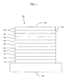
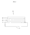
- Eine Einrichtung (300), umfassend:ein Substrat (304);eine erste Elektrode (303), die über dem Substrat (304) angeordnet ist;eine erste, über der ersten Elektrode (303) angeordnete Lage, wobei diese Lage umfasst:- -einen ersten Bereich, umfassend ein organisches emittierendes Material (305); und- einen zweiten Bereich umfassend ein Niedrig-Index-Material (310), das einen Brechungsindex aufweist, der kleiner ist als der Brechungsindex des organischen emittierenden Materials (305); und wobei der zweite Bereich benachbart zu dem ersten Bereich angeordnet ist; undeine zweite Elektrode (301), die über der ersten Lage abgelagert ist;wobei wenigstens eine der ersten und zweiten Elektroden (303,301) eine transparente Elektrode ist.
- Die Einrichtung (300) nach Anspruch 1, worin die Einrichtung (300) eine oben aussendende OLED ist.
- Die Einrichtung (300) nach Anspruch 1, worin das Niedrig-Index-Material einen Brechungsindex von 1.0 bis 3.0 aufweist.
- Die Einrichtung (300) nach Anspruch 3, worin das Niedrig-Index-Material einen Brechungsindex von 1.0 bis 1.5 aufweist.
- Die Einrichtung (300) nach Anspruch 4, worin das Niedrig-Index-Material (310) ein Gitter bildet, das in einer Ebene parallel zu der ersten Elektrode (303) und zu der zweiten Elektrode (301) ausgerichtet ist.
- Die Einrichtung (300) nach Anspruch 5, worin das Gitter mit einer Periodizität ausgelegt ist, die größer als die Wellenlänge von Licht ist.
- Die Einrichtung (300) nach Anspruch 1, weiter umfassend ein Mikrolinsen-Blatt, das unter dem Substrat derart angeordnet ist, dass eine konvexe Seite der Mikrolinse in die dem Substrat entgegengesetzte Richtung zeigt.
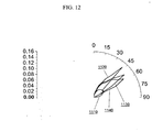
- Die Einrichtung (300) nach Anspruch 1, worin das Niedrig-Index-Material (310) aus der Gruppe ausgewählt ist, die aus Aerogel, Teflon, einer gradierten /gestuften Dünnschicht SiO2, einer gradierten / gestuften Dünnschicht TiO2, und Lagen von SiO2 Nano-Stäbchen besteht.
- Ein Verfahren zum Herstellen einer Licht emittierenden Einrichtung (300), umfassend:Ablagern einer ersten Elektrode (303) über einem Substrat (304);Ablagern eines Gitters aus transparentem Niedrig-Index-Material (310) mit einem Brechungsindex von 1.0 bis 1.5 über der ersten Elektrode (303);Ablagern eines organischen emittierenden Materials (305) über dem Gitter derart, dass sich das emittierende Material (305) in direktem Kontakt mit der ersten Elektrode (303) befindet, und Ablagern einer zweiten Elektrode (301) über dem organischen emittierenden Material (305).
Priority Applications (1)
| Application Number | Priority Date | Filing Date | Title |
|---|---|---|---|
| EP12000004.7A EP2439806B1 (de) | 2007-03-30 | 2008-03-31 | Oled mit verbesserter lichtauskopplung |
Applications Claiming Priority (4)
| Application Number | Priority Date | Filing Date | Title |
|---|---|---|---|
| US11/729,877 US20080238310A1 (en) | 2007-03-30 | 2007-03-30 | OLED with improved light outcoupling |
| US7032908P | 2008-03-21 | 2008-03-21 | |
| PCT/US2008/004242 WO2008121414A1 (en) | 2007-03-30 | 2008-03-31 | Oled with improved light outcoupling |
| US12/059,783 US20080265757A1 (en) | 2007-03-30 | 2008-03-31 | Low Index Grids (LIG) To Increase Outcoupled Light From Top or Transparent OLED |
Related Child Applications (2)
| Application Number | Title | Priority Date | Filing Date |
|---|---|---|---|
| EP12000004.7A Division EP2439806B1 (de) | 2007-03-30 | 2008-03-31 | Oled mit verbesserter lichtauskopplung |
| EP12000004.7 Division-Into | 2012-01-02 |
Publications (2)
| Publication Number | Publication Date |
|---|---|
| EP2132802A1 EP2132802A1 (de) | 2009-12-16 |
| EP2132802B1 true EP2132802B1 (de) | 2013-01-09 |
Family
ID=39687048
Family Applications (2)
| Application Number | Title | Priority Date | Filing Date |
|---|---|---|---|
| EP12000004.7A Active EP2439806B1 (de) | 2007-03-30 | 2008-03-31 | Oled mit verbesserter lichtauskopplung |
| EP08742456A Active EP2132802B1 (de) | 2007-03-30 | 2008-03-31 | Oled mit verbesserter lichtauskopplung |
Family Applications Before (1)
| Application Number | Title | Priority Date | Filing Date |
|---|---|---|---|
| EP12000004.7A Active EP2439806B1 (de) | 2007-03-30 | 2008-03-31 | Oled mit verbesserter lichtauskopplung |
Country Status (7)
| Country | Link |
|---|---|
| US (1) | US20080265757A1 (de) |
| EP (2) | EP2439806B1 (de) |
| JP (2) | JP5662141B2 (de) |
| KR (1) | KR101499043B1 (de) |
| CN (1) | CN102769106A (de) |
| RU (1) | RU2470415C2 (de) |
| WO (1) | WO2008121414A1 (de) |
Families Citing this family (37)
| Publication number | Priority date | Publication date | Assignee | Title |
|---|---|---|---|---|
| US8697254B2 (en) * | 2006-11-14 | 2014-04-15 | Sri International | Cavity electroluminescent devices and methods for producing the same |
| KR20100076950A (ko) | 2007-08-23 | 2010-07-06 | 에스알아이 인터내셔널 | 유기 음극을 사용하는 전장발광 장치 |
| EP2238635B1 (de) * | 2008-01-24 | 2012-07-04 | SRI International | Hochleistungselektrolumineszenzvorrichtungen und herstellungsverfahren dafür |
| US8310150B2 (en) * | 2009-02-04 | 2012-11-13 | The Regents Of The University Of Michigan | Light emitting device with high outcoupling |
| WO2011027276A1 (en) | 2009-09-04 | 2011-03-10 | Koninklijke Philips Electronics N.V. | Oled device with low index material |
| KR101074804B1 (ko) * | 2009-11-24 | 2011-10-19 | 한국과학기술원 | 유기 발광 소자, 이를 포함하는 조명장치, 및 이를 포함하는 유기 발광 디스플레이 장치 |
| KR101084178B1 (ko) * | 2009-12-14 | 2011-11-17 | 한국과학기술원 | 유기 발광 소자, 이를 포함하는 조명 장치, 및 이를 포함하는 유기 발광 디스플레이 장치 |
| CN102110778B (zh) * | 2009-12-25 | 2013-07-10 | 昆山维信诺显示技术有限公司 | 一种有机电致发光器件 |
| US8729581B2 (en) * | 2010-01-13 | 2014-05-20 | Apple Inc. | Light guide for LED source |
| JP5258817B2 (ja) * | 2010-03-02 | 2013-08-07 | 株式会社東芝 | 照明装置及びその製造方法 |
| WO2011135494A2 (en) | 2010-04-28 | 2011-11-03 | Koninklijke Philips Electronics N.V. | Organic light emitting device |
| FR2964254B1 (fr) | 2010-08-30 | 2013-06-14 | Saint Gobain | Support de dispositif a diode electroluminescente organique, un tel dispositif a diode electroluminescente organique et son procede de fabrication |
| EP2619623B1 (de) | 2010-09-22 | 2019-04-24 | Koninklijke Philips N.V. | Anzeigevorrichtung mit mehreren ansichten |
| EP2495783A1 (de) | 2011-03-01 | 2012-09-05 | Nederlandse Organisatie voor toegepast -natuurwetenschappelijk onderzoek TNO | Lichtemittierende Vorrichtung und Verfahren zu ihrer Herstellung |
| JP5954651B2 (ja) * | 2011-12-09 | 2016-07-20 | 株式会社Joled | 表示装置および電子機器 |
| WO2013167152A1 (en) * | 2012-05-09 | 2013-11-14 | Merck Patent Gmbh | Three dimensional display system based on fluorescence emission of nanorods |
| US9991463B2 (en) * | 2012-06-14 | 2018-06-05 | Universal Display Corporation | Electronic devices with improved shelf lives |
| WO2013186916A1 (ja) * | 2012-06-15 | 2013-12-19 | パイオニア株式会社 | 有機エレクトロルミネッセンスデバイス |
| KR20140017728A (ko) | 2012-07-31 | 2014-02-12 | 삼성디스플레이 주식회사 | 유기발광 표시장치 및 그 제조방법 |
| KR102051103B1 (ko) | 2012-11-07 | 2019-12-03 | 삼성디스플레이 주식회사 | 유기 발광 표시 장치 |
| FR3003084B1 (fr) | 2013-03-08 | 2015-02-27 | Saint Gobain | Support electroconducteur pour oled, oled l'incorporant, et sa fabrication |
| CN104078613A (zh) * | 2013-03-29 | 2014-10-01 | 海洋王照明科技股份有限公司 | 白光有机电致发光器件及其制备方法 |
| US10468633B2 (en) | 2013-06-05 | 2019-11-05 | Universal Display Corporation | Microlens array architectures for enhanced light outcoupling from an OLED array |
| US9385348B2 (en) | 2013-08-29 | 2016-07-05 | The Regents Of The University Of Michigan | Organic electronic devices with multiple solution-processed layers |
| WO2015031862A1 (en) * | 2013-08-29 | 2015-03-05 | The Regents Of The University Of Michigan | Organic electronic devices with multiple solution-processed layers |
| MY176206A (en) * | 2013-12-26 | 2020-07-24 | Vitro Flat Glass Llc | Organic light emitting diode with light extracting electrode |
| JP6548359B2 (ja) | 2014-05-12 | 2019-07-24 | キヤノン株式会社 | 有機発光素子 |
| KR102402679B1 (ko) | 2015-05-11 | 2022-05-27 | 삼성디스플레이 주식회사 | 표시 장치 |
| KR102395919B1 (ko) | 2015-06-19 | 2022-05-10 | 삼성디스플레이 주식회사 | 유기발광 표시장치 |
| US20180305567A1 (en) * | 2015-10-20 | 2018-10-25 | Koninklijke Philips N.V. | Imprinting ink composition, imprinting method, optical element lighting device, optical sensor and photovoltaic device |
| DE102016009067A1 (de) | 2016-07-27 | 2018-02-15 | Docter Optics Se | Scheinwerferlinse für einen Kraftfahrzeugscheinwerfer |
| US20180097202A1 (en) * | 2016-10-03 | 2018-04-05 | Regents Of The University Of Michigan | Enhanced oled outcoupling by suppressing surface plasmon modes |
| KR102589906B1 (ko) * | 2016-10-31 | 2023-10-13 | 엘지디스플레이 주식회사 | 유기발광 표시장치 |
| DE102017004562A1 (de) | 2017-05-14 | 2018-11-15 | Docter Optics Se | Verfahren zum Herstellen eines Mikroprojektors und eines Projektionsdisplays |
| RU2746849C1 (ru) * | 2020-08-27 | 2021-04-21 | Федеральное государственное автономное образовательное учреждение высшего образования "Национальный исследовательский Нижегородский государственный университет им. Н.И. Лобачевского" | Способ изготовления магниторезистивного спинового светодиода (варианты) |
| RU2757593C1 (ru) * | 2020-12-11 | 2021-10-19 | Федеральное государственное бюджетное образовательное учреждение высшего образования "Российский химико-технологический университет имени Д.И. Менделеева" | Люминофорный материал на основе металлорганических комплексов однородно распределенных в объеме аэрогеля и способ его получения |
| RU2764107C1 (ru) * | 2020-12-27 | 2022-01-13 | Федеральное государственное бюджетное образовательное учреждение высшего образования «Российский химико-технологический университет имени Д.И. Менделеева» (РХТУ им. Д.И. Менделеева) | Способ получения высокочистых комплексов 8-гидроксихинолина с металлами |
Family Cites Families (33)
| Publication number | Priority date | Publication date | Assignee | Title |
|---|---|---|---|---|
| GB8909011D0 (en) | 1989-04-20 | 1989-06-07 | Friend Richard H | Electroluminescent devices |
| JP2846571B2 (ja) * | 1994-02-25 | 1999-01-13 | 出光興産株式会社 | 有機エレクトロルミネッセンス素子 |
| US5703436A (en) | 1994-12-13 | 1997-12-30 | The Trustees Of Princeton University | Transparent contacts for organic devices |
| US5707745A (en) | 1994-12-13 | 1998-01-13 | The Trustees Of Princeton University | Multicolor organic light emitting devices |
| US6548956B2 (en) | 1994-12-13 | 2003-04-15 | The Trustees Of Princeton University | Transparent contacts for organic devices |
| KR100462723B1 (ko) | 1996-08-12 | 2004-12-20 | 더 트러스티즈 오브 프린스턴 유니버시티 | 가요성 유기발광장치 및 그것을 제조하는 방법 |
| US5844363A (en) | 1997-01-23 | 1998-12-01 | The Trustees Of Princeton Univ. | Vacuum deposited, non-polymeric flexible organic light emitting devices |
| US6091195A (en) | 1997-02-03 | 2000-07-18 | The Trustees Of Princeton University | Displays having mesa pixel configuration |
| US5834893A (en) | 1996-12-23 | 1998-11-10 | The Trustees Of Princeton University | High efficiency organic light emitting devices with light directing structures |
| US6013982A (en) | 1996-12-23 | 2000-01-11 | The Trustees Of Princeton University | Multicolor display devices |
| EP1026924A4 (de) * | 1997-05-08 | 2005-07-20 | Sanyo Electric Co | Organische elektrolumineszente vorrichtung |
| US6303238B1 (en) | 1997-12-01 | 2001-10-16 | The Trustees Of Princeton University | OLEDs doped with phosphorescent compounds |
| US6337102B1 (en) | 1997-11-17 | 2002-01-08 | The Trustees Of Princeton University | Low pressure vapor phase deposition of organic thin films |
| US6087196A (en) | 1998-01-30 | 2000-07-11 | The Trustees Of Princeton University | Fabrication of organic semiconductor devices using ink jet printing |
| US6097147A (en) | 1998-09-14 | 2000-08-01 | The Trustees Of Princeton University | Structure for high efficiency electroluminescent device |
| GB9822963D0 (en) | 1998-10-20 | 1998-12-16 | Agner Erik | Improvements in or relating to chromatography |
| JP2000277260A (ja) * | 1999-03-23 | 2000-10-06 | Seiko Epson Corp | 発光装置 |
| JP4279971B2 (ja) * | 1999-11-10 | 2009-06-17 | パナソニック電工株式会社 | 発光素子 |
| US6294398B1 (en) | 1999-11-23 | 2001-09-25 | The Trustees Of Princeton University | Method for patterning devices |
| RU2214073C2 (ru) * | 1999-12-30 | 2003-10-10 | Общество с ограниченной ответственностью "Научно-производственное предприятие "Кристаллы и Технологии" | Источник белого света |
| JP4724281B2 (ja) * | 2000-09-14 | 2011-07-13 | キヤノン株式会社 | 表示装置 |
| US6703780B2 (en) * | 2001-01-16 | 2004-03-09 | General Electric Company | Organic electroluminescent device with a ceramic output coupler and method of making the same |
| US7053547B2 (en) * | 2001-11-29 | 2006-05-30 | Universal Display Corporation | Increased emission efficiency in organic light-emitting devices on high-index substrates |
| JP4182467B2 (ja) * | 2001-12-27 | 2008-11-19 | セイコーエプソン株式会社 | 回路基板、電気光学装置及び電子機器 |
| US20030230980A1 (en) | 2002-06-18 | 2003-12-18 | Forrest Stephen R | Very low voltage, high efficiency phosphorescent oled in a p-i-n structure |
| US6831407B2 (en) * | 2002-10-15 | 2004-12-14 | Eastman Kodak Company | Oled device having improved light output |
| US7492092B2 (en) | 2002-12-17 | 2009-02-17 | Seiko Epson Corporation | Self-emitting element, display panel, display apparatus, and method of manufacturing self-emitting element |
| JP2004241130A (ja) * | 2003-02-03 | 2004-08-26 | Seiko Epson Corp | 発光ディスプレイパネルおよびその製造方法 |
| JP2004296219A (ja) * | 2003-03-26 | 2004-10-21 | Fuji Photo Film Co Ltd | 発光素子 |
| JP5005164B2 (ja) * | 2004-03-03 | 2012-08-22 | 株式会社ジャパンディスプレイイースト | 発光素子,発光型表示装置及び照明装置 |
| JP4340199B2 (ja) * | 2004-07-09 | 2009-10-07 | セイコーエプソン株式会社 | 有機エレクトロルミネッセンス装置の製造方法 |
| JP4511440B2 (ja) * | 2004-10-05 | 2010-07-28 | 三星モバイルディスプレイ株式會社 | 有機発光素子及び有機発光素子の製造方法 |
| US7432649B2 (en) * | 2005-02-22 | 2008-10-07 | Corning, Incorporated | Coupled waveguides for light extraction |
-
2008
- 2008-03-31 KR KR1020097020391A patent/KR101499043B1/ko active IP Right Grant
- 2008-03-31 EP EP12000004.7A patent/EP2439806B1/de active Active
- 2008-03-31 RU RU2009135278/28A patent/RU2470415C2/ru active
- 2008-03-31 US US12/059,783 patent/US20080265757A1/en not_active Abandoned
- 2008-03-31 EP EP08742456A patent/EP2132802B1/de active Active
- 2008-03-31 CN CN2012102866866A patent/CN102769106A/zh active Pending
- 2008-03-31 JP JP2010501024A patent/JP5662141B2/ja active Active
- 2008-03-31 WO PCT/US2008/004242 patent/WO2008121414A1/en active Application Filing
-
2014
- 2014-08-14 JP JP2014165246A patent/JP6141808B2/ja active Active
Also Published As
| Publication number | Publication date |
|---|---|
| KR101499043B1 (ko) | 2015-03-05 |
| CN102769106A (zh) | 2012-11-07 |
| RU2009135278A (ru) | 2011-05-10 |
| JP2014239065A (ja) | 2014-12-18 |
| US20080265757A1 (en) | 2008-10-30 |
| WO2008121414A1 (en) | 2008-10-09 |
| JP5662141B2 (ja) | 2015-01-28 |
| EP2132802A1 (de) | 2009-12-16 |
| JP6141808B2 (ja) | 2017-06-07 |
| KR20090128437A (ko) | 2009-12-15 |
| JP2010524153A (ja) | 2010-07-15 |
| EP2439806A1 (de) | 2012-04-11 |
| RU2470415C2 (ru) | 2012-12-20 |
| EP2439806B1 (de) | 2014-01-15 |
Similar Documents
| Publication | Publication Date | Title |
|---|---|---|
| EP2132802B1 (de) | Oled mit verbesserter lichtauskopplung | |
| US9508957B2 (en) | OLED with improved light outcoupling | |
| US20080238310A1 (en) | OLED with improved light outcoupling | |
| KR102320646B1 (ko) | 향상층(들)을 갖는 oled 디바이스 | |
| US11056540B2 (en) | Plasmonic PHOLED arrangement for displays | |
| US11647647B2 (en) | Enhanced outcoupling from surface plasmon modes in corrugated OLEDs | |
| JP2007234254A (ja) | 有機エレクトロルミネッセンス素子及びその製造方法 | |
| US11217762B2 (en) | Surface-plasmon-pumped light emitting devices | |
| US11362311B2 (en) | Sub-electrode microlens array for organic light emitting devices | |
| CN110289365B (zh) | 使用低折射率电介质的有机发光装置 | |
| JP2007506229A (ja) | 電子デバイス用の複合電極 | |
| US11832475B2 (en) | Flexible electronic display device | |
| US8310150B2 (en) | Light emitting device with high outcoupling | |
| US10038167B2 (en) | Thick-ETL OLEDs with sub-ITO grids with improved outcoupling | |
| Mikami et al. | 60.4 L: Late‐News paper: High efficiency 200‐lm/W green light emitting organic devices prepared on High‐Index of refraction substrate | |
| US20230092459A1 (en) | Purcell-Effect-Enhanced Organic Light Emitting Diodes with Sub-Electrode Microlens Array | |
| US20230413590A1 (en) | Organic electroluminescent devices | |
| BRPI0809502A2 (pt) | Diodo orgânico emissor de luz (oled) com acoplamento externo melhorado |
Legal Events
| Date | Code | Title | Description |
|---|---|---|---|
| PUAI | Public reference made under article 153(3) epc to a published international application that has entered the european phase |
Free format text: ORIGINAL CODE: 0009012 |
|
| 17P | Request for examination filed |
Effective date: 20090912 |
|
| AK | Designated contracting states |
Kind code of ref document: A1 Designated state(s): AT BE BG CH CY CZ DE DK EE ES FI FR GB GR HR HU IE IS IT LI LT LU LV MC MT NL NO PL PT RO SE SI SK TR |
|
| 17Q | First examination report despatched |
Effective date: 20100118 |
|
| RIN1 | Information on inventor provided before grant (corrected) |
Inventor name: SUN, YIRU Inventor name: FORREST, STEPHEN |
|
| DAX | Request for extension of the european patent (deleted) | ||
| GRAP | Despatch of communication of intention to grant a patent |
Free format text: ORIGINAL CODE: EPIDOSNIGR1 |
|
| GRAS | Grant fee paid |
Free format text: ORIGINAL CODE: EPIDOSNIGR3 |
|
| GRAA | (expected) grant |
Free format text: ORIGINAL CODE: 0009210 |
|
| AK | Designated contracting states |
Kind code of ref document: B1 Designated state(s): AT BE BG CH CY CZ DE DK EE ES FI FR GB GR HR HU IE IS IT LI LT LU LV MC MT NL NO PL PT RO SE SI SK TR |
|
| REG | Reference to a national code |
Ref country code: GB Ref legal event code: FG4D |
|
| REG | Reference to a national code |
Ref country code: CH Ref legal event code: EP Ref country code: AT Ref legal event code: REF Ref document number: 593200 Country of ref document: AT Kind code of ref document: T Effective date: 20130115 |
|
| REG | Reference to a national code |
Ref country code: IE Ref legal event code: FG4D |
|
| REG | Reference to a national code |
Ref country code: DE Ref legal event code: R096 Ref document number: 602008021545 Country of ref document: DE Effective date: 20130307 |
|
| PG25 | Lapsed in a contracting state [announced via postgrant information from national office to epo] |
Ref country code: SI Free format text: LAPSE BECAUSE OF FAILURE TO SUBMIT A TRANSLATION OF THE DESCRIPTION OR TO PAY THE FEE WITHIN THE PRESCRIBED TIME-LIMIT Effective date: 20130109 |
|
| REG | Reference to a national code |
Ref country code: NL Ref legal event code: VDEP Effective date: 20130109 |
|
| REG | Reference to a national code |
Ref country code: AT Ref legal event code: MK05 Ref document number: 593200 Country of ref document: AT Kind code of ref document: T Effective date: 20130109 |
|
| REG | Reference to a national code |
Ref country code: LT Ref legal event code: MG4D |
|
| PG25 | Lapsed in a contracting state [announced via postgrant information from national office to epo] |
Ref country code: IS Free format text: LAPSE BECAUSE OF FAILURE TO SUBMIT A TRANSLATION OF THE DESCRIPTION OR TO PAY THE FEE WITHIN THE PRESCRIBED TIME-LIMIT Effective date: 20130509 Ref country code: NO Free format text: LAPSE BECAUSE OF FAILURE TO SUBMIT A TRANSLATION OF THE DESCRIPTION OR TO PAY THE FEE WITHIN THE PRESCRIBED TIME-LIMIT Effective date: 20130409 Ref country code: AT Free format text: LAPSE BECAUSE OF FAILURE TO SUBMIT A TRANSLATION OF THE DESCRIPTION OR TO PAY THE FEE WITHIN THE PRESCRIBED TIME-LIMIT Effective date: 20130109 Ref country code: BE Free format text: LAPSE BECAUSE OF FAILURE TO SUBMIT A TRANSLATION OF THE DESCRIPTION OR TO PAY THE FEE WITHIN THE PRESCRIBED TIME-LIMIT Effective date: 20130109 Ref country code: ES Free format text: LAPSE BECAUSE OF FAILURE TO SUBMIT A TRANSLATION OF THE DESCRIPTION OR TO PAY THE FEE WITHIN THE PRESCRIBED TIME-LIMIT Effective date: 20130420 Ref country code: BG Free format text: LAPSE BECAUSE OF FAILURE TO SUBMIT A TRANSLATION OF THE DESCRIPTION OR TO PAY THE FEE WITHIN THE PRESCRIBED TIME-LIMIT Effective date: 20130409 Ref country code: SE Free format text: LAPSE BECAUSE OF FAILURE TO SUBMIT A TRANSLATION OF THE DESCRIPTION OR TO PAY THE FEE WITHIN THE PRESCRIBED TIME-LIMIT Effective date: 20130109 Ref country code: LT Free format text: LAPSE BECAUSE OF FAILURE TO SUBMIT A TRANSLATION OF THE DESCRIPTION OR TO PAY THE FEE WITHIN THE PRESCRIBED TIME-LIMIT Effective date: 20130109 |
|
| PG25 | Lapsed in a contracting state [announced via postgrant information from national office to epo] |
Ref country code: LV Free format text: LAPSE BECAUSE OF FAILURE TO SUBMIT A TRANSLATION OF THE DESCRIPTION OR TO PAY THE FEE WITHIN THE PRESCRIBED TIME-LIMIT Effective date: 20130109 Ref country code: PT Free format text: LAPSE BECAUSE OF FAILURE TO SUBMIT A TRANSLATION OF THE DESCRIPTION OR TO PAY THE FEE WITHIN THE PRESCRIBED TIME-LIMIT Effective date: 20130509 Ref country code: PL Free format text: LAPSE BECAUSE OF FAILURE TO SUBMIT A TRANSLATION OF THE DESCRIPTION OR TO PAY THE FEE WITHIN THE PRESCRIBED TIME-LIMIT Effective date: 20130109 Ref country code: FI Free format text: LAPSE BECAUSE OF FAILURE TO SUBMIT A TRANSLATION OF THE DESCRIPTION OR TO PAY THE FEE WITHIN THE PRESCRIBED TIME-LIMIT Effective date: 20130109 Ref country code: GR Free format text: LAPSE BECAUSE OF FAILURE TO SUBMIT A TRANSLATION OF THE DESCRIPTION OR TO PAY THE FEE WITHIN THE PRESCRIBED TIME-LIMIT Effective date: 20130410 Ref country code: NL Free format text: LAPSE BECAUSE OF FAILURE TO SUBMIT A TRANSLATION OF THE DESCRIPTION OR TO PAY THE FEE WITHIN THE PRESCRIBED TIME-LIMIT Effective date: 20130109 |
|
| PG25 | Lapsed in a contracting state [announced via postgrant information from national office to epo] |
Ref country code: HR Free format text: LAPSE BECAUSE OF FAILURE TO SUBMIT A TRANSLATION OF THE DESCRIPTION OR TO PAY THE FEE WITHIN THE PRESCRIBED TIME-LIMIT Effective date: 20130109 |
|
| REG | Reference to a national code |
Ref country code: DE Ref legal event code: R097 Ref document number: 602008021545 Country of ref document: DE |
|
| PG25 | Lapsed in a contracting state [announced via postgrant information from national office to epo] |
Ref country code: SK Free format text: LAPSE BECAUSE OF FAILURE TO SUBMIT A TRANSLATION OF THE DESCRIPTION OR TO PAY THE FEE WITHIN THE PRESCRIBED TIME-LIMIT Effective date: 20130109 Ref country code: EE Free format text: LAPSE BECAUSE OF FAILURE TO SUBMIT A TRANSLATION OF THE DESCRIPTION OR TO PAY THE FEE WITHIN THE PRESCRIBED TIME-LIMIT Effective date: 20130109 Ref country code: DK Free format text: LAPSE BECAUSE OF FAILURE TO SUBMIT A TRANSLATION OF THE DESCRIPTION OR TO PAY THE FEE WITHIN THE PRESCRIBED TIME-LIMIT Effective date: 20130109 Ref country code: RO Free format text: LAPSE BECAUSE OF FAILURE TO SUBMIT A TRANSLATION OF THE DESCRIPTION OR TO PAY THE FEE WITHIN THE PRESCRIBED TIME-LIMIT Effective date: 20130109 Ref country code: MC Free format text: LAPSE BECAUSE OF NON-PAYMENT OF DUE FEES Effective date: 20130331 Ref country code: CZ Free format text: LAPSE BECAUSE OF FAILURE TO SUBMIT A TRANSLATION OF THE DESCRIPTION OR TO PAY THE FEE WITHIN THE PRESCRIBED TIME-LIMIT Effective date: 20130109 |
|
| REG | Reference to a national code |
Ref country code: CH Ref legal event code: PL |
|
| PLBE | No opposition filed within time limit |
Free format text: ORIGINAL CODE: 0009261 |
|
| STAA | Information on the status of an ep patent application or granted ep patent |
Free format text: STATUS: NO OPPOSITION FILED WITHIN TIME LIMIT |
|
| PG25 | Lapsed in a contracting state [announced via postgrant information from national office to epo] |
Ref country code: CY Free format text: LAPSE BECAUSE OF FAILURE TO SUBMIT A TRANSLATION OF THE DESCRIPTION OR TO PAY THE FEE WITHIN THE PRESCRIBED TIME-LIMIT Effective date: 20130109 |
|
| 26N | No opposition filed |
Effective date: 20131010 |
|
| REG | Reference to a national code |
Ref country code: DE Ref legal event code: R082 Ref document number: 602008021545 Country of ref document: DE |
|
| PG25 | Lapsed in a contracting state [announced via postgrant information from national office to epo] |
Ref country code: IT Free format text: LAPSE BECAUSE OF FAILURE TO SUBMIT A TRANSLATION OF THE DESCRIPTION OR TO PAY THE FEE WITHIN THE PRESCRIBED TIME-LIMIT Effective date: 20130109 |
|
| REG | Reference to a national code |
Ref country code: IE Ref legal event code: MM4A |
|
| REG | Reference to a national code |
Ref country code: DE Ref legal event code: R097 Ref document number: 602008021545 Country of ref document: DE Effective date: 20131010 |
|
| PG25 | Lapsed in a contracting state [announced via postgrant information from national office to epo] |
Ref country code: LI Free format text: LAPSE BECAUSE OF NON-PAYMENT OF DUE FEES Effective date: 20130331 Ref country code: CH Free format text: LAPSE BECAUSE OF NON-PAYMENT OF DUE FEES Effective date: 20130331 Ref country code: IE Free format text: LAPSE BECAUSE OF NON-PAYMENT OF DUE FEES Effective date: 20130331 |
|
| PG25 | Lapsed in a contracting state [announced via postgrant information from national office to epo] |
Ref country code: MT Free format text: LAPSE BECAUSE OF FAILURE TO SUBMIT A TRANSLATION OF THE DESCRIPTION OR TO PAY THE FEE WITHIN THE PRESCRIBED TIME-LIMIT Effective date: 20130109 |
|
| PG25 | Lapsed in a contracting state [announced via postgrant information from national office to epo] |
Ref country code: TR Free format text: LAPSE BECAUSE OF FAILURE TO SUBMIT A TRANSLATION OF THE DESCRIPTION OR TO PAY THE FEE WITHIN THE PRESCRIBED TIME-LIMIT Effective date: 20130109 |
|
| PG25 | Lapsed in a contracting state [announced via postgrant information from national office to epo] |
Ref country code: HU Free format text: LAPSE BECAUSE OF FAILURE TO SUBMIT A TRANSLATION OF THE DESCRIPTION OR TO PAY THE FEE WITHIN THE PRESCRIBED TIME-LIMIT; INVALID AB INITIO Effective date: 20080331 Ref country code: LU Free format text: LAPSE BECAUSE OF NON-PAYMENT OF DUE FEES Effective date: 20130331 |
|
| REG | Reference to a national code |
Ref country code: FR Ref legal event code: PLFP Year of fee payment: 9 |
|
| REG | Reference to a national code |
Ref country code: FR Ref legal event code: PLFP Year of fee payment: 10 |
|
| REG | Reference to a national code |
Ref country code: FR Ref legal event code: PLFP Year of fee payment: 11 |
|
| REG | Reference to a national code |
Ref country code: DE Ref legal event code: R079 Ref document number: 602008021545 Country of ref document: DE Free format text: PREVIOUS MAIN CLASS: H01L0051520000 Ipc: H10K0050800000 |
|
| PGFP | Annual fee paid to national office [announced via postgrant information from national office to epo] |
Ref country code: FR Payment date: 20230327 Year of fee payment: 16 |
|
| P01 | Opt-out of the competence of the unified patent court (upc) registered |
Effective date: 20230417 |
|
| PGFP | Annual fee paid to national office [announced via postgrant information from national office to epo] |
Ref country code: DE Payment date: 20240327 Year of fee payment: 17 Ref country code: GB Payment date: 20240327 Year of fee payment: 17 |