EP2116586A1 - Fluoreszenzstoff, herstellungsverfahren dafür, wellenlängenkonvertierer, fluoreszenzvorrichtung sowie leuchtvorrichtung - Google Patents
Fluoreszenzstoff, herstellungsverfahren dafür, wellenlängenkonvertierer, fluoreszenzvorrichtung sowie leuchtvorrichtung Download PDFInfo
- Publication number
- EP2116586A1 EP2116586A1 EP07851091A EP07851091A EP2116586A1 EP 2116586 A1 EP2116586 A1 EP 2116586A1 EP 07851091 A EP07851091 A EP 07851091A EP 07851091 A EP07851091 A EP 07851091A EP 2116586 A1 EP2116586 A1 EP 2116586A1
- Authority
- EP
- European Patent Office
- Prior art keywords
- light
- crystal
- mgsi
- phosphor
- wavelength
- Prior art date
- Legal status (The legal status is an assumption and is not a legal conclusion. Google has not performed a legal analysis and makes no representation as to the accuracy of the status listed.)
- Withdrawn
Links
Images


Classifications
-
- C—CHEMISTRY; METALLURGY
- C09—DYES; PAINTS; POLISHES; NATURAL RESINS; ADHESIVES; COMPOSITIONS NOT OTHERWISE PROVIDED FOR; APPLICATIONS OF MATERIALS NOT OTHERWISE PROVIDED FOR
- C09K—MATERIALS FOR MISCELLANEOUS APPLICATIONS, NOT PROVIDED FOR ELSEWHERE
- C09K11/00—Luminescent, e.g. electroluminescent, chemiluminescent materials
- C09K11/08—Luminescent, e.g. electroluminescent, chemiluminescent materials containing inorganic luminescent materials
- C09K11/77—Luminescent, e.g. electroluminescent, chemiluminescent materials containing inorganic luminescent materials containing rare earth metals
- C09K11/7728—Luminescent, e.g. electroluminescent, chemiluminescent materials containing inorganic luminescent materials containing rare earth metals containing europium
- C09K11/77342—Silicates
-
- H—ELECTRICITY
- H01—ELECTRIC ELEMENTS
- H01L—SEMICONDUCTOR DEVICES NOT COVERED BY CLASS H10
- H01L2224/00—Indexing scheme for arrangements for connecting or disconnecting semiconductor or solid-state bodies and methods related thereto as covered by H01L24/00
- H01L2224/01—Means for bonding being attached to, or being formed on, the surface to be connected, e.g. chip-to-package, die-attach, "first-level" interconnects; Manufacturing methods related thereto
- H01L2224/42—Wire connectors; Manufacturing methods related thereto
- H01L2224/47—Structure, shape, material or disposition of the wire connectors after the connecting process
- H01L2224/48—Structure, shape, material or disposition of the wire connectors after the connecting process of an individual wire connector
- H01L2224/4805—Shape
- H01L2224/4809—Loop shape
- H01L2224/48091—Arched
-
- H—ELECTRICITY
- H01—ELECTRIC ELEMENTS
- H01L—SEMICONDUCTOR DEVICES NOT COVERED BY CLASS H10
- H01L2224/00—Indexing scheme for arrangements for connecting or disconnecting semiconductor or solid-state bodies and methods related thereto as covered by H01L24/00
- H01L2224/73—Means for bonding being of different types provided for in two or more of groups H01L2224/10, H01L2224/18, H01L2224/26, H01L2224/34, H01L2224/42, H01L2224/50, H01L2224/63, H01L2224/71
- H01L2224/732—Location after the connecting process
- H01L2224/73251—Location after the connecting process on different surfaces
- H01L2224/73265—Layer and wire connectors
-
- H—ELECTRICITY
- H01—ELECTRIC ELEMENTS
- H01L—SEMICONDUCTOR DEVICES NOT COVERED BY CLASS H10
- H01L2924/00—Indexing scheme for arrangements or methods for connecting or disconnecting semiconductor or solid-state bodies as covered by H01L24/00
- H01L2924/15—Details of package parts other than the semiconductor or other solid state devices to be connected
- H01L2924/181—Encapsulation
-
- H—ELECTRICITY
- H01—ELECTRIC ELEMENTS
- H01L—SEMICONDUCTOR DEVICES NOT COVERED BY CLASS H10
- H01L33/00—Semiconductor devices with at least one potential-jump barrier or surface barrier specially adapted for light emission; Processes or apparatus specially adapted for the manufacture or treatment thereof or of parts thereof; Details thereof
- H01L33/48—Semiconductor devices with at least one potential-jump barrier or surface barrier specially adapted for light emission; Processes or apparatus specially adapted for the manufacture or treatment thereof or of parts thereof; Details thereof characterised by the semiconductor body packages
- H01L33/50—Wavelength conversion elements
- H01L33/501—Wavelength conversion elements characterised by the materials, e.g. binder
- H01L33/502—Wavelength conversion materials
Definitions
- the present invention relates to a phosphor capable of absorbing ultraviolet or visible light and emitting visible light with longer wavelength and a process for producing the same.
- the invention also relates to a wavelength converter including a phosphor capable of changing the wavelength of light emitted from a light-emitting element such as an LED (Light Emitting Diode) and emitting light with the changed wavelength to the outside.
- the invention also relates to a illumination device equipped with such a wavelength converter and to an luminaire having such a illumination device.
- LED chips Light-emitting elements including semiconductor materials are small and can emit bright colors with high power efficiency. LED chips are characterized by having long product life and low power consumption and being strong against repeated on/off switching and therefore are expected to be useful for light sources for lighting such as backlight sources for liquid crystal displays and phosphor lamps.
- LED chips are used for a illumination device that has a phosphor to change the wavelength of light from the LED chips and emits a mixture of light with the changed wavelength and the light from the LED chips so that light of a color different from that of the light from the LED can be emitted.
- a known example of such a illumination device includes a phosphor for a yellow light component, such as a YAG phosphor represented by the compositional formula (Y,Gd) 3 (Al,Ga) 5 O 12 , which is placed on a blue LED chip.
- a YAG phosphor represented by the compositional formula (Y,Gd) 3 (Al,Ga) 5 O 12 , which is placed on a blue LED chip.
- a violet LED chip having a peak at 400 nm or less should be used; a structure containing a mixture of three types of phosphors should be used in a wavelength converter; and violet light should be converted to red, green and blue wavelengths, respectively so that white light can be emitted (see Patent Document 1).
- This technique can improve the color rendering properties.
- the phosphor capable of producing red light from exciting light at about 400 nm in the ultraviolet region has low quantum efficiency, and therefore, there has been a problem in which the luminous efficiency of white light cannot be improved.
- red light-emitting phosphor have been developed, and in conventional techniques, red light-emitting silicate phosphor represented by the chemical formula Ba 3-x-y Eu x MnyMgSi 2 O 8 are known (see Non-Patent Document 1).
- Non-Patent Document 1 there is a problem in the Non-Patent Document 1 in which the quantum efficiency of the silicate phosphor represented by the chemical formula Ba 3-x-y Eu x Mn y MgSi 2 O 8 described in Non-Patent Document 1 is still low.
- the inventors carried out tracing experiments on the silicate phosphor represented by the chemical formula Ba 3-x-y Eu x Mn y MgSi 2 O 8 described in Non-Patent Document 1, and as a result, its quantum efficiency was still low.
- the inventors have made an investigation on the reason why the silicate phosphor represented by the chemical formula Ba 3-x-y Eu x Mn y MgSi 2 O 8 described in Non-Patent Document 1 has low quantum efficiency.
- undesired namely non-red-light-emitting crystals (hetero-phase)
- the precipitation of such crystals not capable of emitting red light is difficult to control, so that the red quantum efficiency is low.
- Ba 2 MgSi 2 O 7 , BaMgSiO 4 and Ba 2 SiO 4 crystals emit green fluorescence other than red one, so that the mixture with light of color other than red reduces the red quantum efficiency.
- An object of the invention is to provide a red fluorescence-emitting phosphor having high quantum efficiency, a process for producing the same, a wavelength converter, a illumination device, and an luminaire.
- Mn of an activator substitutes a part of Ba site in a silicate phosphor which contains Ba, Eu, Mn, Mg, and Si (which is represented by the compositional formula Ba 3-x-y Eu x Mn y MgSi 2 O 8 ), and the substance was prepared such that it became such composition and heat-treated.
- a phosphor according to the present invention comprises M 1 , Eu, Mg, Mn, and Si as essential components, wherein M 1 represents Ba, a combination of Ba and Sr or a combination of Ba and Ca, the molar ratio of Eu to Si is 0.14 or less, and the molar ratio of Mn to Si is 0.07 or less; and an M 1 3 MgSi 2 O 8 crystal as a main crystal, wherein the M 1 3 MgSi 2 O 8 crystal contains Eu and Mn, and B/(A+B+C+D) is 0.1 or less, C/(A+B+C+D) is 0.1 or less, and D/(A+B+C+D) is 0.26 or less, wherein A represents the X-ray diffraction peak intensity of the M 1 3 MgSi 2 O 8 crystal detected at a 2 ⁇ angle of 31.5° to 33°, B represents the X-ray diffraction peak intensity of an M 1 2 MgSi 2 O 7 crystal detected at a 2 ⁇ angle of 27
- D/(A+B+C+D) is 0.04 or more.
- the phosphor according to the present invention has a chemical composition represented by M 1 3-a Eu a Mg 1-b Mn b Si c O 8 , wherein a is a value satisfying 0 ⁇ a ⁇ 0.264, b is a value satisfying 0 ⁇ b ⁇ 0.132, and c is a value satisfying 1.905 ⁇ c ⁇ 2.025.
- M 1 MgSiO 4 crystal grains exist in the M 1 3 MgSi 2 O 8 crystal grains.
- a process for producing a phosphor according to the present invention comprises heat-treating, in a reducing atmosphere, a material powder having a chemical composition represented by M 1 3-a Eu a Mg 1-b Mn b Si c O 8 , wherein a is a value satisfying 0 ⁇ a ⁇ 0.264, b is a value satisfying 0 ⁇ b ⁇ 0.132, and c is a value satisfying 1.905 ⁇ c ⁇ 2.025.
- a wavelength converter configured to change a wavelength of light emitted from a light source and outputting light containing light with the changed wavelength comprises the above-mentioned phosphor dispersed in a transparent matrix.
- a wavelength converter configured to change a wavelength of light emitted from a light source and outputting light containing light with the chanced wavelength comprises a transparent matrix and the above-mentioned phosphor dispersed in the transparent matrix
- a illumination device comprises: a base member comprising a mounting part configured to mount a light-emitting element on a surface thereof, and an electrical wiring; a light-emitting element that is placed on the mounting part and electrically connected to the electrical wiring; and the above-mentioned wavelength converter operable to change a wavelength of light emitted from the light-emitting element.
- a illumination device comprises: a light-emitting element; a base member comprising a mounting part mounting the light-emitting element; an electrical wiring on the surface of the base member electrically connected to the light-emitting element; the above-mentioned wavelength converter operable to change a wavelength of a part of light emitted from the light-emitting element to a light with a different wavelength.
- An luminaire comprises a plurality of the illumination devices described above.
- the phosphor according to the present invention comprises M 1 , Eu, Mg, Mn, and Si as essential components, wherein M 1 represents Ba, a combination of Ba and Sr or a combination of Ba and Ca, the molar ratio of Eu to Si is 0.14 or less, and the molar ratio of Mn to Si is 0.07 or less; and an M 1 3 MgSi 2 O 8 crystal as a main crystal, wherein the M 1 3 MgSi 2 O 8 crystal contains Eu and Mn, and B/ (A+B+C+D) is 0.1 or less, C/(A+B+C+D) is 0.1 or less, and D/(A+B+C+D) is 0.26 or less, wherein A represents the X-ray diffraction peak intensity of the M 1 3 MgSi 2 O 8 crystal detected at a 2 ⁇ angle of 31.5° to 33°, B represents the X-ray diffraction peak intensity of an M 1 2 MgSi 2 O 7 crystal detected at a 2 ⁇ angle of 27
- D/(A+B+C+D) may be set to 0.04 or more.
- the M 1 MgSiO 4 crystal may be precipitated in a given amount or more so that the red quantum efficiency can be higher than in the case that almost no M 1 MgSiO 4 crystal is precipitated. It is not clear why the red quantum efficiency can be higher in such a case than in the case that almost no M 1 MgSiO 4 crystal is precipitated.
- the inventors consider that in the presence of a given amount of the M 1 MgSiO 4 crystal, the energy of light absorbed into M 1 MgSiO 4 can be transferred to the M 1 3 MgSi 2 O 8 crystal so that the red quantum efficiency can be improved.
- the phosphor of the invention may also have a chemical composition represented by M 1 3-a Eu a Mg 1-b Mn b Si c O 8 , wherein a is a value satisfying 0 ⁇ a ⁇ 0.264, b is a value satisfying 0 ⁇ b ⁇ 0.132, and c is a value satisfying 1.905 ⁇ c ⁇ 2.025, so that the phosphor can have a composition close to the stoichiometric composition and therefore reproducibly form the desired crystal.
- the phosphor of the invention may also be characterized in that M 1 MgSiO 4 crystal grains exist in the M 1 3 MgSi 2 O 8 crystal grains.
- the inventors consider that in such a structure, the energy of light absorbed into M 1 MgSiO 4 can be sufficiently transferred to the main M 1 3 MgSi 2 O 8 crystal, so that the red quantum efficiency can be improved.
- the phosphor can have a composition close to the stoichiometric composition, and the precipitation of the desired crystal can be reproducibly controlled by modifying the composition.
- B/(A+B+C+D), C/(A+B+C+D) and D/(A+B+C+D) can be easily controlled to be 0.1 or less, 0.1 or less and from 0.04 to 0.26, respectively.
- the wavelength converter configured to change a wavelength of light emitted from a light source and outputting light containing light with the changed wavelength comprises the above-mentioned phosphor dispersed in a transparent matrix.
- a wavelength converter configured to change a wavelength of light emitted from a light source and outputting light containing light with the chanced wavelength comprises a transparent matrix and the above-mentioned phosphor dispersed in the transparent matrix.
- wavelength converter provides improved red quantum efficiency and therefore can improve the luminous efficiency of white light when used in a illumination device.
- the illumination device comprises: a base member comprising a mounting part configured to mount a light-emitting element on a surface thereof, and an electrical wiring; a light-emitting element that is placed on the mounting part and electrically connected to the electrical wiring; and the above-mentioned wavelength converter operable to change a wavelength of light emitted from the light-emitting element.
- the illumination device of the invention provides improved luminous efficiency of white light.
- the luminaire including a plurality of the illumination devices provides improved color rendering properties.
- the phosphor of this embodiment contains M 1 , Eu, Mg, Mn, and Si as essential components, wherein M 1 represents Ba, a combination of Ba and Sr or a combination of Ba and Ca.
- M 1 represents Ba, a combination of Ba and Sr or a combination of Ba and Ca.
- the molar ratio of Eu to Si is 0.14/1 or less, and the molar ratio of Mn to Si is 0.07/1 or less.
- the phosphor of this embodiment typically has a chemical composition of M 1 3-a Eu a Mg 1-b Mn b Si c O 8 , wherein a is a value satisfying 0 ⁇ a ⁇ 0.264, b is a value satisfying 0 ⁇ b ⁇ 0.132, and c is a value satisfying 1.905 ⁇ c ⁇ 2.025.
- the phosphor represented by this chemical composition formula has a composition close to the stoichiometric one and can reproducibly form crystals capable of converting exciting light into red light, make it possible to readily control the crystal phase, and make it possible to suppress conversion into light of any color other than red.
- the molar ratio a of Eu in M 1 3-a Eu a Mg 1-b Mn b Si c O 8 only has to satisfy 0 ⁇ a ⁇ 0.264. If the molar ratio a of the emission center ion Eu 2+ is too low, however, the quantum efficiency may tend to be low. On the other hand, if the molar ratio a is too high, the quantum efficiency may also tend to be low due to a phenomenon called concentration quenching.
- the molar ratio a preferably has a lower limit of 0.06 (0.06 ⁇ a) and in particular, is preferably in the range of 0.1 to 0.2 (0.1 ⁇ a ⁇ 0.2).
- the molar ratio b of Mn only has to satisfy 0 ⁇ b ⁇ 0.132. However, it is considered that in the phosphor of this embodiment, the energy of Eu 2+ excited by exciting light irradiation should be transferred to Mn 2+ so that Mn 2+ can emit red light, and therefore, the degree of the energy transfer should vary with the Mn content. In order to obtain red high quantum efficiency, therefore, 0.01 ⁇ b ⁇ 0.1 should preferably be satisfied.
- the ratio b should more preferably satisfy 0.075 ⁇ b ⁇ 0.1.
- the value c only has to satisfy 1.905 ⁇ c ⁇ 2.025.
- the florescent substance may also be represented by the chemical composition formula: M 1 3-x-y Eu x MgMn y Si z O 8 , wherein x is a value satisfying 0 ⁇ x ⁇ 0.2, y is a value satisfying 0 ⁇ y ⁇ 0.1, and z is a value satisfying 1.905 ⁇ z ⁇ 2.025.
- the phosphor includes an M 1 3 MgSi 2 O 8 crystal as a main crystal, wherein the M 1 3 MgSi 2 O 8 crystal contains Eu and Mn, and B/(A+B+C+D) is 0.1 or less, C/(A+B+C+D) is 0.1 or less, and D/(A+B+C+D) is 0.26 or less, wherein A represents the X-ray diffraction peak intensity of the M 1 3 MgSi 2 O 8 crystal detected at a 2 ⁇ angle of 31.5° to 33°, B represents the X-ray diffraction peak intensity of an M 1 2 MgSi 2 O 7 crystal detected at a 2 ⁇ angle of 27.7° to 29.2°, C represents the X-ray diffraction peak intensity of an M 1 2 SiO 4 crystal detected at a 2 ⁇ angle of 29.2° to 30.8°, and D represents the X-ray diffraction peak intensity of an M 1 MgSiO 4 crystal
- the phosphor of this embodiment includes the Eu and Mn-containing M 1 3 MgSi 2 O 8 crystal as a main crystal, in which Eu and Mn each function as an activator to absorb exciting light and to emit light.
- the main crystal should have an A/(A+B+C+D) value of more than 0.5, particularly more than 0.695, more preferably 0.74 or more.
- the phosphor having a B/(A+B+C+D) value of 0.1 or less, a C/(A+B+C+D) value of 0.1 or less, and a D/(A+B+C+D) value of 0.26 or less as stated above can have high red quantum efficiency, because green emission from crystals other than the M 1 3 MgSi 2 O 8 crystal containing Eu and Mn as activators can be suppressed.
- B/(A+B+C+D) or C/(A+B+C+D) is more than 0.1 or when D/(A+B+C+D) is more than 0.26, the red quantum efficiency becomes low.
- B/(A+B+C+D) is preferably 0.0709 or less
- C/(A+B+C+D) is preferably 0.0336 or less. It is preferred that the M 1 2 MgSi 2 O 7 or M 1 2 SiO 4 crystal should be substantially absent or produced in a small amount.
- the red quantum efficiency can be rather higher than that in the case of an M 1 3 MgSi 2 O 8 crystal alone or in the case of a D/(A+B+C+d) value of less than 0.04.
- the D/(A+B+C+D) value is preferably from 0.08 to 0.25.
- the phosphor of this embodiment includes a Eu and Mn-containing M 1 3 MgSi 2 O 8 crystal as a main crystal and may further include an M 1 MgSiO 4 crystal, which is produced as a second phase, and an M 1 2 MgSi 2 O 7 or M 1 2 SiO 4 crystal, which is produced as a hetero-phase. As described above, however, it is preferred that the M 1 2 MgSi 2 O 7 or M 1 2 SiO 4 crystal should be substantially absent or present in a small amount in the phosphor of this embodiment.
- Fig. 1 shows the result of the X-ray diffraction measurement of different phosphor powders having different M 1 MgSiO 4 content.
- the phosphor of this embodiment includes M 1 MgSiO 4 crystal grains present in M 1 3 MgSi 2 O 8 crystal grains.
- the inventors consider that such a structure allows sufficient energy transfer from light absorbing M 1 MgSiO 4 to the M 1 3 MgSi 2 O 8 crystal so that the red quantum efficiency can be improved.
- M 1 represents Ba, a combination of Ba and Sr or a combination of Ba and Ca.
- M 1 preferably represents Ba.
- the X-ray diffraction peak intensity of the Eu and Mn-containing M 1 3 MgSi 2 O 8 crystal detected at a 2 ⁇ angle of 31.5° to 32° may be represented by A
- the X-ray diffraction peak intensity of an M 1 2 MgSi 2 O 7 crystal detected at a 2 ⁇ angle of 27.7° to 28.2° may be represented by B
- the X-ray diffraction peak intensity of an M 1 2 SiO 4 crystal detected at a 2 ⁇ angle of 29.2° to 29.8° may be represented by C
- the X-ray diffraction peak intensity of an M 1 MgSiO 4 crystal detected at a 2 ⁇ angle of 28.0° to 28.4° may be represented by D.
- the respective peaks may slightly shift to the high angle side relative to the case that M 1 represents Ba, and therefore, the Eu and Mn-containing M 1 3 MgSi 2 O 8 crystal may be detected at a 2 ⁇ angle of 32.0° to 33°, the M 1 2 MgSi 2 O 7 crystal may be detected at a 2 ⁇ angle of 28.2° to 29.2°, the M 1 2 SiO 4 crystal may be detected at a 2 ⁇ angle of 29.7° to 30.8°, and the M 1 MgSiO 4 crystal may be detected at a 2 ⁇ angle of 28.7° to 29.4°.
- the phosphor of this embodiment may be produced by a process that includes preparing a mixture of compounds as sources of the elements Ba, Sr, Ca, Mg, Eu, Mn, and Si and optionally a flux such as ammonium chloride, barium chloride or strontium chloride by the mixing method (A) or (B) described below, calcining the mixture, heat-treating the mixture in a reducing atmosphere, washing the mixture, drying the mixture, and sifting the mixture so that a phosphor composed of an aggregate of particles whose D 90 is 50 ⁇ m or less is produced.
- D 90 refers to a particle size at which the cumulative particle size distribution reaches 90%.
- the latter wet mixing method is particularly preferred, because a liquid medium should preferably be used in order to uniformly mix or disperse small amounts of activator element compounds over the whole and because the latter method can produce a uniform mixture of compounds of other elements.
- the calcining process may include heating the mixture in a heat-resistant container such as a crucible or tray made of alumina or quartz under an atmosphere of a single type of gas such as oxygen or nitrogen or an atmosphere of a mixture thereof.
- a heat-resistant container such as a crucible or tray made of alumina or quartz under an atmosphere of a single type of gas such as oxygen or nitrogen or an atmosphere of a mixture thereof.
- the heat-treating process may include heating the mixture in a heat-resistant container such as a crucible or tray made of alumina or quartz at 1000°C to 1300°C under an atmosphere of a mixture of oxygen, hydrogen and nitrogen for 1 to 24 hours.
- a heat-resistant container such as a crucible or tray made of alumina or quartz at 1000°C to 1300°C under an atmosphere of a mixture of oxygen, hydrogen and nitrogen for 1 to 24 hours.
- Embedded calcining or microwave calcining may also be performed in order to suppress vaporization of component substances during the heat-treating process.
- the composition of the phosphor may be controlled, or otherwise, the conditions for processing the mixture, such as the calcining temperature, the calcining time, the heat-treating temperature in the reducing atmosphere, or the heat-treating time may be changed so that 0.04 ⁇ D/(A+B+C+D) ⁇ 0.26 can be satisfied even with the same composition.
- a combination of the calcining temperature and the reducing heat-treatment temperature may be as follows: 950°C ⁇ calcining temperature ⁇ 1250°C and 1150°C ⁇ reducing heat-treatment temperature ⁇ 1250°C.
- the calcining temperature holding time is preferably from 1 to 6 hours, and the reducing heat-treatment holding temperature is preferably from 1 to 12 hours. If a combination of the calcining temperature and the reducing heat-treatment temperature is too high, the second phase BaMgSiO 4 crystal may be precipitated in a large amount so that green light may be emitted to reduce the red quantum efficiency. If the calcining temperature is too low, the amount of the precipitated second phase BaMgSiO 4 crystal may be so small that energy transfer may be small and the quantum efficiency-increasing effect may be low.
- Fig. 3 is a schematic cross-sectional view showing an example of the illumination device 11 of this embodiment.
- the illumination device 11 of this embodiment includes a substrate (base component) 15 provided with electrodes 13, a light-emitting element 17 placed on the substrate 15, a monolayer wavelength converter 19 that is formed on the substrate 15 to cover the light-emitting element 17, and a reflective component 21 for reflecting light.
- reference numeral 22 represents wires, and reference numeral 16 an adhesive.
- the wavelength converter 19 has a transparent matrix containing a phosphor (not shown) to emit fluorescence at a wavelength of 430 nm to 490 nm (blue), a phosphor (not shown) to emit fluorescence at a wavelength of 520 nm to 570 nm (green), and a phosphor to emit fluorescence at a wavelength of 600 nm to 650 nm (red).
- the wavelength converter 19 converts part of the wavelengths of the emitted light to another wavelength and outputs light containing the wavelength component resulting from the conversion, so that the light from the light-emitting element 17 containing a certain wavelength component is converted to light containing a different wavelength component.
- the blue-emitting phosphor typically includes a material capable of being excited by light with a wavelength of about 400 nm at high quantum efficiency.
- the green-emitting phosphor typically includes a material capable of being excited by light with a wavelength of 400 nm to 460 nm.
- the red-emitting phosphor typically includes a material capable of being excited not only by light with a wavelength of 400 nm to 460 nm but also by light with a wavelength of about 550 nm.
- the wavelength converter 19 of this embodiment and the illumination device 11 of this embodiment can be readily manufactured using the phosphor of this embodiment.
- the phosphors can be uniformly dispersed and supported and prevented from photodegradation.
- the phosphors are preferably dispersed in a transparent matrix such as a polymer resin or a glass material.
- a polymer resin film or a glass material such as a sol-gel glass thin film preferably has high transparency and durability such that discoloration would not easily occur due to heat or light.
- polymer resin film examples include, but are not limited to, epoxy resins, silicone resins, polyethylene terephthalate, polybutylene terephthalate, polyethylene naphthalate, polystyrene, polycarbonate, polyether sulfone, cellulose acetate, polyarylate, and derivatives thereof.
- the polymer resin film preferably has high transparency in the wavelength range of 350 nm or more. Silicone resins are more preferably used in view of heat resistance in addition to such transparency.
- glass materials may include silica, titania, zirconia, and composite materials thereof.
- the phosphors may be each independently dispersed in a glass material.
- the glass material can prolong the life of the product, because it is highly resistant to light, particularly ultraviolet light, and to heat, as compared with the polymer resin film.
- the glass material can also form a reliable illumination device, because it can improve the stability.
- the wavelength converter 19 may be formed by a coating method using a glass material such as a sol-gel glass film or a polymer resin film.
- the coating method is preferably dispenser coating, while it may be any general coating method.
- the wavelength converter 19 may be produced by mixing the phosphor into a fluid uncured resin or glass material or a resin or glass material that is made plastic with a solvent.
- a silicone resin may be used as the uncured resin.
- the resin may be of a two-component curing type or one-component curing type. When the resin is of a two-component curing type, the phosphor may be mixed into both or one of the components.
- An acrylic resin may be used as the resin capable of being made plastic with a solvent.
- the uncured material may be formed into a film by dispenser coating or the like or poured into a specific mold and then fixed so that a cured wavelength converter 19 can be obtained.
- the method for curing the resin or glass material may be a curing method using thermal energy or light energy or a method for evaporating the solvent.
- the conductor that forms the electrode 13 functions as an electrically conducting path to electrically connect the light-emitting element 17.
- the conductor is drawn from the lower face of the substrate 15 to the upper face and electrically connected to the light-emitting element 17 through the wire 22.
- a metalized layer containing particles of a metal such as W, Mo, Cu, or Ag may be used as the conductor.
- the wiring conductor may be formed on the upper face of it by heat-treating, at high temperature, a metal paste including tungsten (W) or molybdenum (Mo)-manganese (Mn) or the like.
- a lead terminal made of copper (Cu) or an iron (Fe)-nickel (Ni) alloy or the like may be placed and fixed into the substrate 15 by molding.
- the substrate 15 is required to have high thermal conductivity and high total reflectivity.
- a ceramic material such as aluminum nitride or a dispersion of metal oxide fine particles in a polymer resin is preferably used for the substrate 15.
- the light-emitting element used may include a semiconductor material capable of emitting light at a center wavelength of 370 to 420 nm so that a illumination device having high light power intensity and higher luminous efficiency can be provided.
- a semiconductor material include various semiconductors such as ZnSe and nitride semiconductors such as GaN.
- the semiconductor material may be of any type, as long as it has an emission wavelength in the above wavelength range.
- the semiconductor material may be deposited by a crystal growth method such as a metal-organic chemical vapor-phase deposition (MOCVD) method or a molecular beam epitaxy method so that a laminated structure having a light-emitting layer made of the semiconductor material can be formed on a light-emitting element substrate.
- MOCVD metal-organic chemical vapor-phase deposition
- a nitride semiconductor light-emitting layer is formed on the surface, for example, sapphire, spinel, SiC, Si, ZnO, ZrB 2 , GaN, or quartz or the like is preferably used for the light-emitting element substrate, in order to form the nitride semiconductor with high crystallinity and high mass-productivity.
- a reflective component 21 for reflecting light may be formed on the side of the light-emitting element 17 and the wavelength converter 19 so that light escaping toward the side can be reflected to the front to increase the light power intensity.
- materials that may be used to form the reflective component 21 include aluminum (Al), nickel (Ni), silver (Ag), chromium (Cr), titanium (Ti), Copper (Cu), gold (Au), iron (Fe), laminated structures thereof or alloys thereof, ceramics such as alumina ceramics, and resins such as epoxy resins.
- the illumination device of this embodiment may be obtained by placing the wavelength converter 19 on the light-emitting element 17.
- the method for placing the wavelength converter 19 on the light-emitting element 17 may include the step of providing the wavelength converter 19 in the form of a cured sheet and placing the wavelength converter 19 on the light-emitting element 17 or the steps of depositing a liquid uncured material on the light-emitting element 17 and curing the material.
- the luminaire of this embodiment is formed by placing a plurality of illumination devices each as shown in Fig. 3 on a substrate and electrically connecting the illumination devices to one another.
- a plurality of light-emitting elements 17, wavelength converters 19 and reflective components 21 may be formed on the surface of the substrate 15 to form a plurality of illumination devices, which may be electrically connected to one another to form the luminaire.
- the phosphor, wavelength converter, and illumination device of the invention are more specifically described by the examples and the comparative examples below. However, the examples below are not intended to limit the scope of the invention.
- Powders of barium carbonate, magnesium oxide, strontium carbonate, calcium carbonate, silicon dioxide, europium oxide, manganese oxide, zinc acetate, and germanium dioxide were used.
- the powders were mixed in a plastic pot so that the molar ratio of each component element could be obtained as shown in Table 1.
- the mixture was dried and then calcined under the atmosphere at 1150°C for 3 hours.
- the mixture was then heat-treated by heating at 1250°C for 9 hours under a nitrogen gas flow containing 12% of hydrogen.
- the mixture was then washed, dried and sifted so that a phosphor material composed of an aggregate of particles whose D 90 is 50 ⁇ m or less was produced.
- M 1 had a molar ratio of strontium carbonate to barium carbonate of 0.15:0.85, and the main crystal and the hetero-phase were (Ba,Sr) 3 MgSi 2 O 8 and (Ba,Sr) 2 SiO 4 , respectively.
- M 1 had a molar ratio of calcium carbonate to barium carbonate of 0.15:0.85, and the main crystal and the hetero-phase were (Ba,Ca) 3 MgSi 2 O 8 and (Ba,Ca) 2 SiO 4 , respectively.
- Sample No. 18 had a molar ratio of zinc acetate to magnesium oxide of 0.15:0.85, and sample No. 19 had a molar ratio of germanium dioxide to silicon dioxide of 0.15:0.85.
- the phosphors of sample Nos. 1 to 19 were all prepared without using the so-called flux.
- the phosphors prepared by the above process were subjected to X-ray diffraction measurement under the conditions described below.
- a powder X-ray diffractometer (MAC M18XCE manufactured by Mac Science) with a Cu-K ⁇ X-ray source was used, which was optically adjusted so that the diffraction angle error ⁇ 2 ⁇ was reduced to 0.05° or less in the scanning range.
- the powder X-ray diffraction measurement was performed under conditions such that angle reproducibility could be ensured with a diffraction angle error ⁇ 2 ⁇ of 0.05° or less, which was associated with the eccentricity of the sample when the standard silicon 111 peak was used.
- Table 2 shows the ratio of the peak intensity of the main crystal corresponding to A/(A+B+C+D), the ratio of the peak intensity of the Ba 2 MgSi 2 O 7 crystal corresponding to B/(A+B+C+D), the ratio of the peak intensity of the Ba 2 SiO 4 crystal corresponding to C/(A+B+C+D), and the ratio of the peak intensity of the BaMgSiO 4 crystal corresponding to D/(A+B+C+D), wherein the main crystal is a Ba 3 MgSi 2 O 8 crystal containing Eu and Mn as activators, A represents the X-ray diffraction peak intensity of the Ba 3 MgSi 2 O 8 crystal detected at a 2 ⁇ angle of 31.5° to 32°, B represents the X-ray diffraction peak intensity of a Ba 2 MgSi 2 O 7 crystal detected at a 2 ⁇ angle of 27.7° to 28.2°, C represents the X-ray diffraction peak intensity of a Ba 2 SiO 4 crystal detected at
- the quantum efficiency of the resulting phosphor was measured using a fluorescence Spectrometer FP-6500 manufactured by JASCO Corporation.
- the phosphor powder was charged into a dedicated cell and irradiated with 395 nm exciting light when the fluorescence spectrum was measured.
- the red quantum efficiency was calculated from the result using the quantum efficiency measurement software included with the spectrofluoro-photometer. The result is shown in Table 2.
- the mark "-" in the peak ratio column of Table 2 means that no peak was visually observed in the result of the X-ray diffraction measurement.
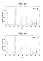
- Fig. 4(a) shows the X-ray diffraction pattern of sample No. 2.
- Fig. 4(b) shows the X-ray diffraction pattern of sample No. 7.
- the ordinate axis represents the X-ray diffraction intensity, which is a relative value when the maximum value is normalized as 1.
- the abscissa axis represents the diffraction angle. In No. 7, a peak was observed at a 2 ⁇ angle of 28.0° to 28.4°, and the precipitation of a BaMgSiO 4 crystal was demonstrated.
- Powders of barium carbonate, magnesium oxide, silicon dioxide, europium oxide, and manganese oxide were used.
- An ammonium chloride powder was used as a flux.
- the powers were each weighed so that the composition shown in Table 3 could be obtained.
- the powders were then mixed in a plastic pot. The mixture was dried and then calcined under the atmosphere at 1150°C for 3 hours. The mixture was then heat-treated by heating at 1250°C for 9 hours under a nitrogen gas flow containing 12% of hydrogen so that a phosphor was produced.
- Tables 3 and 4 show that in samples according to the invention, the precipitation of Ba 2 MgSi 2 O 7 , Ba 2 SiO 4 and BaMgSiO 4 crystals is suppressed so that the generation of green light is suppressed and that the red quantum efficiency is increased. It is also apparent that a quantum efficiency of 35% or more is obtained particularly in samples each with a D/(A+B+C+D) value of 0.04 to 0.26.
- Powders of barium carbonate, magnesium oxide, strontium carbonate, silicon dioxide, europium oxide, and manganese oxide were mixed so that the a, b and c values shown in Table 5 could be obtained for the compositional formula M 1 3-a Eu a Mg 1-b Mn b Si c O 8 .
- a predetermined amount of ammonium chloride was added as a flux.
- the materials were mixed in a plastic pot.
- the mixture was dried and then calcined under the atmosphere at the temperature shown in Table 5 for 3 hours.
- the mixture was then heat-treated by heating at the temperature shown in Table 5 for 9 hours under a nitrogen gas flow containing 12% of hydrogen (a reducing atmosphere) so that a phosphor according to the invention was prepared.
- sample No. 4 a combination of Ba and Sr was used as M 1 , the main crystal and the second phase were (Ba,Sr) 3 MgSi 2 O 8 and (Ba,Sr)MgSiO 4 , respectively.
- Fig. 2 shows a scanning electron microscopy (SEM) photograph (at a magnification of 1000x) of a phosphor according to the invention.
- SEM scanning electron microscopy
- the quantum efficiency of the resulting phosphor was measured using a spectrofluoro-photometer FP-6500 manufactured by JASCO Corporation.
- the phosphor powder was charged into a dedicated cell and irradiated with 395 nm exciting light when the fluorescence spectrum was measured.
- the red quantum efficiency was calculated from the result using the quantum efficiency measurement software included with the spectrofluoro-photometer. The result is shown in Table 6.
- the X-ray diffraction measurement of the phosphor was performed in the same manner as described above.
- A represents the X-ray diffraction peak intensity of the M 1 3 MgSi 2 O 8 crystal detected at a 2 ⁇ angle of about 31.5° to about 32°
- B represents the X-ray diffraction peak intensity of an M 1 2 MgSi 2 O 7 crystal detected at a 2 ⁇ angle of 27.7° to 28.2°
- C represents the X-ray diffraction peak intensity of an M 1 2 SiO 4 crystal detected at a 2 ⁇ angle of 29.2° to 29.8°
- D represents the X-ray diffraction peak intensity of an M 1 MgSiO 4 crystal detected at a 2 ⁇ angle of 28.0° to 28.4°.
- the positions of the detected peaks slightly shift to the high angle side from those in the case that M 1 is Ba.
- Samples within the scope of the invention are each composed substantially of the main Ba 3 MgSi 2 O 8 crystal and the second phase BaMgSiO 4 crystal and substantially free of M 1 2 MgSi 2 O 7 and M 1 2 SiO 4 crystals.
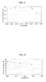
- Fig 5 shows the relationship between the peak intensity ratio D/(A+B+C+D) and the red quantum efficiency in the samples.
- Sample No. Chemical Composition M 1 element a a/c b b/c c calcining temperature (°C) heat-treating temperature in the reducing atmosphere (°C) 1 M 1 3-a Eu a Mg 1-b Mn b Si c O 8 Ba 0.075 0.039 0.075 0.039 1.905 1150 1250 2 M 1 3-a Eu a Mg 1-b Mn b Si c O 8 Ba 0.225 0.118 0.075 0.039 1.905 1150 1250 3 M 1 3-a Eu a Mg 1-b Mn b Si c O 8 Ba 0.264 0.139 0.075 0.039 1.905 1150 1250 4 M 1 3-a Eu a Mg 1-b Mn b Si c O 8 (Ba 0.75 Sr 0.25 ) 0.2 0.105 0.100 0.052 1.905 1150 1250 5 M 1 3-a Eu a
- the phosphor with a relative value of X-ray diffraction peak intensity outside the scope of the invention contains a large amount of the precipitated BaMgSiO 4 crystal and is found to have low red quantum efficiency.
- the inventors have made experiments on the quantum efficiency in the case that the Ba 3 MgSi 2 O 8 and BaMgSiO 4 crystal grains exist separately and in the case that the BaMgSiO 4 crystal grains exist in the Ba 3 MgSi 2 O 8 crystal grains.
- a BaMgSiO 4 crystal powder was added to a Ba 3 MgSi 2 O 8 powder, and the quantum efficiency of the mixture was determined.
- the result is shown in the graph of Fig. 6.
- Fig. 6 shows that an increase in the amount of the addition of the BaMgSiO 4 crystal powder to the Ba 3 MgSi 2 O 8 powder results in a reduction in quantum efficiency. It is therefore found that the presence of the BaMgSiO 4 crystal grains in the Ba 3 MgSi 2 O 8 crystal grains allows an improvement in quantum efficiency.
Applications Claiming Priority (5)
| Application Number | Priority Date | Filing Date | Title |
|---|---|---|---|
| JP2006348419 | 2006-12-25 | ||
| JP2007014530 | 2007-01-25 | ||
| JP2007078282 | 2007-03-26 | ||
| JP2007222984 | 2007-08-29 | ||
| PCT/JP2007/074739 WO2008078711A1 (ja) | 2006-12-25 | 2007-12-21 | 蛍光体およびその製法ならびに波長変換器、発光装置、照明装置 |
Publications (2)
| Publication Number | Publication Date |
|---|---|
| EP2116586A1 true EP2116586A1 (de) | 2009-11-11 |
| EP2116586A4 EP2116586A4 (de) | 2012-03-07 |
Family
ID=39562500
Family Applications (1)
| Application Number | Title | Priority Date | Filing Date |
|---|---|---|---|
| EP07851091A Withdrawn EP2116586A4 (de) | 2006-12-25 | 2007-12-21 | Fluoreszenzstoff, herstellungsverfahren dafür, wellenlängenkonvertierer, fluoreszenzvorrichtung sowie leuchtvorrichtung |
Country Status (4)
| Country | Link |
|---|---|
| US (1) | US20100214763A1 (de) |
| EP (1) | EP2116586A4 (de) |
| JP (1) | JP5137850B2 (de) |
| WO (1) | WO2008078711A1 (de) |
Cited By (1)
| Publication number | Priority date | Publication date | Assignee | Title |
|---|---|---|---|---|
| DE112013005555B4 (de) | 2012-11-20 | 2020-07-02 | Panasonic Intellectual Property Management Co., Ltd. | Leuchtstoff und Verwendung des Leuchtstoffs in einer Lichtemissionseinrichtung, einer Bildaufnahmevorrichtung, einer Flüssigkristall-Anzeigevorrichtung, einer Beleuchtungsvorrichtung und einem Fahrzeug |
Families Citing this family (9)
| Publication number | Priority date | Publication date | Assignee | Title |
|---|---|---|---|---|
| FR2846663B1 (fr) * | 2002-11-05 | 2006-08-11 | Rhodia Elect & Catalysis | Materiau transformant la lumiere, notamment pour parois de serres, comprenant comme additif un silicate de baryum et de magnesium |
| JP4949793B2 (ja) * | 2006-09-29 | 2012-06-13 | 京セラ株式会社 | 蛍光体及び波長変換器ならびに発光装置 |
| JP5330263B2 (ja) * | 2007-12-07 | 2013-10-30 | 株式会社東芝 | 蛍光体およびそれを用いたled発光装置 |
| CN102585804A (zh) * | 2011-12-26 | 2012-07-18 | 天津理工大学 | 蓝紫光芯片激发的660纳米红光荧光材料及喷雾生产法 |
| WO2014184992A1 (ja) | 2013-05-14 | 2014-11-20 | パナソニックIpマネジメント株式会社 | 蛍光体および当該蛍光体を用いた発光装置、ならびに当該発光装置を備える投影装置および車両 |
| US10125315B2 (en) * | 2015-04-27 | 2018-11-13 | Merck Patent Gmbh | Phosphors and phosphor-converted LEDs |
| JP6447557B2 (ja) * | 2016-03-24 | 2019-01-09 | 日亜化学工業株式会社 | 発光装置の製造方法 |
| TW202210605A (zh) * | 2020-09-14 | 2022-03-16 | 李崇華 | 白光發光二極體及包含其之背光模組與顯示裝置 |
| CN116904186A (zh) * | 2023-07-17 | 2023-10-20 | 松山湖材料实验室 | 绿色荧光材料及其制备方法、发光器件 |
Citations (2)
| Publication number | Priority date | Publication date | Assignee | Title |
|---|---|---|---|---|
| US3544482A (en) * | 1968-03-15 | 1970-12-01 | Sylvania Electric Prod | Europium and manganese activated alkaline earth silicate phosphors |
| WO2005112135A2 (fr) * | 2004-04-16 | 2005-11-24 | Rhodia Chimie | Diode electroluminescente emettant une lumiere blanche |
Family Cites Families (2)
| Publication number | Priority date | Publication date | Assignee | Title |
|---|---|---|---|---|
| JP4101468B2 (ja) | 2001-04-09 | 2008-06-18 | 豊田合成株式会社 | 発光装置の製造方法 |
| FR2846663B1 (fr) * | 2002-11-05 | 2006-08-11 | Rhodia Elect & Catalysis | Materiau transformant la lumiere, notamment pour parois de serres, comprenant comme additif un silicate de baryum et de magnesium |
-
2007
- 2007-12-21 EP EP07851091A patent/EP2116586A4/de not_active Withdrawn
- 2007-12-21 WO PCT/JP2007/074739 patent/WO2008078711A1/ja active Application Filing
- 2007-12-21 US US12/521,295 patent/US20100214763A1/en not_active Abandoned
- 2007-12-21 JP JP2008551095A patent/JP5137850B2/ja not_active Expired - Fee Related
Patent Citations (2)
| Publication number | Priority date | Publication date | Assignee | Title |
|---|---|---|---|---|
| US3544482A (en) * | 1968-03-15 | 1970-12-01 | Sylvania Electric Prod | Europium and manganese activated alkaline earth silicate phosphors |
| WO2005112135A2 (fr) * | 2004-04-16 | 2005-11-24 | Rhodia Chimie | Diode electroluminescente emettant une lumiere blanche |
Non-Patent Citations (2)
| Title |
|---|
| See also references of WO2008078711A1 * |
| THOMAS L. BARRY: "Equilibria and Eu2+ luminescence of subsolidus phases bounded by Ba3MgSi2O8, Sr3MgSi2O8 and Ca3MgSi2O8", J. ELECTROCHEM. SOC.: SOLID STATE SCIENCE, 1968, pages 733-738, XP002667845, * |
Cited By (1)
| Publication number | Priority date | Publication date | Assignee | Title |
|---|---|---|---|---|
| DE112013005555B4 (de) | 2012-11-20 | 2020-07-02 | Panasonic Intellectual Property Management Co., Ltd. | Leuchtstoff und Verwendung des Leuchtstoffs in einer Lichtemissionseinrichtung, einer Bildaufnahmevorrichtung, einer Flüssigkristall-Anzeigevorrichtung, einer Beleuchtungsvorrichtung und einem Fahrzeug |
Also Published As
| Publication number | Publication date |
|---|---|
| EP2116586A4 (de) | 2012-03-07 |
| WO2008078711A1 (ja) | 2008-07-03 |
| US20100214763A1 (en) | 2010-08-26 |
| JPWO2008078711A1 (ja) | 2010-04-22 |
| JP5137850B2 (ja) | 2013-02-06 |
Similar Documents
| Publication | Publication Date | Title |
|---|---|---|
| EP2116586A1 (de) | Fluoreszenzstoff, herstellungsverfahren dafür, wellenlängenkonvertierer, fluoreszenzvorrichtung sowie leuchtvorrichtung | |
| TWI391472B (zh) | 螢光體及其製法與使用它之發光裝置 | |
| KR101356367B1 (ko) | 표시 장치용 조명 장치 및 표시 장치 | |
| KR101120155B1 (ko) | 형광체, 형광체 시트 및 형광체의 제조방법 및 상기 형광체를 사용한 발광장치 | |
| EP2128219A1 (de) | Fluoreszenzstoff, herstellungsverfahren dafür sowie wellenlängenkonvertierer, leuchtdiode und beleuchtungsvorrichtung | |
| EP2428544A1 (de) | Rot-fluoreszierende Substanz in lichtemittierender Vorrichtung und lichtemittierende Vorrichtung damit | |
| JP2008538652A (ja) | セラミック発光コンバーターを含む照明システム | |
| JP6061331B2 (ja) | 蛍光体、その製造方法、発光装置および画像表示装置 | |
| JPWO2014017580A1 (ja) | 蛍光体、その製造方法、発光装置および画像表示装置 | |
| EP3992264A1 (de) | Fluoreszenzkörper, verfahren zu seiner herstellung und lichtemittierende vorrichtung damit | |
| WO2019188319A1 (ja) | 蛍光体及びそれを用いた発光装置 | |
| JP2010006850A (ja) | 波長変換器および発光装置ならびに照明装置 | |
| JP6057231B2 (ja) | 蛍光体、発光装置、画像表示装置、顔料および紫外線吸収剤 | |
| US20130214305A1 (en) | Red light-emitting fluorescent substance and light-emitting device employing the same | |
| US20120230010A1 (en) | Fluorescent substance and light-emitting device employing the same | |
| JP2010225960A (ja) | 発光装置および照明装置 | |
| JP4949793B2 (ja) | 蛍光体及び波長変換器ならびに発光装置 | |
| JP2017210529A (ja) | 蛍光体、その製造方法、発光装置、画像表示装置、顔料、および、紫外線吸収剤 | |
| JP2009280793A (ja) | 蛍光体および波長変換器ならびに発光装置、照明装置 | |
| JP5004616B2 (ja) | 蛍光体とその製造方法および波長変換器ならびに発光装置 | |
| JP2010199273A (ja) | 発光装置および照明装置 | |
| JP2009203264A (ja) | 蛍光体および波長変換器ならびに発光装置、照明装置 | |
| JP5036454B2 (ja) | 蛍光体粒子および波長変換器ならびに発光装置 | |
| JP2008208202A (ja) | 蛍光体および波長変換器ならびに発光装置 | |
| JP2009238887A (ja) | 波長変換器および発光装置ならびに照明装置 |
Legal Events
| Date | Code | Title | Description |
|---|---|---|---|
| PUAI | Public reference made under article 153(3) epc to a published international application that has entered the european phase |
Free format text: ORIGINAL CODE: 0009012 |
|
| 17P | Request for examination filed |
Effective date: 20090625 |
|
| AK | Designated contracting states |
Kind code of ref document: A1 Designated state(s): AT BE BG CH CY CZ DE DK EE ES FI FR GB GR HU IE IS IT LI LT LU LV MC MT NL PL PT RO SE SI SK TR |
|
| DAX | Request for extension of the european patent (deleted) | ||
| A4 | Supplementary search report drawn up and despatched |
Effective date: 20120208 |
|
| RIC1 | Information provided on ipc code assigned before grant |
Ipc: C09K 11/77 20060101ALI20120127BHEP Ipc: H01L 33/00 20100101ALI20120127BHEP Ipc: C09K 11/08 20060101ALI20120127BHEP Ipc: C09K 11/59 20060101AFI20120127BHEP |
|
| STAA | Information on the status of an ep patent application or granted ep patent |
Free format text: STATUS: THE APPLICATION IS DEEMED TO BE WITHDRAWN |
|
| 18D | Application deemed to be withdrawn |
Effective date: 20120911 |