EP2106015B1 - Stromversorgungsvorrichtung für elektrisch angetriebene Spritzgießmaschine und elektrisch angetriebene Spritzgießmaschine - Google Patents
Stromversorgungsvorrichtung für elektrisch angetriebene Spritzgießmaschine und elektrisch angetriebene Spritzgießmaschine Download PDFInfo
- Publication number
- EP2106015B1 EP2106015B1 EP09001413.5A EP09001413A EP2106015B1 EP 2106015 B1 EP2106015 B1 EP 2106015B1 EP 09001413 A EP09001413 A EP 09001413A EP 2106015 B1 EP2106015 B1 EP 2106015B1
- Authority
- EP
- European Patent Office
- Prior art keywords
- power
- circuit
- voltage
- injection molding
- current
- Prior art date
- Legal status (The legal status is an assumption and is not a legal conclusion. Google has not performed a legal analysis and makes no representation as to the accuracy of the status listed.)
- Active
Links
Images


Classifications
-
- H—ELECTRICITY
- H02—GENERATION; CONVERSION OR DISTRIBUTION OF ELECTRIC POWER
- H02M—APPARATUS FOR CONVERSION BETWEEN AC AND AC, BETWEEN AC AND DC, OR BETWEEN DC AND DC, AND FOR USE WITH MAINS OR SIMILAR POWER SUPPLY SYSTEMS; CONVERSION OF DC OR AC INPUT POWER INTO SURGE OUTPUT POWER; CONTROL OR REGULATION THEREOF
- H02M3/00—Conversion of DC power input into DC power output
- H02M3/02—Conversion of DC power input into DC power output without intermediate conversion into AC
- H02M3/04—Conversion of DC power input into DC power output without intermediate conversion into AC by static converters
- H02M3/10—Conversion of DC power input into DC power output without intermediate conversion into AC by static converters using discharge tubes with control electrode or semiconductor devices with control electrode
- H02M3/145—Conversion of DC power input into DC power output without intermediate conversion into AC by static converters using discharge tubes with control electrode or semiconductor devices with control electrode using devices of a triode or transistor type requiring continuous application of a control signal
- H02M3/155—Conversion of DC power input into DC power output without intermediate conversion into AC by static converters using discharge tubes with control electrode or semiconductor devices with control electrode using devices of a triode or transistor type requiring continuous application of a control signal using semiconductor devices only
- H02M3/156—Conversion of DC power input into DC power output without intermediate conversion into AC by static converters using discharge tubes with control electrode or semiconductor devices with control electrode using devices of a triode or transistor type requiring continuous application of a control signal using semiconductor devices only with automatic control of output voltage or current, e.g. switching regulators
- H02M3/158—Conversion of DC power input into DC power output without intermediate conversion into AC by static converters using discharge tubes with control electrode or semiconductor devices with control electrode using devices of a triode or transistor type requiring continuous application of a control signal using semiconductor devices only with automatic control of output voltage or current, e.g. switching regulators including plural semiconductor devices as final control devices for a single load
-
- B—PERFORMING OPERATIONS; TRANSPORTING
- B29—WORKING OF PLASTICS; WORKING OF SUBSTANCES IN A PLASTIC STATE IN GENERAL
- B29C—SHAPING OR JOINING OF PLASTICS; SHAPING OF MATERIAL IN A PLASTIC STATE, NOT OTHERWISE PROVIDED FOR; AFTER-TREATMENT OF THE SHAPED PRODUCTS, e.g. REPAIRING
- B29C45/00—Injection moulding, i.e. forcing the required volume of moulding material through a nozzle into a closed mould; Apparatus therefor
- B29C45/17—Component parts, details or accessories; Auxiliary operations
- B29C45/76—Measuring, controlling or regulating
- B29C45/7666—Measuring, controlling or regulating of power or energy, e.g. integral function of force
-
- H—ELECTRICITY
- H02—GENERATION; CONVERSION OR DISTRIBUTION OF ELECTRIC POWER
- H02M—APPARATUS FOR CONVERSION BETWEEN AC AND AC, BETWEEN AC AND DC, OR BETWEEN DC AND DC, AND FOR USE WITH MAINS OR SIMILAR POWER SUPPLY SYSTEMS; CONVERSION OF DC OR AC INPUT POWER INTO SURGE OUTPUT POWER; CONTROL OR REGULATION THEREOF
- H02M5/00—Conversion of AC power input into AC power output, e.g. for change of voltage, for change of frequency, for change of number of phases
- H02M5/40—Conversion of AC power input into AC power output, e.g. for change of voltage, for change of frequency, for change of number of phases with intermediate conversion into DC
- H02M5/42—Conversion of AC power input into AC power output, e.g. for change of voltage, for change of frequency, for change of number of phases with intermediate conversion into DC by static converters
- H02M5/44—Conversion of AC power input into AC power output, e.g. for change of voltage, for change of frequency, for change of number of phases with intermediate conversion into DC by static converters using discharge tubes or semiconductor devices to convert the intermediate DC into AC
- H02M5/453—Conversion of AC power input into AC power output, e.g. for change of voltage, for change of frequency, for change of number of phases with intermediate conversion into DC by static converters using discharge tubes or semiconductor devices to convert the intermediate DC into AC using devices of a triode or transistor type requiring continuous application of a control signal
- H02M5/458—Conversion of AC power input into AC power output, e.g. for change of voltage, for change of frequency, for change of number of phases with intermediate conversion into DC by static converters using discharge tubes or semiconductor devices to convert the intermediate DC into AC using devices of a triode or transistor type requiring continuous application of a control signal using semiconductor devices only
-
- B—PERFORMING OPERATIONS; TRANSPORTING
- B29—WORKING OF PLASTICS; WORKING OF SUBSTANCES IN A PLASTIC STATE IN GENERAL
- B29C—SHAPING OR JOINING OF PLASTICS; SHAPING OF MATERIAL IN A PLASTIC STATE, NOT OTHERWISE PROVIDED FOR; AFTER-TREATMENT OF THE SHAPED PRODUCTS, e.g. REPAIRING
- B29C45/00—Injection moulding, i.e. forcing the required volume of moulding material through a nozzle into a closed mould; Apparatus therefor
- B29C45/17—Component parts, details or accessories; Auxiliary operations
- B29C45/76—Measuring, controlling or regulating
- B29C45/7666—Measuring, controlling or regulating of power or energy, e.g. integral function of force
- B29C2045/7673—Recovering energy or power from drive motors
-
- Y—GENERAL TAGGING OF NEW TECHNOLOGICAL DEVELOPMENTS; GENERAL TAGGING OF CROSS-SECTIONAL TECHNOLOGIES SPANNING OVER SEVERAL SECTIONS OF THE IPC; TECHNICAL SUBJECTS COVERED BY FORMER USPC CROSS-REFERENCE ART COLLECTIONS [XRACs] AND DIGESTS
- Y02—TECHNOLOGIES OR APPLICATIONS FOR MITIGATION OR ADAPTATION AGAINST CLIMATE CHANGE
- Y02P—CLIMATE CHANGE MITIGATION TECHNOLOGIES IN THE PRODUCTION OR PROCESSING OF GOODS
- Y02P70/00—Climate change mitigation technologies in the production process for final industrial or consumer products
- Y02P70/10—Greenhouse gas [GHG] capture, material saving, heat recovery or other energy efficient measures, e.g. motor control, characterised by manufacturing processes, e.g. for rolling metal or metal working
Definitions
- the present invention relates to an electrically driven injection molding machine and a power supply device for an electrically driven injection molding machine for supplying electric power to servo motors for driving the constituent parts of the electrically driven injection molding machine such as a screw, a mold opening/closing device, a molded product ejecting device.
- an injection molding machine is configured by a pair of metal molds, a mold clamping device for mold-clamping these metal molds, an injection device for melting resin and injecting the resin within the metal molds etc.
- the injection device is configured by an injection cylinder and a screw and a plunger which are driven in the rotational direction and an axial direction within the injection cylinder etc.
- the mold clamping device, the screw etc. are respectively driven by servo motors provided independently.
- the injection molding process includes a measuring process for melting resin and accumulating the melted resin at the tip end portion within the cylinder, a mold clamping process for mold-clamping the metal molds, an injection process for injecting the melted resin within the metal molds thus mold-clamped, a pressure holding process for holding the pressure of the melted resin after the injection, a mold opening process for opening the metal molds, and a protruding process for protruding an ejector pin to take out a molded product from the metal molds etc.
- a measuring process for melting resin and accumulating the melted resin at the tip end portion within the cylinder a mold clamping process for mold-clamping the metal molds
- an injection process for injecting the melted resin within the metal molds thus mold-clamped
- a pressure holding process for holding the pressure of the melted resin after the injection
- a mold opening process for opening the metal molds
- a protruding process for protruding an ejector pin to take out a molded product
- a large servo motor of a high output is employed as the servo motor for driving the screw in the axial direction in the injection process .
- needs of a so-called super-high speed injection molding has been increased which is excellent in the transfer property and can form a molded product of a complicated and fine shape and also a molded product of a thin thickness with good or excellent transfer property.
- An injection molding machine capable of executing such the super-high speed injection molding requires a further high output power in the injection process and so requires the servo motor of a larger scale.
- the servo motor is driven by a three-phase AC voltage generated by a servo amplifier formed by an inverter circuit.
- the inverter circuit is supplied with a DC voltage.
- the DC voltage can be obtained by rectifying the three-phase AC voltage supplied from the power receiving equipment of a factory by using a conventionally well-known converter.
- a DC current supplied to the servo amplifier is required to be large.
- a three-phase AC power supply for supplying the three-phase AC voltage also requires a large current supply ability and so the power receiving equipment of a factory is required to have a relatively large power capacity. Further, since the fee structure of electric power differs depending on the maximum power to be contracted, the electricity bill becomes high when the power receiving equipment of a large power capacity is installed. In view of the requirement of the energy saving and cost reduction, a technique is demanded which can reduce the power capacity required for the power receiving equipment to thereby reduce the required electricity bill.
- Japan Institute of Invention and Innovation, Journal of Technical Disclosure No. 97-6523 describes a PWM converter which is an AC/DC converter applied to the injection molding machine and including a loop for controlling the voltage of the converter and a control loop for maintaining the sine wave of the current, whereby the voltage is stabilized and the voltage can be converted into a DC current of high quality.
- the AC/DC converter since the three-phase AC current supplied from the three-phase AC power supply is controlled so as to be shaped in a sine wave, a harmonic wave causing the reduction of a power factor can be suppressed and a DC current can be obtained based on the stable voltage, advantageously.
- the power factor is kept to a value near 1, an amount of a reactive power is small and so the power is not consumed wastefully. Further, since a kinetic energy accumulated in the driving portion of the injection molding machine is regenerated as electric energy and returned to the power supply side as electric power, the energy efficiency is high.
- the power factor can be kept to a value near 1 and an amount of a reactive power can be reduced, the maximum power required to be high in the injection process is not reduced and the electric power required in the respective processes is not smoothed.
- the power capacity of the power receiving equipment is determined by the time average of the power consumed by production machines and working machines etc. installed in a factory, that is, an average power. When the power capacity is determined in this manner, since a large power is consumed at the time of the injection process, a phenomenon that the voltage within the factory reduces, that is, a so-called voltage drop may arise and a breaker may be tripped.
- US 6,424,207 B1 discloses a power supply device for supplying electric power to a load, the power supply device comprising an AC/DC converter and a power accumulating device coupled to a DC circuit of the AC/DC converter; the power accumulating device comprises a power accumulating circuit and a control circuit; the power accumulating circuit comprises a first loop circuit and a second loop circuit; the first loop circuit comprises a coil, a first switch circuit and a capacitor coupled in series between the positive and the negative terminal of the DC circuit; the second loop circuit comprises the coil and a second switch circuit coupled in series between the positive and the negative terminal of the DC circuit; and the power accumulating device is configured to accumulate electric power supplied from the DC circuit in the capacitor.
- An object of the invention is to provide a power supply device for an electrically driven injection molding machine which can obviate the aforesaid problem of the related art and the electrically driven injection molding machine having such the power supply device.
- an object of the invention is to provide the power supply device of the electrically driven injection molding machine and the electrically driven injection molding machine which can reduce the maximum power supplied from the outside in a process such as an injection process requiring a high output, can smooth a required power in respective processes, can reduce a power capacity required in the power receiving equipment of a factory, can reduce a cost of equipments and further can reduce a required electricity bill.
- a power supply device for supplying a DC voltage to a servo amplifier of an injection molding machine is configured by an AC/DC converter and a power accumulating device.
- the power accumulating device is connected to a DC circuit side of the AC/DC converter and is configured to accumulate the power.
- the power accumulating device supply to the servo amplifier a DC voltage higher than the DC voltage generated from the AC/DC converter.
- the invention provides an injection molding machine including the power supply device.
- a power supply device of an electrically driven injection molding machine which supplies electric power to a servo motor for driving a member of an electrically driven injection molding machine
- the power supply device comprising: an AC/DC converter; and a power accumulating device, wherein: the AC/DC converter is configured to convert an AC voltage into a DC voltage and supply the DC voltage to a servo amplifier for driving the servo motor; and the power accumulating device is coupled to a DC circuit of the AC/DC converter, and is configured to accumulate electric power supplied from the DC circuit in a capacitor, and when accepting a predetermined output request, to supply a DC voltage to the DC circuit to thereby supply to the servo amplifier a DC voltage higher than the DC voltage generated from the AC/DC converter.
- the power accumulating device comprises a power accumulating circuit and a control circuit;
- the power accumulating circuit comprises a first loop circuit and a second loop circuit;
- the first loop circuit comprises a coil, a first switch circuit and a capacitor coupled in series between a positive terminal and a negative terminal;
- the second loop circuit comprises the coil and a second switch circuit coupled in series between the positive terminal and the negative terminal.
- the first switch circuit comprises a first diode and a first transistor coupled in parallel, the first diode being coupled so as to flow a current in a direction from the positive terminal toward the negative terminal, and the first transistor being coupled so as to flow a current in an opposite direction when being driven by a control signal from the control circuit; and the second switch circuit comprises a second diode and a second transistor coupled in parallel, the second diode being coupled so as to flow a current in a direction from the negative terminal toward the positive terminal, and the second transistor being coupled so as to flow a current in an opposite direction when being driven by the control signal from the control circuit.
- the power supply device further comprises: a current detection circuit for detecting a current flowing into the coil, wherein the control circuit controls an opening/closing operation of the first switch circuit and the second switch circuit so that the current flowing into the coil of the power accumulating circuit is within a predetermined limit value.
- the power supply device further comprises: a voltage detection circuit for detecting a DC voltage of the AC/DC converter, wherein the control circuit controls an opening/closing operation of the first switch circuit and the second switch circuit so that the DC voltage of the AC/DC converter becomes a predetermined voltage.
- the power supply device further comprises: a voltage detection circuit for detecting a voltage of the capacitor of the power accumulating device, wherein the control circuit controls an opening/closing operation of the first switch circuit and the second switch circuit so that the voltage of the capacitor becomes a predetermined voltage at a time of accumulating power into the power accumulating device.
- an electrically driven injection molding machine comprising the power supply device according to the first aspect.
- the electrically driven injection molding machine further comprises: a screw; a mold opening/closing device; a molded product ejecting device; and a plurality of servo motors configured to drive the screw, the mold opening/closing device, and the molded product ejecting device.
- the power supply device for the injection molding machine includes the AC/DC converter and the power accumulating device and is configured in a manner that the power accumulating device is coupled to the DC circuit of the AC/DC converter, and is configured to accumulate electric power supplied from the DC circuit, and when accepting the predetermined output request, to supply a DC current to the DC circuit of the AC/DC converter to thereby supply to the servo amplifier a DC voltage higher than the DC voltage generated from the AC/DC converter.
- the AC/DC converter is configured by a diode rectifying circuit well known in the related art, the DC voltage becomes larger than the peak value of the AC voltage and the DC current is not supplied from the AC/DC converter.
- the AC/DC converter is configured by a rectifying circuit such as a PWM converter well known in the related art, that is, in the case of having a function of boosting the voltage of the DC circuit by using the switching operation of the transistor to thereby increase the voltage of the DC circuit higher than the peak value of the AC voltage, the switching operation of the transistor of the AC/DC converter is stopped at the time of supplying the DC current from the accumulating circuit, whereby a power is not supplied from the AC side of the AC/DC converter like the diode rectifying circuit.
- a rectifying circuit such as a PWM converter well known in the related art
- a DC power of a high voltage can be supplied from the power accumulating device in place of the AC/DC converter.
- a power capacity required for the AC/DC converter can be made small and the maximum power supplied to the injection molding machine from the outside can also be reduced.
- a power can be accumulated in the power accumulating device during another process requiring a relatively small amount of power, a power can be smoothed in the entirety of the molding process and so the power capacity required for the power receiving equipment of a factory can be made small.
- the maximum power can be reduced, the electricity bill can be saved.
- the power accumulating circuit constituting the power accumulating device is configured by a capacitor, a coil, diodes and transistors etc., wherein electric charges accumulated in the capacitor can be taken out or charged as a current flowing into the coil by utilizing the switching operation of the diodes and the transistors.
- the charging/discharging property of the capacitor can be determined by controlling the current of the coil. That is, since it is possible to utilize an accumulated power which is not influenced by the internal resistor of the power accumulating capacitor, unique effects of the invention can be attained that a cheap capacitor can be used.
- the current flowing into the coil constituting the power accumulating circuit is limited, such phenomena can be prevented from occurring that an excessive current flows into the coil to break it or that the power accumulating capacitor and the capacitor of the AC/DC converter become failure or are damaged by an excessive charging/discharging current.
- the DC voltage supplied to the servo amplifier from the power accumulating device is controlled so as to be a predetermined voltage, the DC voltage supplied to the servo amplifier can be stabilized.
- the power accumulated in the power accumulating device is controlled so as to be a suitable voltage, an abnormal voltage is prevented from being applied to the power accumulating circuit.
- the power supply device for an electrically driven injection molding machine 100 also rectifies a three-phase AC current and supplies a DC voltage to a servo amplifier.
- the power supply device 1 for an electrically driven injection molding machine 100 according to the embodiment is also coupled to a three-phase AC power supply PW and the positive voltage line P on a DC circuit side thereof is coupled to servo amplifiers SA1, SA2, SA3 and SA4.
- the power supply device 1 can supply a DC voltage to the servo amplifiers SA1, SA2, SA3 and SA4 via a positive voltage line P.
- the servo amplifiers SA1, SA2, SA3 and SA4 can drive servo motors SM1, SM2, SM3 and SM4 provided in correspondence to an injection axis S1 for driving a screw in an axial direction, a plasticizing axis S2 for driving the screw in the rotation direction, a mold opening/closing axis S3 and an ejecting axis S4 for driving an ejector pin, respectively.
- the power supply device 1 is configured by an AC/DC converter 2 for converting the three-phase AC voltage into the DC voltage and a power accumulating device 3.
- the power accumulating device 3 stores a power supplied from the AC/DC converter 2 and is arranged to, when receiving an output request, control the stored power into a predetermined voltage and supply the voltage to the positive voltage line P.
- the AC/DC converter 2 is a converter for converting the three-phase AC voltage into the DC voltage and is configured by a diode rectifying circuit 201, a PWM converter 202, etc.
- the diode rectifying circuit 201 is configured by six diodes 11 to 16 and a capacitor 17 as shown in Fig. 1B .
- the diode rectifying circuit 201 is arranged in a manner that the polarities of all the diodes are aligned in the same direction, then three pairs of the diodes each pair including two diodes connected in series are disposed in parallel and connected between the positive DC voltage line and the negative DC voltage line, and three lines of the respective phases of the three-phase AC power supply are connected to the connection points between the two diodes of the three pairs respectively.
- the three-phase AC voltage is rectified by the diodes 11 to 16 and the DC voltage is supplied to the outside from a positive terminal P and a negative terminal N.
- the pulsating component of the DC voltage generated by the rectifying operation is smoothed by the capacitor 17 provided between the positive terminal P and the negative terminal N.
- the PWM converter 202 is configured by six transistors 21 to 26, six diodes 31 to 36 and a capacitor 37 as shown in Fig. 1C .
- the PWM converter 202 is a modified circuit of the diode rectifying circuit 201.
- the PWM converter 202 is arranged in a manner that the transistors 21 to 26 are respectively coupled in parallel to the diodes 31 to 36 which correspond to the respective diodes of the diode rectifying circuit 201, whereby a current can be flown in the direction opposite to the forward direction of each of the diodes 31 to 36 when the corresponding one of the transistors 21 to 26 is turned on, respectively.
- the PWM converter 202 can rectify and convert the three-phase AC current into the DC current like the diode rectifying circuit 201.
- the PWM converter 202 is configured to be substantially same as a well known inverter circuit, when the transistors 21 to 26 are controlled by a not-shown control circuit, a regenerative power collected from the DC current side can be returned to the three-phase AC power supply side like the well known technique of the related art.
- a power accumulating device 3 is configured by a power accumulating circuit 4 and a control circuit 5, as shown in Fig. 2A .
- the power accumulating circuit 4 stores power supplied form the AC/DC converter 2 via the positive terminal P and the negative terminal N of the DC voltage and outputs the stored power from the positive terminal P and the negative terminal N as the DC voltage.
- the control circuit 5 controls the power accumulating circuit 4.
- the power accumulating circuit 4 is coupled to the control circuit 5 via a photo coupler so as to be electrically insulated to each other in order to prevent such a phenomenon that the current on the power accumulating circuit 4 side flows into the control circuit 5 to thereby break the electronic element within the control circuit 5.
- the power accumulating circuit 4 and the control circuit 5 are shown in a directly coupled manner.
- the power accumulating circuit 4 is configured by the positive terminal P and the negative terminal N, a capacitor C, a coil L, and first and second switch circuits SW 1 , SW 2 .
- the first switch circuit SW 1 is configured by a first transistor Tr 1 and a first diode D 1
- the second switch circuit SW 2 is configured by a second transistor Tr 2 and a second diode D 2 .
- a coil current flowing through the coil L is measured by a current detector CT.
- An electric double layer capacitor is used as the capacitor C, for example.
- An insulated-gate bipolar transistor, that is, an IGBT is used as each of the transistors Tr 1 , Tr 2 .
- FIG. 2A is a power storage circuit according to the first embodiment and an equivalent circuit thereof is shown in Fig. 2B .
- the power accumulating circuit 4 will be explained with reference to the simplified drawing of Fig. 2B .
- the negative terminal N, the positive terminal P and the coil L connected to the positive terminal P are coupled by first and second loop circuits LP 1 , LP 2 .
- the first loop circuit LP 1 is a series circuit of the negative terminal N, the positive terminal P, the coil L, the first switch circuit SW 1 and the capacitor C.
- the second loop circuit LP 2 is a series circuit of the negative terminal N, the positive terminal P, the coil L and the second switch circuit SW 2 .
- Each of the switch circuits SW 1 , SW 2 is configured by a parallel circuit of a diode and a transistor, and is a circuit for controlling the flow of a current in a manner that a current is freely flown in one direction but a current is flown in the opposite direction only when the transistor is turned on, that is, when the transistor is switched to an ON state.
- the first diode D 1 is connected so as to flow the current from the positive terminal P to the negative terminal N, and the first transistor Tr 1 is coupled in parallel to the first diode D 1 so as to flow the current in the opposite direction when it is turned on.
- the second diode D 2 is connected so as to flow the current from the negative terminal N to the positive terminal P, and the second transistor Tr 2 is coupled in parallel to the second diode D 2 so as to flow the current in the opposite direction when it is turned on.
- a voltage between the negative and positive terminals N, P that is, a terminal voltage V FB1 is detected by a voltage detector VT 1 and applied to the control circuit 5 via a signal line S A .
- a voltage of power accumulated in the capacitor C that is, an accumulated voltage V FB2 is also detected by a voltage detector VT 2 and applied to the control circuit 5 via a signal line S B . Since the control circuit 5 is also connected to a signal line Sc from the current detector CT, a coil current I FB flowing through the coil L is also applied to the control circuit 5.
- control circuit 5 Since the control circuit 5 is connected to the first transistor Tr 1 via a signal line ST 1 and connected to the second transistor Tr 2 via a signal line ST 2 , the transistors Tr 1 , Tr 2 can be turned on and off by a control signal from the control circuit 5. The processing performed by the control circuit 5 will be explained in detail later.
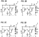
- the function of the power accumulating circuit 4 will be explained with reference to Figs. 3A to 3D .
- the first diode D 1 is disposed so as to flow the current freely from the positive terminal P to the capacitor C in the initial state
- the voltage on the positive electrode (+) side of the capacitor C is equal to the voltage of the positive terminal P.
- the accumulated voltage V FB2 is same as the terminal voltage V FB1 .
- the explanation will be made as to a case where electric power is accumulated from this state.
- the second transistor Tr 2 is switched, that is, turned on.
- a current flows as shown by an arrow Y A .
- the smoothing capacitor 17 or 37 is provided at the AC/DC converter 2 connected to the positive and negative terminals P, N.
- the terminal voltage V FB1 can be maintained at a stable predetermined voltage so that the electric charges of each of the smoothing capacitors 17, 37 becomes constant.
- the control circuit 5 controls the power accumulating circuit 4.
- the calculation function of the control circuit 5 is realized by two first and second functional blocks FB 1 , FB 2 .
- the first functional block FB 1 is a functional block for controlling and converting the power accumulated in the capacitor C into a predetermined voltage or a predetermined current to thereby output to the outside of the power accumulating device 3.
- the second functional block FB 2 is a functional block for accumulating the power supplied from the outside into the capacitor C.
- the setting value of the terminal voltage V FB1 that is, an output voltage setting value V SET1 is given from the outside.
- the output voltage setting value V SET1 and the measured terminal voltage V FB1 are input to a first adding point KA V1 to thereby calculate a voltage deviation value E V1 therebetween.
- the voltage deviation value E V1 is subjected to an operation amplification processing by a voltage controller K V1 , whereby a provisional setting current I SET1' to be flown into the coil L is obtained.
- the provisional setting current I SET1' is limited by a limiter L im1 so as not to exceed the limited value I LIM1 of the coil current applied from the outside to thereby obtain a current setting value I SET1 .
- the current setting value I SET1 and a measured coil current I FB are input to a second adding point KA C1 to thereby calculate a current deviation value E C1 therebetween.
- the polarity of each of the current setting value I SET1 and the coil current I FB is set to be positive in the direction of the current flowing from the coil L toward the terminal P.
- the current deviation value E C1 is subjected to an operation amplification processing by a current controller K C1 , and the output of the current controller is modulated in the pulse width of an ON time or OFF time thereof by a pulse width modulator PWM 1 in a manner that a ratio of the ON time of the first transistor T r1 becomes larger as the output of the current controller K C1 becomes larger.
- the output of the pulse width modulator is inputted to an AND element AND 1 .
- the output of the pulse width modulator is logically multiplied by a signal of a signal line S 1 described later by the AND element AND 1 and the output signal of the AND element is outputted from a signal line S T1 .
- the voltage between the terminals P and N can be set to the output voltage setting value V SET1 by turning on and off the first transistor T r1 , and the power accumulated in the capacitor C can be outputted between the terminals P and N. Further, the coil current I FB in this case can also be controlled.
- the setting value of the accumulated voltage V FB2 that is, an accumulated voltage setting value V SET2 is given from the outside.
- the accumulated voltage setting value V SET2 and the measured accumulated voltage V FB2 are input to a third adding point KA V2 to thereby calculate a voltage deviation value E V2 therebetween.
- the voltage deviation value E V2 is subjected to an operation amplification processing by a voltage controller K V2 , whereby a provisional setting current I SET2' to be flown into the coil L is obtained.
- the provisional setting current I SET2' is limited by a limiter L im2 so as not to exceed the limited value I LIM2 of the coil current applied from the outside to thereby obtain a current setting value I SET2 .
- the current setting value I SET2 and the measured coil current I FB are input to a fourth adding point KA C2 to thereby calculate a current deviation value E C2 therebetween.
- the polarity of each of the current setting value I SET2 and the coil current I FB is set to be positive in the direction of the current flowing from the terminal P toward the coil L.
- the current deviation value E C2 is subjected to an operation amplification processing by a current controller K C2 , and the output of the current controller is modulated in the pulse width of an ON time or OFF time thereof by a pulse width modulator PWM 2 in a manner that a ratio of the ON time of the second transistor T r2 becomes larger as the output of the current controller K C2 becomes larger.
- the output of the pulse width modulator is inputted to an AND element AND 2 .
- the output of the pulse width modulator is logically multiplied by a signal of a signal line S 2 described later by the AND element AND 2 and the output signal of the AND element is outputted from a signal line S T2 .
- the voltage of the accumulated voltage V FB2 is controlled so as to coincide with the accumulated voltage setting value V SET2 applied from the outside while controlling the coil current I FB , whereby the capacitor C can accumulate a power of C ⁇ V SET2 2 /2.
- the control circuit 5 is also applied with a switching signal C MND from the outside via a signal line S CMD .
- the signal line S CMD is arranged in a manner that one branch thereof is coupled to the AND element AND 2 via the signal line S 2 and the other branch thereof is coupled to the AND element AND 1 via an inverter element INV and further the signal line S 1 .
- the switching signal C MND is formed by a binary value representing ON and OFF states, that is, a logical signal having high and low levels.
- the polarity of the signal applied to the signal line S 1 is inverted with respect to the polarity of the signal of the signal line S 2 by the action of the inverter element INV.
- the ON signal is not outputted simultaneously to both the signal lines S T1 and S T2 .
- both the transistors Tr 1 , Tr 2 are prevented from being turned on simultaneously.
- This embodiment is configured in a manner that the first transistor Tr 1 is turned on when the signal of the signal line S T1 is at the high level and turned off when the signal of the signal line S T1 is at the low level, whilst the second transistor Tr 2 is turned on when the signal of the signal line S T2 is at the high level and turned off when the signal of the signal line S T2 is at the low level.
- the switching signal C MND is made high, since the second transistor Tr 2 can be turned on, the power accumulating circuit 4 can accumulate power.
- the switching signal C MND is made low, since the first transistor Tr 1 can be turned on, the accumulated power can be outputted to the outside.
- Fig. 5A is a graph showing the power consumed in an injection process and a pressure maintaining process, that is, the consumption power of an injection power P I .
- a numeral 41 although the injection process requires a quite large electric power, an amount of the consumption electric power is not so large since the injection time period is quite short.
- a plasticizing process that is, the measurement of the melted resin is performed by rotating the screw within the injection cylinder of the injection device after completing the pressure maintaining process, as is well known in the related art.
- Fig. 5B shows an amount of the consumed power of the plasticizing power P R by a numeral 43. As is shown in this figure, the plasticizing process takes a relatively long time and a predetermined electric power is consumed. When the resin injected within the metal molds is cooled and solidified, the mold clamping device is operated to open the molds.
- FIG. 5C shows an amount of electric power consumed in the mold clamping device, that is, a mold opening/closing power P M .
- the electric power consumed in the mold opening process shown by a numeral 44 is a predetermined power and this process does not take a long time.
- An amount of electric power consumed in a protruding process for protruding a molded product after the mold opening process, that is, a protruding power P E shown in Fig. 5D is small as shown by a numeral 46 and a time required for this process is short.
- a mold closing process for closing the metal molds requires a predetermined amount of electric power as shown by a numeral 45 and a time required for this process is relatively short.
- the power accumulating device 3 supplies a large electric power instantaneously to a servo amplifier in place of the AC/DC converter 2 in the injection process requiring the largest power among the respective processes for the molding.
- the power accumulating device accumulates an electric power during a process(es) requiring a relatively small amount of electric power.
- An input/output power P BNK is shown by numerals 47 and 48 in Fig. 5E , wherein numeral 47 represents the power outputted to the outside from the power accumulating device 3, and numeral 48 represents the power supplied from the outside to the power accumulating device 3.
- a positive power represents a power outputted to the outside from the power accumulating device 3 and a negative power represents a power supplied to the device from the outside.
- a portion shown by a numeral 47 has the same shape as the graph shown by the numeral 41, and a portion shown by a numeral 48 is a small negative power. Since an amount of electric power to be outputted and an amount of electric power to be accumulated is same, an area surrounded by the graph shown by the numeral 47 and the time axis is same as an area surrounded by the graph shown by the numeral 48 and the time axis.
- An electric power supplied from the external three-phase AC power supply PW, that is, an input power P IN is obtained by subtracting an input/output power P BNK of the power accumulating device 3 from the sum of powers P I , P R , P M , P E required in the respective processes.
- Fig. 5F shows a graph of the input power P IN . Although the power necessary for the injection process is cut as shown by a numeral 41', a power required during a time period other than the injection process is not so large as shown by the numeral 49.
- T CYC T I1 + T I2 + T R + T M1 + T M2 + T E + T S
- T CYC represents the molding cycle time, T I1 the injection time, T I2 the pressure maintaining time, T R a measuring time, T M1 a mold opening time, T M2 a mold closing time, T E a protruding time, T S a downtime, T CH a charging time (a time period for accumulating a power), P I2 a power for pressure maintaining, PR a power for plasticizing (a power for measuring), P M1 a power for mold opening, P M2 a power for mold closing,
- the maximum power in the molding process can be reduced and the power consumed in the molding cycle can be smoothed.
- the power capacity of the power receiving equipment of a factory it is sufficient to merely take the average power P AVE into consideration and it is not necessary to take the maximum power into consideration.
- the power capacity of the power receiving equipment of a factory can be made small.
- Figs. 6A to 6D are graphs showing the changes of the input/output power P BNK , the coil current I FB flowing into the coil L and the accumulated voltage V FB2 of the capacitor C in the case where a power is inputted into and outputted from the power accumulating circuit 4.
- Fig. 6A shows a graph 51 representing a power P BNK_D outputted from the power accumulating circuit 4 to the outside and a graph 52 representing a power P BNK_C supplied from the outside and accumulated.
- the first transistor T r1 is turned on and off.
- a so-called a current continuous mode is set, whereby the coil current I FB flows continuously as shown by a numeral 53 in Fig. 6B .
- the second transistor T r2 is turned on and off.
- the coil current I FB flows continuously as shown by a numeral 54, like the case of outputting the power.
- the accumulated voltage V FB2 of the capacitor C reduces as shown by a graph represented by a numeral 55 when the power accumulating circuit 4 outputs a power to the outside, whilst increases as shown by a graph represented by a numeral 57 when a power is accumulated in the power accumulating circuit.
- a so-called current discontinuous mode is set in which the coil current I FB flows intermittently.
- Fig. 6D shows graphs represented by numerals 58 and 59 in the case of outputting and accumulating a power in the current discontinuous mode, respectively.
- Figs. 7A to C show power accumulating circuits 4a, 4b, 4c according to second, third and fourth embodiments, respectively.
- Each of the power accumulating circuits 4a, 4b and 4c according to the second, third and fourth embodiments is modified only in a part of the arrangement of the constituent element, that is, electronic parts of the power accumulating circuit 4 according to the first embodiment, and is common to the first embodiment in the electronic parts.
- the electronic parts identical to those of the first embodiment are referred to by the common symbols, with explanation thereof being omitted.
- the power accumulating circuit 4a according to the second embodiment is configured in a manner that the capacitor C and the first switch circuit SW 1 are exchanged in their arrangement in the power accumulating circuit 4 of the first embodiment.
- the power accumulating circuit 4b according to the third embodiment is configured in a manner that the coil L coupled to the positive terminal P in the power accumulating circuit 4 of the first embodiment is coupled to the terminal N.
- the power accumulating circuit 4c according to the fourth embodiment is configured in a manner that the positions of the capacitor C and the first switch circuit SW1 in the power accumulating circuit 4b of the third embodiment are exchanged.
- Fig. 8A shows a power accumulating device 3' including a power accumulating circuit 4d according an example outside the invention and Fig. 8B shows an equivalent circuit of the power accumulating circuit 4d.
- the constitutional parts that is, electronic parts which action and effects are identical to those of the power accumulating device 3 according to the first embodiment are referred to by the common symbols added with ', with explanation thereof being omitted.
- the power accumulating circuit 4d is same as the power accumulating circuits 4, 4a, 4b and 4c according to the first to fourth embodiments in a point that a power supplied from the outside is accumulated and the accumulated power is converted into a high voltage larger than the DC voltage supplied from the AC/DC converter 2 to thereby supply the high voltage to the outside, but differs in some points. That is, firstly, the voltage of the power accumulated in the capacitor C', that is, the accumulated voltage V FB2 does not exceed the terminal voltage V FB1 . Thus, in the power accumulating circuit 4d, a capacitor C' is not required to have an excessive withstanding voltage efficiency.
- the power accumulating circuit 4d differs from the power accumulating circuits 4, 4a, 4b and 4c according to the first to fourth embodiments also in the case of supplying the accumulated power to the outside. That is, when a first transistor T r1' is turned on, the power accumulated in the capacitor C' is input to the coil L' and the first transistor T r1' , whereby magnetic energy is accumulated in the coil L'. In this case, the power from the capacitor C' is not supplied to any of the positive and negative terminals P, N. When the first transistor T r1' is turned off, a voltage obtained by adding an electromotive force generated at the coil L' to the accumulated voltage V FB2 is input between the positive and negative terminals P, N. When the ON/OFF operation of the first transistor Tr1' is repeated, a predetermined power can be supplied between the positive and negative terminals P, N.
- each of the power accumulating circuits 4, 4a, 4b, 4c and 4d includes only one capacitor, a plurality of capacitors may be provided in series or in parallel in place of providing one capacitor. Further, it will be clear that the invention can be implemented even if a resistor is provided at an arbitrary position of each of the power accumulating circuits 4, 4a, 4b, 4c and 4d.
Landscapes
- Engineering & Computer Science (AREA)
- Power Engineering (AREA)
- Manufacturing & Machinery (AREA)
- Mechanical Engineering (AREA)
- Injection Moulding Of Plastics Or The Like (AREA)
Claims (7)
- Leistungsversorgungseinrichtung einer elektrisch angetriebenen Spritzgießanlage zum Zuführen elektrischer Leistung zu einem Servomotor (SM1; SM2; SM3; SM4) zum Antreiben eines Elements der elektrisch angetriebenen Spritzgießanlage, wobei die Leistungsversorgungseinrichtung aufweist:einen Wechselstrom/Gleichstrom-Wandler (2); undeine Leistungsakkumulationseinrichtung (3), wobei:der Wechselstrom/Gleichstrom-Wandler (2) ausgebildet ist, eine Wechselstromspannung in eine Gleichstromspannung umzuwandeln, die einem Servoverstärker (SA1; SA2; SA3; SA4) zum Ansteuern des Servomotors (SM1; SM2; SM3; SM4) zugeführt werden kann;die Leistungsakkumulationseinrichtung (3) mit einer Gleichstromschaltung des Wechselstrom/Gleichstrom-Wandlers (2) verbunden ist;die Leistungsakkumulationseinrichtung (3) eine Leistungsakkumulationsschaltung (4) und eine Steuerschaltung (5) aufweist;die Leistungsakkumulationsschaltung (4) eine erste Schleifenschaltung und eine zweite Schleifenschaltung aufweist;die erste Schleifenschaltung eine Spule (L), eine erste Schaltschaltung (SW1) und einen Kondensator (C), die in Reihe zwischen einem positiven Anschluss (P) und einem negativen Anschluss (N) geschaltet sind, aufweist;die zweite Schleifenschaltung die Spule (L) und eine zweite Schaltschaltung (SW2) aufweist, die zwischen dem positiven Anschluss (P) und dem negativen Anschluss (N) in Reihe geschaltet sind;die Leistungsakkumulationseinrichtung (3) ausgebildet ist, elektrische Leistung, die von der Gleichstromschaltung geliefert wird, in dem Kondensator (C) zu speichern, und bei Empfang einer vorbestimmten Ausgabeanforderung bezüglich einer Gleichstromspannung zum Antreiben des Elements der elektrisch angetriebenen Spritzgießanlage die Gleichstromspannung der Gleichstromschaltung zuzuführen, um damit den Servoverstärker (SA1; SA2; SA3; SA4) mit einer Gleichstromspannung zu versorgen, die höher ist als die Gleichstromspannung, die von dem Wechselstrom/Gleichstrom-Wandler (2) erzeugt wird.
- Leistungsversorgungseinrichtung einer elektrisch angetriebenen Spritzgießanlage nach Anspruch 1, wobei:die erste Schaltschaltung (SW1) eine erste Diode (D1) und einen ersten Transistor (Tr1), die parallel geschaltet sind, aufweist, wobei die erste Diode (D1) so angeschlossen ist, dass ein Strom in einer Richtung von dem positiven Anschluss (P) zu dem negativen Anschluss (N) fließt, und wobei der erste Transistor (Tr1) so angeschlossen ist, dass ein Strom in einer umgekehrten Richtung fließt, wenn eine Ansteuerung durch ein Steuersignal aus der Steuerschaltung (5) erfolgt; unddie zweite Schaltschaltung (SW2) eine zweite Diode (D2) und einen zweiten Transistor (Tr2), die parallel geschaltet sind, aufweist, wobei die zweite Diode (D2) so angeschlossen ist, dass ein Strom in einer Richtung von dem negativen Anschluss (N) zu dem positiven Anschluss (P) fließt, und wobei der zweite Transistor (Tr2) so angeschlossen ist, dass ein Strom in umgekehrter Richtung fließt, wenn eine Ansteuerung durch das Steuersignal aus der Steuerschaltung (5) erfolgt.
- Leistungsversorgungseinrichtung einer elektrisch angetriebenen Spritzgießanlage nach Anspruch 2, die ferner aufweist:eine Stromdetektionsschaltung (CT; SC) zum Erfassen eines Stroms, der in der Spule (I) fließt,wobei die Steuerschaltung (5) einen Öffnungs/Schließvorgang der ersten Schaltschaltung (SW1) und der zweiten Schaltschaltung (SW2) derart steuert, dass der in die Spule (L) der Leistungsakkumulationsschaltung (4) fließende Strom innerhalb eines vorbestimmten Grenzwertes liegt.
- Leistungsversorgungseinrichtung einer elektrisch angetriebenen Spritzgießanlage nach Anspruch 1, die ferner aufweist:eine Spannungsdetektionsschaltung (VT1; SA) zum Erfassen einer Gleichstromspannung des Wechselstrom/Gleichstrom-Wandlers (2),wobei die Steuerschaltung (5) einen Öffnungs/Schließvorgang der ersten Schaltschaltung (SW1) und der zweiten Schaltschaltung (SW2) derart steuert, dass die durch die Leistungsakkumulationsschaltung (4) erzeugte Gleichstromspannung einen vorbestimmten Wert annimmt.
- Leistungsversorgungseinrichtung einer elektrisch angetriebenen Spritzgießanlage nach Anspruch 1, die ferner aufweist:eine Spannungsdetektionsschaltung (VT2; SB) zum Erfassen einer Spannung des Kondensators (C) der Leistungsakkumulationseinrichtung (3),wobei die Steuerschaltung einen Öffnungs/Schließvorgang der ersten Schaltschaltung (SW1) und der zweiten Schaltschaltung (SW2) derart steuert, dass die Spannung des Kondensators (C) eine vorbestimmte Spannung in der Zeit des Akkumulierens von Leistung in der Leistungsakkumulationseinrichtung (3) annimmt.
- Elektrisch angetriebene Spritzgießanlage, die eine Leistungsversorgungseinrichtung nach Anspruch 1 aufweist.
- Elektrisch angetriebene Spritzgießanlage nach Anspruch 6, die ferner aufweist:eine Schnecke;eine Formöffnungs/schließeinrichtung;eine Einrichtung zum Auswerfen eines hergestellten Produkts; undmehrere Servomotoren, die ausgebildet sind, die Schnecke, die Formöffnungs/schließeinrichtung und die Einrichtung zum Auswerfen eines hergestellten Produkts anzutreiben.
Applications Claiming Priority (1)
| Application Number | Priority Date | Filing Date | Title |
|---|---|---|---|
| JP2008087938A JP4756559B2 (ja) | 2008-03-28 | 2008-03-28 | 電動射出成形機の電力供給装置および電動射出成形機 |
Publications (3)
| Publication Number | Publication Date |
|---|---|
| EP2106015A2 EP2106015A2 (de) | 2009-09-30 |
| EP2106015A3 EP2106015A3 (de) | 2010-10-27 |
| EP2106015B1 true EP2106015B1 (de) | 2020-05-13 |
Family
ID=40875098
Family Applications (1)
| Application Number | Title | Priority Date | Filing Date |
|---|---|---|---|
| EP09001413.5A Active EP2106015B1 (de) | 2008-03-28 | 2009-02-02 | Stromversorgungsvorrichtung für elektrisch angetriebene Spritzgießmaschine und elektrisch angetriebene Spritzgießmaschine |
Country Status (3)
| Country | Link |
|---|---|
| US (1) | US8235693B2 (de) |
| EP (1) | EP2106015B1 (de) |
| JP (1) | JP4756559B2 (de) |
Families Citing this family (20)
| Publication number | Priority date | Publication date | Assignee | Title |
|---|---|---|---|---|
| JP5086396B2 (ja) | 2010-07-06 | 2012-11-28 | 株式会社日本製鋼所 | 電動射出成形機の電力供給方法 |
| JP5647068B2 (ja) * | 2011-05-13 | 2014-12-24 | 住友重機械工業株式会社 | 射出成形機 |
| JP5755522B2 (ja) * | 2011-07-08 | 2015-07-29 | 株式会社日本製鋼所 | 電動射出成形機およびその電力貯蔵装置 |
| JP5762869B2 (ja) * | 2011-07-26 | 2015-08-12 | 住友重機械工業株式会社 | 射出成形機 |
| JP5801128B2 (ja) * | 2011-07-26 | 2015-10-28 | 住友重機械工業株式会社 | 射出成形機 |
| JP5917365B2 (ja) * | 2011-12-28 | 2016-05-11 | 住友重機械工業株式会社 | 射出成形機 |
| JP5855475B2 (ja) * | 2012-01-26 | 2016-02-09 | 住友重機械工業株式会社 | 射出成形機システム及び射出成形機、並びに配電装置 |
| JP5868778B2 (ja) * | 2012-05-18 | 2016-02-24 | 住友重機械工業株式会社 | 射出成形機及び電源回生装置 |
| JP5680600B2 (ja) * | 2012-09-07 | 2015-03-04 | 株式会社日本製鋼所 | 電動射出成形機の直流電圧供給回路 |
| JP5570581B2 (ja) * | 2012-11-30 | 2014-08-13 | ファナック株式会社 | 電動射出成形機のモータ動力遮断装置 |
| JP6198596B2 (ja) * | 2013-12-11 | 2017-09-20 | 株式会社松井製作所 | 媒体供給装置 |
| JP5800938B2 (ja) * | 2014-03-19 | 2015-10-28 | ファナック株式会社 | 電源コンバータ制御部を有する射出成形機の制御装置 |
| JP6100292B2 (ja) * | 2015-01-26 | 2017-03-22 | 株式会社日本製鋼所 | 電動射出成形機の電力供給装置の制御方法および電力供給装置 |
| JP6377097B2 (ja) * | 2016-04-14 | 2018-08-22 | 株式会社日本製鋼所 | 射出成形機システム |
| JP6381572B2 (ja) * | 2016-04-15 | 2018-08-29 | 株式会社日本製鋼所 | 外部に電力供給が可能な電動射出成形機 |
| JP6576317B2 (ja) * | 2016-09-28 | 2019-09-18 | 株式会社日本製鋼所 | 電動射出成形機システム |
| JP7766414B2 (ja) * | 2021-05-31 | 2025-11-10 | 株式会社日本製鋼所 | 射出成形機 |
| JP2023160341A (ja) * | 2022-04-22 | 2023-11-02 | 株式会社日本製鋼所 | 電源装置およびそれを備えた射出成形機システム、ならびに、射出成形機に駆動電力を供給する方法およびプログラム |
| JP2024005064A (ja) * | 2022-06-29 | 2024-01-17 | 株式会社日本製鋼所 | 電源装置およびそれを備えた射出成形機システム、ならびに、射出成形機に駆動電力を供給する方法 |
| WO2024195682A1 (ja) * | 2023-03-22 | 2024-09-26 | 株式会社Nttドコモ | 消費電力最適化装置 |
Citations (1)
| Publication number | Priority date | Publication date | Assignee | Title |
|---|---|---|---|---|
| US6424207B1 (en) * | 2001-04-18 | 2002-07-23 | Northrop Grumman Corporation | PWM active filter for DC power systems |
Family Cites Families (13)
| Publication number | Priority date | Publication date | Assignee | Title |
|---|---|---|---|---|
| JPS61230917A (ja) * | 1985-04-08 | 1986-10-15 | Fanuc Ltd | 射出成形機の射出圧制御方式 |
| US5362222A (en) * | 1993-08-31 | 1994-11-08 | Cincinnati Milacron Inc. | Injection molding machine having a vector controlled AC drive system |
| JPH10174477A (ja) * | 1996-12-06 | 1998-06-26 | Hitachi Ltd | 電動機駆動装置及びこれを用いた空気調和機 |
| JPH1128751A (ja) * | 1997-07-09 | 1999-02-02 | Niigata Eng Co Ltd | 射出成形機の駆動制御装置 |
| JP3708728B2 (ja) * | 1998-11-05 | 2005-10-19 | 日創電機株式会社 | 射出成形機のモータ駆動装置 |
| JP4249364B2 (ja) * | 2000-02-28 | 2009-04-02 | 三菱電機株式会社 | エレベータの制御装置 |
| JP2002166456A (ja) * | 2000-12-04 | 2002-06-11 | Tokimec Inc | 横型成形機 |
| US6682332B2 (en) * | 2001-08-14 | 2004-01-27 | Alcoa Inc. | Dual isolated mode controller for injection molding machine |
| TWI221806B (en) * | 2001-10-19 | 2004-10-11 | Sumitomo Heavy Industries | Injection molding machine and method of protecting the injection molding machine |
| JP3722810B2 (ja) * | 2003-06-06 | 2005-11-30 | ファナック株式会社 | モータ駆動装置 |
| JP4830412B2 (ja) * | 2005-09-09 | 2011-12-07 | パナソニック株式会社 | 洗濯乾燥機 |
| JP4652224B2 (ja) * | 2005-12-20 | 2011-03-16 | 株式会社日本製鋼所 | 電動射出成形機のサーボ電源装置及び電動射出成形機のサーボ電源装置の制御方法 |
| JP2008087938A (ja) | 2006-10-04 | 2008-04-17 | Fuji Xerox Co Ltd | シート供給装置及び画像形成装置 |
-
2008
- 2008-03-28 JP JP2008087938A patent/JP4756559B2/ja active Active
-
2009
- 2009-02-02 EP EP09001413.5A patent/EP2106015B1/de active Active
- 2009-02-09 US US12/367,843 patent/US8235693B2/en not_active Expired - Fee Related
Patent Citations (1)
| Publication number | Priority date | Publication date | Assignee | Title |
|---|---|---|---|---|
| US6424207B1 (en) * | 2001-04-18 | 2002-07-23 | Northrop Grumman Corporation | PWM active filter for DC power systems |
Also Published As
| Publication number | Publication date |
|---|---|
| US8235693B2 (en) | 2012-08-07 |
| EP2106015A3 (de) | 2010-10-27 |
| US20090246307A1 (en) | 2009-10-01 |
| JP4756559B2 (ja) | 2011-08-24 |
| EP2106015A2 (de) | 2009-09-30 |
| JP2009241287A (ja) | 2009-10-22 |
Similar Documents
| Publication | Publication Date | Title |
|---|---|---|
| EP2106015B1 (de) | Stromversorgungsvorrichtung für elektrisch angetriebene Spritzgießmaschine und elektrisch angetriebene Spritzgießmaschine | |
| US8536833B2 (en) | Power supplying apparatus | |
| JP4512145B2 (ja) | モータ制御装置 | |
| JP5762617B2 (ja) | Dc/dcコンバータ | |
| EP2664053B1 (de) | Verfahren und vorrichtung zur bereitstellung einer unterbrechungsfreien stromversorgung | |
| US20120020126A1 (en) | Control device of transformer coupling type booster | |
| JP5755522B2 (ja) | 電動射出成形機およびその電力貯蔵装置 | |
| US9343986B2 (en) | Power converter with current feedback loop | |
| EP2416478A2 (de) | Elektromotorische Spritzgussmaschine und Stromversorgungsverfahren für elektromotorische Spritzgussmaschine | |
| US20160190971A1 (en) | Motor controller | |
| JPWO2018193606A1 (ja) | 電力変換装置 | |
| JP2010110936A (ja) | 電動射出成形機の電力表示方法および電力表示装置 | |
| CN104115389A (zh) | 功率转换装置 | |
| EP2647482B1 (de) | Spritzgussmaschine mit externer Vorrichtung, z.B. mit einem Leistungsverteiler | |
| JPWO2003103126A1 (ja) | 電力変換装置 | |
| JP6366647B2 (ja) | 蓄電装置を備えた電動射出成形機 | |
| JP2017217836A (ja) | 電力貯蔵装置を備えた電動射出成形機 | |
| CN105024537A (zh) | 启动再生式转换器的方法和再生式转换器 | |
| JP2016137577A (ja) | 電動射出成形機の電力供給装置の制御方法および電力供給装置 | |
| JP4870129B2 (ja) | 電動射出成形機の電力供給装置および電動射出成形機 | |
| JP5680600B2 (ja) | 電動射出成形機の直流電圧供給回路 | |
| JP6377097B2 (ja) | 射出成形機システム | |
| JP2012115018A (ja) | 電力制御装置 | |
| JP2007195352A (ja) | 電動機の電源装置 | |
| JP2010193590A (ja) | 電源瞬断対策回路、スイッチング電源装置、及び、コンデンサ充電制御方法 |
Legal Events
| Date | Code | Title | Description |
|---|---|---|---|
| PUAI | Public reference made under article 153(3) epc to a published international application that has entered the european phase |
Free format text: ORIGINAL CODE: 0009012 |
|
| AK | Designated contracting states |
Kind code of ref document: A2 Designated state(s): AT BE BG CH CY CZ DE DK EE ES FI FR GB GR HR HU IE IS IT LI LT LU LV MC MK MT NL NO PL PT RO SE SI SK TR |
|
| AX | Request for extension of the european patent |
Extension state: AL BA RS |
|
| PUAL | Search report despatched |
Free format text: ORIGINAL CODE: 0009013 |
|
| AK | Designated contracting states |
Kind code of ref document: A3 Designated state(s): AT BE BG CH CY CZ DE DK EE ES FI FR GB GR HR HU IE IS IT LI LT LU LV MC MK MT NL NO PL PT RO SE SI SK TR |
|
| AX | Request for extension of the european patent |
Extension state: AL BA RS |
|
| RIC1 | Information provided on ipc code assigned before grant |
Ipc: H02M 3/158 20060101AFI20090728BHEP Ipc: H02M 5/458 20060101ALI20100921BHEP |
|
| 17P | Request for examination filed |
Effective date: 20110427 |
|
| AKX | Designation fees paid |
Designated state(s): DE |
|
| STAA | Information on the status of an ep patent application or granted ep patent |
Free format text: STATUS: EXAMINATION IS IN PROGRESS |
|
| 17Q | First examination report despatched |
Effective date: 20180417 |
|
| GRAP | Despatch of communication of intention to grant a patent |
Free format text: ORIGINAL CODE: EPIDOSNIGR1 |
|
| STAA | Information on the status of an ep patent application or granted ep patent |
Free format text: STATUS: GRANT OF PATENT IS INTENDED |
|
| INTG | Intention to grant announced |
Effective date: 20200107 |
|
| RAP1 | Party data changed (applicant data changed or rights of an application transferred) |
Owner name: THE JAPAN STEEL WORKS, LTD. |
|
| RIN1 | Information on inventor provided before grant (corrected) |
Inventor name: OCHI, KIYOSHI |
|
| GRAS | Grant fee paid |
Free format text: ORIGINAL CODE: EPIDOSNIGR3 |
|
| GRAA | (expected) grant |
Free format text: ORIGINAL CODE: 0009210 |
|
| STAA | Information on the status of an ep patent application or granted ep patent |
Free format text: STATUS: THE PATENT HAS BEEN GRANTED |
|
| AK | Designated contracting states |
Kind code of ref document: B1 Designated state(s): DE |
|
| REG | Reference to a national code |
Ref country code: DE Ref legal event code: R096 Ref document number: 602009062018 Country of ref document: DE |
|
| REG | Reference to a national code |
Ref country code: DE Ref legal event code: R097 Ref document number: 602009062018 Country of ref document: DE |
|
| PLBE | No opposition filed within time limit |
Free format text: ORIGINAL CODE: 0009261 |
|
| STAA | Information on the status of an ep patent application or granted ep patent |
Free format text: STATUS: NO OPPOSITION FILED WITHIN TIME LIMIT |
|
| 26N | No opposition filed |
Effective date: 20210216 |
|
| PGFP | Annual fee paid to national office [announced via postgrant information from national office to epo] |
Ref country code: DE Payment date: 20241231 Year of fee payment: 17 |