EP2101363B1 - Semiconductor light-emitting element and method for producing the same - Google Patents
Semiconductor light-emitting element and method for producing the same Download PDFInfo
- Publication number
- EP2101363B1 EP2101363B1 EP09250663.3A EP09250663A EP2101363B1 EP 2101363 B1 EP2101363 B1 EP 2101363B1 EP 09250663 A EP09250663 A EP 09250663A EP 2101363 B1 EP2101363 B1 EP 2101363B1
- Authority
- EP
- European Patent Office
- Prior art keywords
- electrode
- semiconductor layer
- light
- void
- face
- Prior art date
- Legal status (The legal status is an assumption and is not a legal conclusion. Google has not performed a legal analysis and makes no representation as to the accuracy of the status listed.)
- Active
Links
Images


Classifications
-
- H—ELECTRICITY
- H10—SEMICONDUCTOR DEVICES; ELECTRIC SOLID-STATE DEVICES NOT OTHERWISE PROVIDED FOR
- H10H—INORGANIC LIGHT-EMITTING SEMICONDUCTOR DEVICES HAVING POTENTIAL BARRIERS
- H10H20/00—Individual inorganic light-emitting semiconductor devices having potential barriers, e.g. light-emitting diodes [LED]
- H10H20/80—Constructional details
- H10H20/83—Electrodes
- H10H20/831—Electrodes characterised by their shape
-
- H—ELECTRICITY
- H10—SEMICONDUCTOR DEVICES; ELECTRIC SOLID-STATE DEVICES NOT OTHERWISE PROVIDED FOR
- H10H—INORGANIC LIGHT-EMITTING SEMICONDUCTOR DEVICES HAVING POTENTIAL BARRIERS
- H10H20/00—Individual inorganic light-emitting semiconductor devices having potential barriers, e.g. light-emitting diodes [LED]
- H10H20/80—Constructional details
- H10H20/81—Bodies
- H10H20/822—Materials of the light-emitting regions
- H10H20/824—Materials of the light-emitting regions comprising only Group III-V materials, e.g. GaP
- H10H20/825—Materials of the light-emitting regions comprising only Group III-V materials, e.g. GaP containing nitrogen, e.g. GaN
-
- H—ELECTRICITY
- H10—SEMICONDUCTOR DEVICES; ELECTRIC SOLID-STATE DEVICES NOT OTHERWISE PROVIDED FOR
- H10H—INORGANIC LIGHT-EMITTING SEMICONDUCTOR DEVICES HAVING POTENTIAL BARRIERS
- H10H20/00—Individual inorganic light-emitting semiconductor devices having potential barriers, e.g. light-emitting diodes [LED]
- H10H20/80—Constructional details
- H10H20/83—Electrodes
- H10H20/832—Electrodes characterised by their material
- H10H20/833—Transparent materials
-
- H—ELECTRICITY
- H10—SEMICONDUCTOR DEVICES; ELECTRIC SOLID-STATE DEVICES NOT OTHERWISE PROVIDED FOR
- H10H—INORGANIC LIGHT-EMITTING SEMICONDUCTOR DEVICES HAVING POTENTIAL BARRIERS
- H10H20/00—Individual inorganic light-emitting semiconductor devices having potential barriers, e.g. light-emitting diodes [LED]
- H10H20/01—Manufacture or treatment
- H10H20/032—Manufacture or treatment of electrodes
-
- H—ELECTRICITY
- H10—SEMICONDUCTOR DEVICES; ELECTRIC SOLID-STATE DEVICES NOT OTHERWISE PROVIDED FOR
- H10H—INORGANIC LIGHT-EMITTING SEMICONDUCTOR DEVICES HAVING POTENTIAL BARRIERS
- H10H20/00—Individual inorganic light-emitting semiconductor devices having potential barriers, e.g. light-emitting diodes [LED]
- H10H20/80—Constructional details
- H10H20/83—Electrodes
- H10H20/831—Electrodes characterised by their shape
- H10H20/8316—Multi-layer electrodes comprising at least one discontinuous layer
-
- H—ELECTRICITY
- H10—SEMICONDUCTOR DEVICES; ELECTRIC SOLID-STATE DEVICES NOT OTHERWISE PROVIDED FOR
- H10W—GENERIC PACKAGES, INTERCONNECTIONS, CONNECTORS OR OTHER CONSTRUCTIONAL DETAILS OF DEVICES COVERED BY CLASS H10
- H10W72/00—Interconnections or connectors in packages
- H10W72/20—Bump connectors, e.g. solder bumps or copper pillars; Dummy bumps; Thermal bumps
-
- H—ELECTRICITY
- H10—SEMICONDUCTOR DEVICES; ELECTRIC SOLID-STATE DEVICES NOT OTHERWISE PROVIDED FOR
- H10W—GENERIC PACKAGES, INTERCONNECTIONS, CONNECTORS OR OTHER CONSTRUCTIONAL DETAILS OF DEVICES COVERED BY CLASS H10
- H10W72/00—Interconnections or connectors in packages
- H10W72/851—Dispositions of multiple connectors or interconnections
- H10W72/874—On different surfaces
- H10W72/884—Die-attach connectors and bond wires
-
- H—ELECTRICITY
- H10—SEMICONDUCTOR DEVICES; ELECTRIC SOLID-STATE DEVICES NOT OTHERWISE PROVIDED FOR
- H10W—GENERIC PACKAGES, INTERCONNECTIONS, CONNECTORS OR OTHER CONSTRUCTIONAL DETAILS OF DEVICES COVERED BY CLASS H10
- H10W72/00—Interconnections or connectors in packages
- H10W72/90—Bond pads, in general
- H10W72/941—Dispositions of bond pads
- H10W72/9415—Dispositions of bond pads relative to the surface, e.g. recessed, protruding
Definitions
- This invention relates to a semiconductor light-emitting element and a method for producing the same.
- a semiconductor light-emitting element For improving brightness of a semiconductor light-emitting element, improvement of light taking-out efficiency is important.
- a semiconductor light-emitting element as one example of a structure in which high heat release property and high light taking-out efficiency can be expected, there is a flip-chip type structure in which a light-emitting layer side of a wafer is contacted with a heatsink side and the emitted light is taken out from the substrate side directly or with reflected by the reflection film.
- the light emitted in the semiconductor light-emitting element changes its light pathway according to the incident angle to the interface having difference in refractive index.
- the incident angle is such a deep incident angle as being near perpendicular to the interface, the light is taken out of the semiconductor element, and when a shallow incident angle, the light is totally internally reflected and returns to the inside of the semiconductor light-emitting element.
- the light taking-out surface of the substrate is processed to be a dome shape and that nano-convex-concave structure having diffraction function is formed.
- refractive index difference between the substrate and the semiconductor layer is large, and therefore, in this structure, the light emitted in the semiconductor layer is reflected by its interface and easily trapped in the semiconductor layer. Therefore, even if the light taking-out surface of the substrate is devised, there is a room for upgrading improvement of the light taking-out efficiency.
- the convex-concave structure is formed by processing the substrate surface on which the semiconductor layer is formed or by forming a non-flat layer in the semiconductor layer or by processing the surface of the semiconductor layer on which a reflective film will be formed.
- every method thereof requires advanced techniques, and additionally, these methods could leads to that the crystal growth condition for forming the convex-concave structure and the crystal growth condition for improving characteristic of the semiconductor light-emitting element are not highly compatible. That is, by forming the convex-concave structure, the crystal quality is degraded, and thereby, degradation of electric characteristic or optic characteristic is feared.
- JP-A 2007-5591 there has been proposed a structure in which the electrode combining with a function of a high efficient reflective film has a region having a width of 1/2 or less of a wavelength of the radiation light from the light-emitting layer.
- US 6,291,839 B1 discloses is an AlInGaN light-emitting device (LED) that includes a p-type contact made of highly-reflective material with closely-spaced openings that increase light extraction efficiency.
- the minimum dimension of the openings is 1/4 of the wavelength of the emitted light and is preferably comparable to the distance current flows laterally in the p-layers of the device.
- the openings in the metal occupy 20-80% of the top surface of the contact and are finely spaced to achieve transparency and uniform light emission.
- a semiconductor light-emitting element as recited in claim 1.
- a semiconductor light-emitting element as recited in claim 2.
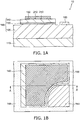
- FIGS. 1A and 1B are schematic views illustrating a structure of a semiconductor light-emitting element according to a first example useful for understanding the invention.
- FIG. 1B is a plan schematic view illustrating a structure of the semiconductor light-emitting element according to a first example useful for understanding the invention
- FIG. 1A is a schematic view of the A-A' line section.
- the semiconductor light-emitting element 10 has a first semiconductor layer 120, a second semiconductor layer 140, a light-emitting layer 130 provided between the first semiconductor layer 120 and the second semiconductor layer 140, and a first electrode 160 provided on the first semiconductor layer 120, and a second electrode 150 provided on the second semiconductor layer 140.
- the semiconductor light-emitting element 10 has a semiconductor layer 148 including the first semiconductor layer 120, the second semiconductor layer 140, and the light-emitting layer 130 sandwiched thereby.
- a nitride semiconductor such as Al x Ga 1-x-y In y N (1 ⁇ x ⁇ 0, 1 ⁇ y ⁇ 0, x+y ⁇ 1) can be used.
- this invention is not limited thereto.
- semiconductor having n-type conductivity can be used
- semiconductor having p-type conductivity can be used.
- the semiconductor layers (the first semiconductor layer 120, the light-emitting layer 130, and the second semiconductor layer 140) can be formed on a substrate 110.
- the method for forming the semiconductor layer 148 is not particularly limited, and a technique such as a metal organic chemical vapor deposition method and a molecular-beam epitaxial growth method can be used.
- the substrate 110 for example, sapphire, SiC, GaN, GaAs, Si, or the like can be used. In the case of using such a material of transmitting light emitted from the light-emitting layer 130 as sapphire, light can be taken out through the substrate 110. On the other hand, when the substrate 110 is formed by a material that does not transmit light emitted from the light-emitting layer 130, the light can also be taken out to the outside with reflected by the interface between the semiconductor layer 148 and the substrate 110. The substrate 110 may be removed on the way of the production of the semiconductor light-emitting element or after the production thereof. In this case, the light emitted from the light-emitting layer 130 can be taken out from the lower surface of the semiconductor layer 148 (the surface of the lower side in FIG. 1A ).
- the second electrode 150 for example, at least any one of silver and silver alloy can be used. However, this invention is not limited thereto, and in the second electrode 150, at least the side facing to the second semiconductor layer 140 may be made of at least any one of silver and silver alloy.
- a material of a conductive film to be the second electrode 150 may be a silver monolayer film or a silver alloy layer consisting of silver and metal except for silver.
- the reflection efficiencies of many metal monolayer films except for silver tend to decrease as the wavelength is shorter in the ultraviolet spectrum, but silver also has high reflection efficiency characteristic with respect to light of the ultraviolet spectrum of 370 nm to 400 nm. Therefore, by using silver or silver alloy as the second electrode 150, the light generated in the light-emitting layer 130, particularly light of ultraviolet spectrum is reflected high-efficiently, and the semiconductor light-emitting element 10 of high brightness can be realized.
- the conductive film to be the second electrode 150 when the conductive film to be the second electrode 150 is formed by silver alloy, it is preferable that the second semiconductor layer 140 side of the conductive film has a higher component ratio of silver than that of the other parts. It is preferable that the thickness of the conductive film to be the second electrode 150 is thicker than an inverse number of an absorption coefficient of silver for ensuring the reflection efficiency to light, and 100 nm or more is further preferable.
- the second electrode 150 has a void 210 having a width of emission wavelength or less of the light-emitting layer 130 in a plane of the second electrode facing to the second semiconductor layer.
- the void 210 the light pathway of the light emitted in the light-emitting layer 130 can be changed, the light trapping effect is suppressed by total internal reflection, and the semiconductor light-emitting element having high light taking-out efficiency can be provided.
- the void 210 is provided at least in the interface side of the electrode 150 to the second semiconductor layer 140, and the void 210 may also be provided in the interface of the second electrode 150 opposite to the second semiconductor layer 140 at the same time of being provided in the interface side of the electrode 150 to the second semiconductor layer 140. Moreover, the void 210 may also be provided in the layer of the second electrode 150 at the same time of being provided in the interface side of the electrode 150 to the second semiconductor layer 140, and furthermore, the void 210 may be provided so as to pass through the thickness direction of the second electrode 150. That is, it is sufficient that the void 210 is provided at least in the interface side of the electrode 150 to the second semiconductor layer 140, to which the light from the semiconductor layer 148 is incident.
- the void 210 of the second electrode 150 can be formed by self-assembly according to migration of silver by high-temperature heat treatment.
- the material of the first electrode 160 various monolayer films or multilayer films with conductivity that can be used as the ohmic electrode of the first semiconductor layer 120 can be used as the material of the first electrode 160.
- the method for forming the first electrode 160 is not particularly limited, but for example, it is possible that the multilayer structure is formed by an electron-beam deposition method and then sintering treatment is performed. In the case of performing the sintering treatment, it is preferable that a pad is provided separately in the first electrode 160 for improving bondability.
- a pad may be separately provided in the second electrode 150.
- the film thickness of the pad can be selected, for example, in 100 nm to 10000 nm.
- FIG. 2 is an enlarged schematic view illustrating a structure of a substantial part of the semiconductor light-emitting element according to the first example useful for understanding the invention.
- the light incident to the part except for the void 210 of the light emitted from the light-emitting layer 130 to the second electrode 150 is mirror-reflected according to geometric optics similarly to the light L.
- the width of the void 210 is smaller than the emission wavelength, the light incident to the void 210 shows behavior explained by wave optics such as scattering or diffraction. As a result, for example, lights XI, X2, and X3 scatter-reflected are generated.
- the region of scatter characteristic (diffuse reflection characteristic) can be formed in the interface between the second electrode 150 and the second semiconductor layer 140.
- lights having various angles such as light XI, X2, and X3 are generated, the incident angle of a part of the light that has a shallow incident angle with respect to the interface with refractive index difference (such as the interface between the semiconductor layer 148 and the substrate) and that is trapped inside the semiconductor light-emitting element 10 can be changed, and the light can be effectively taken out to the outside.
- the width of the void 210 becomes smaller than the emission wavelength, wave property of the light is enhanced and the scatter-reflected component of the light increases. As a result thereof, the light taking-out efficiency of the semiconductor light-emitting element 10 is improved.
- mirror reflection is reflection that the incident angle and the reflection angle of the light are equal as explained by geometric optics
- diffuse reflection is reflection that the light is scattered to all of the directions as explained by wave optics.
- the reflective index difference between the substrate 110 and the semiconductor layer 148 is large, and therefore, a large part of the emitted light are reflected on the interface and a large part of the emitted light is easily trapped inside the semiconductor layer 148.
- the semiconductor light-emitting element 10 according to this example useful for understanding the present invention by diffuse-reflecting the emitted light, the light can be effectively taken out to the outside, and therefore, the light taking-out efficiency is improved. As described above, it is effective to apply the semiconductor light-emitting element 10 according to this example useful for understanding the present invention to the semiconductor light-emitting element in which a sapphire substrate is used.
- FIGS. 3A and 3B are schematic views illustrating voids of the semiconductor light-emitting element according to the first example useful for understanding the invention.
- FIGS. 3A and 3B illustrate size (width) of voids when the voids have an elliptical shape and a shape except for elliptical shape, respectively.
- the width of the void 210 represents the long diameter S in the case that the sectional shape of the void 210 in the interface of the void 210 to the second semiconductor layer 140 is an elliptical shape ( FIG. 3A ), and the width of the void 210 represents the longest direct distance T in the void 210 in the other cases ( FIG. 3B ).
- the width of the void 210 becomes the above-described long diameter S or the direct distance T in the plane shape of the void 210 in the section of the plane of the second electrode 150 facing to the second semiconductor layer 140.
- the width of the void 210 is the emission wavelength or less.
- the emission spectrum of the semiconductor light-emitting element 10 has a half bandwidth of about several tens of nanometers. However, the emission wavelength represents the peak emission wavelength when the optical output becomes the maximum in the default operating current.
- the light When an action body such as the void 210 is sufficiently larger in comparison to the wavelength of the light, the light is treated as a light flux going straight and the behavior of the light is explained by geometric optics such as Snell's law.
- geometric optics such as Snell's law.
- the action body when the action body has approximately the same size as the wavelength of the light, the light increases its wave property, and phenomenon that cannot be explained by geometric optics is generated. Bending of the light is caused by the wave property such as diffraction or scattering.
- the wave property significantly appears in the region in which the size of the action body is the wavelength or less. In this region, the behavior of the light cannot be strictly calculated based on electromagnetics.
- a general semiconductor light-emitting element there are methods in which for improving the light taking-out efficiency, non-flat surfaces (convex-concave structure) are formed by processing, a substrate surface, inside of a semiconductor layer, and a surface of the semiconductor layer in contact with a reflection film.
- the surfaces formed by these methods have convex-concave structures with larger characters than the wavelength of the light and have mirror-reflection characteristics according to the geometric optics as viewed microscopically.
- the size of the void 210 is wavelength of the light or less, and has a characteristic of the wave property which cannot be explained by geometrical optics as described above.
- the density or the area ratio of the void 210 in the interface of the second electrode 150 to the second semiconductor layer 140 is higher, the light taking-out efficiency is higher.
- the density and the area ratio of the void 210 becomes too high, the contact area between the second electrode 150 and the second semiconductor layer 140 becomes small and the operation voltage occasionally becomes high.
- the area ratio of the void 210 with respect to the entire area of the second electrode 150 is 10 % or less, and 5 % or less is further preferable.
- the widths of the majority of these voids 210 are set to be wavelength or less of the emitted light. Thereby, more than half of the voids 210 generate diffraction or scattering based on the wave property of the light as described above, and the light taking-out efficiency can be improved.
- the average of the widths of these voids 210 is set to be wavelength of the emitted light or less.
- a large number of the voids generate diffraction or scattering based on the wave property of the light, and the light taking-out efficiency can be improved.
- FIG. 4 is a sectional schematic view illustrating a structure of the semiconductor light-emitting element according to the first reference example.
- a semiconductor light-emitting element 11 according to the first reference example has the same structure as the semiconductor light-emitting element 10 according to the first embodiment illustrated in FIGS. 1A and 1B .
- planar structure thereof can be the same as the semiconductor light-emitting element 10 according to this example useful for understanding the invention illustrated in FIGS. 1A and 1B , and therefore, the explanation thereof will be omitted.
- the semiconductor light-emitting element 11 has the semiconductor layer 148 in which on the substrate 110, a first AlN buffer layer 122 with a film thickness of 3 nm to 20 nm and a high carbon concentration (the carbon concentration is 3 x 10 18 cm -3 to 5 x 10 20 cm -3 ), a second AlN buffer layer 123 of high purity with a film thickness of 2 ⁇ m (the carbon concentration is 1 x 10 16 cm -3 to 3 x 10 18 cm -3 ), a non-doped GaN buffer layer 124 with a film thickness of 3 ⁇ m, a Si-doped n-type GaN contact layer 125 with a film thickness of 4 ⁇ m (the Si concentration is 1 x 10 16 cm -3 to 1 x 10 19 cm -3 ), a Si-doped n-type AlGaN clad layer 126 with a film thickness of 0.02 ⁇ m (the Si concentration is 1 x 10 16 cm -3 ), the light-emitting
- the semiconductor light-emitting element 11 has the second electrode (p-side electrode) 150 provided with a void having a width of wavelength of the light or less.
- the semiconductor light-emitting element with high light taking-out efficiency can be provided.
- the first AlN buffer layer 122, the second AlN buffer 123, the non-doped GaN buffer layer 124, the Si-doped n-type GaN contact layer 125, and the Si-doped n-type AlGaN clad layer 126 become the first semiconductor layer 120.
- the non-doped AlGaN spacer layer 142, the Mg-doped p-type AlGaN clad layer 143, the Mg-doped p-type GaN contact layer 144, and the high-concentration-Mg-doped p-type GaN contact layer 145 become the second semiconductor layer 140.
- the Mg-doped p-type GaN contact layer 144 and the high-concentration-Mg-doped p-type GaN contact layer 145 become a p-type GaN contact layer 146.
- the first AlN buffer layer 122 with a high carbon concentration functions to relax the mismatch of the lattice to the substrate 110, and particularly, reduces screw dislocation.
- the second AlN buffer layer 123 of high purity is a layer for planarizing the surface at the atomic level and reducing defects of the non-doped GaN buffer layer to be grown thereon, and it is preferable that the thickness thereof is thicker than 1 ⁇ m. Moreover, for preventing warpage due to strain, it is desirable that the thickness is 4 ⁇ m or less.
- the second AlN buffer layer of high purity is not limited to AlN, but Al x Ga 1-x N (0.8 ⁇ x ⁇ 1) is possible, the warpage of the wafer can be compensated.
- the non-doped GaN buffer layer 124 functions as defect reduction by 3-dimentional island growth on the second AlN buffer layer 123.
- the average film thickness of the non-doped GaN buffer layer 124 is 2 ⁇ m or more.
- the total film thickness of the non-doped GaN buffer layer 124 is 4 to 10 ⁇ m.
- the single crystal AlN buffer layer (the first AlN buffer layer 122, the second AlN buffer layer 123 of high purity, and the non-doped GaN buffer layer 124) like the semiconductor light-emitting element 11 according to this reference example, not only absorption in the buffer layer becomes difficult to be caused but also the defects in the semiconductor layer 148 is reduced, and therefore, factors causing light absorption in the semiconductor layer 148 can be reduced as much as possible, and the loss can be lowered. Therefore, by using the single crystal AlN buffer layer, even if density and area ratio of the voids 210 is lowered, high light taking-out efficiency can be obtained.
- the second electrode (p-side electrode) 150 provided with the void 210 having a width of wavelength of the light or less is used, and also, the single crystal AlN buffer layer is used, and therefore, absorption is difficult to be caused in the buffer layer, and the defects in the semiconductor layer decreases, and the factors causing light absorption in the semiconductor layer can be reduced as much as possible, and the semiconductor light-emitting element with high light taking-out efficiency can be provided.
- Mg concentration of the high-concentration-Mg-doped p-type GaN contact layer 145 is set to be at a level of 10 20 cm -3 , which is relatively high, ohmic property between the p-type GaN contact layer 146 and the second electrode 150 is improved.
- the distance between the high-concentration-Mg-doped p-type GaN contact layer 145 and the light-emitting layer 130 is small, and therefore, if the Mg concentration of the high-concentration-Mg-doped p-type GaN contact layer 145 is set to be high as described above, degradation of characteristics due to Mg diffusion is feared.
- the semiconductor light-emitting diode current density in the operation is low, and therefore, by suppressing the Mg concentration to be 10 19 cm -3 , the diffusion of Mg can be prevented without largely degrading the electric characteristics, and the light-emitting characteristics can be improved.
- the buffer layer is difficult to become an absorbing body to the emitted light, and the defects in the semiconductor layer 148 can be reduced, and the factors causing light absorption in the semiconductor layer 148 can be reduced as much as possible.
- the emitted light can repeat reflection at many times in the interface of the substrate 110 and the epitaxial layer and in the interface of the epitaxial layer and the p-side electrode 150, and therefore, the emitted light is trapped in the epitaxial layer and becomes easy to be affected by the void 210, and thereby, even if the density and the area ratio of the void 210 is low, high effect can be obtained.
- FIG. 5 is a flow chart illustrating a method for producing a semiconductor light-emitting element according to a second example useful for understanding the invention.
- a conductive film to be the second electrode (p-side electrode) 150 is formed (Step S110).
- This conductive film can include at least any one layer of silver and silver alloy.
- Step S120 At least any one of water and ionized substance is attached (Step S120).
- the void 210 having a width of emission wavelength or less of the emitting light of the semiconductor light-emitting element in at least a plane of the conductive film facing to the second semiconductor layer 140 by heat-treating the conductive film at a high temperature to make a gap in grain boundaries in the conductive film (Step S130).
- the method for producing the semiconductor light-emitting element of this example useful for understanding the present invention by making the conductive film to be the second electrode 150 migrate, a gap is made in grain boundaries in the conductive film, the void 210 having a width of wavelength or less of the emitted light can be easily formed in the conductive film like self-assembly, and the producing method by which the semiconductor light-emitting element with high light taking-out efficiency can be easily produced.
- a drying step for removing moisture attached to the surface of the semiconductor layer 148 and so forth can be provided before forming the above-described conductive film to be the second electrode 150. Moreover, as described later, by controlling temperature condition of the above-described high-temperature heat treatment and the temperature-lowering rate after the high-temperature heat treatment, generation of the void 210 can be controlled.
- the reference second example is an example of the above-described method for producing the semiconductor light-emitting element 11 according to the first reference example.
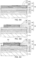
- FIGS. 6A to 6C are schematic sectional views following step sequence illustrating a part of the method for producing a semiconductor light-emitting element according to the second reference example.
- FIG. 6A is a view of a first step
- FIGS. 6B and 6C are views following the preceding views, respectively.
- the method for producing the semiconductor light-emitting element 11 according to the second reference example first by using a metal organic chemical vapor deposition, on the substrate 110 whose surface is composed of sapphire c surface, the first AlN buffer layer 122 with high carbon concentration, the second AlN buffer layer 123 of high purity, the non-doped GaN buffer layer 124, the Si-doped n-type GaN contact layer 125, the Si-doped n-type AlGaN clad layer 126, the light-emitting layer 130 having a multiquantum well structure in which Si-doped n-type AlGaN barrier layers and GaInN light-emitting layers are stacked alternately in three periods, the non-doped AlGaN spacer layer 142, the Mg-doped p-type AlGaN clad layer 143, the Mg-doped p-type GaN contact layer 144, and the high-concentration-Mg-d
- the p-type semiconductor layer (second semiconductor layer) 140 and the light-emitting layer 130 and the Si doped n-type AlGaN clad layer 126 were removed by dry etching by using a mask until the n-type contact layer 125 is exposed to the surface thereof.
- SiO 2 film 310 is stacked at a film thickness of 400 nm by using a thermal CVD (Chemical Vapor Deposition) apparatus.
- the p-side electrode 150 is formed thereon.
- the method for forming this p-side electrode 150 will be explained in detail. That is, hereinafter, only the region 300 shown in FIG. 6C in which the p-side electrode 150 is formed will be explained.
- FIGS. 7A to 7D are schematic sectional views following the step sequence of the substantial part illustrating the method for producing a semiconductor light-emitting element according to the second reference example.
- FIG. 7A is a view of a first step
- FIGS. 7B, 7C, and 7C are views following the preceding views, respectively.
- FIGS. 8A to 8D are schematic sectional views following the step sequence following FIGS. 7A to 7D .
- FIG. 7A is an enlarged schematic sectional view of the region 300 illustrated in FIG. 6C in which the SiO 2 film 310 is formed on the semiconductor layer.
- a lift-off resist 320 is formed in a predetermined pattern, and some of the SiO 2 film 310 on the p-type GaN contact layer 146 was removed by ammonium fluoride treatment, and moisture on the wafer (the substrate 110, the semiconductor layer 148, and the SiO 2 film 310 in this case) was blown off by an air blow or a spin dryer or the like.
- a conductive film 151 for forming the p-side electrode 150 was formed.
- This invention is not limited thereto, and for this conductive film 151, at least any one layer of silver and silver alloy can be used.
- the resist 320 was dissolved by an organic solvent, and thereby, only the conductive film 151 formed on the resist 320 was removed and sufficiently rinsed by ultrapure water, and then, the wafer was sufficiently dried on a hot plate at 120 °C. Thereby, the p-side electrode 150 was formed in the region in which the SiO 2 film 310 was removed.
- the wafer was kept in a clean room in which the temperature and the humidity were controlled to be 25 °C ⁇ 1 °C and 50 % ⁇ 1% respectively for 24 hours, and thereby, a little water (moisture) 330 and/or ionized substance 340 was attached to the surface of the formed p-side electrode 150.
- the SiO 2 film 310 on the n-type contact layer 125 exposed from the resist was removed by ammonium fluoride treatment.
- a vacuum deposition apparatus a thin film composed of Ti/Pt/Au was formed on the entire wafer at the film thickness of 500 nm, and by lift-off method, in the region in which the SiO 2 film 310 was removed, the n-side electrode 160 wafer was formed.
- the back surface of the substrate 110 was polished, and the wafer was cut by cleavage or diamond blade, and thereby the semiconductor light-emitting element could be formed.
- the void 210 can be formed by self-assembly according to migration of silver by high-temperature heat treatment.
- the temperature-lowering rate in the high-temperature heat treatment and after the heat treatment is set to be low, formation of the void 210 by the migration is performed with good reproducibility.
- the void 210 having a width of the wavelength or less can be formed with good reproducibility.
- the migration-promoting substance includes, for example, water, ionized substance (substance having relatively high ionization tendency and various compounds thereof), and various organic substances derived from the resist or the like.
- FIG. 9 is a schematic view showing behavior of crystal grain in heat treatment in the method for producing a semiconductor light-emitting element according to the second reference example.
- substance that is easy to migrate such as silver shows such behavior as the surface area becomes the smallest in the heat treatment, similarly to surface tension that is a property of liquid.
- the thermal stress is generated by the thermal expansion coefficient difference between the different kinds of materials, and the metal atoms move for trying to relax the stress.
- the metal atoms in the crystal grains 220 attracts each other to try to concentrate, the metal atoms in the vicinity of the gain boundary 230 diffuse and move to the center of the crystal grain 220, and the void 210 is generated in the grain boundaries 230.
- the surface roughness of the conductive film 151 is, for example, about 1.5 nm before the heat treatment, but after the heat treatment, the crystal grains 220 somewhat get moving, and therefore, the surface roughness increases to be, for example, about 2.5 nm.
- the heat treatment temperature is raised, the diffusion rate of the metal atoms becomes rapid according to Arrhenius' law, but the stress due to thermal stress becomes small.
- the width of the void 210 and the density of the void 210 in the plane of the p-side electrode 150 become a local maximal value in a certain heat treatment temperature.
- the width of the void 210, and the density and the area ratio in the plane of the p-side electrode 150 can be controlled by the state of the migration-promoting substance (namely, condition of the step for keeping the wafer for a certain time before the heat treatment, and so forth), the heat treatment (temperature, time, and temperature rising and lowering rates of the heat treatment), type, film thickness, and multilayer structure of the conductive film 151, and so forth.
- the void 210 can be formed in the interface of the semiconductor layer 148 side.
- the optical output is changed corresponding to density and area ratio of the void 210, and therefore, the above-described production condition can be changed considering the productivity and the optical output efficiency.
- the diffusion reflection region (void 210) can be formed by self-assembly, and the semiconductor light-emitting element can be realized at low cost.
- FIG. 10 is a sectional schematic view illustrating a structure of the semiconductor light-emitting element of the first comparative example.
- the void 210 is not provided in the second electrode 150.
- the structure except for this point is the same as the semiconductor light-emitting element 11 of the first reference example illustrated in FIG. 4 , and the explanation thereof will be omitted.
- the method for producing the semiconductor light-emitting element 91 of the first comparative example will be explained.
- the steps until forming the semiconductor layer 148 can be the same as the method for producing the semiconductor light-emitting element of the second reference example, and therefore, the producing method after the steps will be explained.
- FIGS. 11A to 11E are schematic views following the steps illustrating the method for producing the semiconductor light-emitting element of the first comparative example.
- FIG. 11A is a view of a first step
- FIGS. 11B and 11E are views following the preceding views, respectively.
- FIG. 11A is an enlarged view of the region 300 in which the SiO 2 film 310 is formed on the semiconductor layer.
- the lift-off resist 320 is formed in a predetermined pattern, and some of the SiO 2 film 310 on the p-type GaN contact layer 146 was removed by ammonium fluoride treatment, and moisture on the wafer was blown off by an air blow or a spin dryer or the like.
- the resist 320 was dissolved by an organic solvent, and thereby, only the conductive film 151 formed on the resist 320 was removed and rinsed by ultrapure water, and then, the wafer was dried. Thereby, the p-side electrode 150 was formed in the region in which the SiO 2 film 310 was removed.
- the drying step before forming the conductive film 151 for the p-side electrode 150 as illustrated in FIG. 7D and the step of attaching the migration-promoting substance as illustrated in FIG. 8C in the producing method of the second reference example of this invention are omitted.
- FIGS. 12A and 12B are scanning electron micrographs illustrating the structures of the surfaces of the second electrodes of the semiconductor light-emitting element according to the first reference example and the semiconductor light-emitting element of the first comparative example.
- FIG. 12A corresponds to the semiconductor light-emitting element 11 of the first reference example
- FIG. 12B corresponds to the semiconductor light-emitting element 91 of the first comparative example.
- the surface state was the same as the state before the heat treatment. That is, the void was not formed in the p-side electrode 150 of the semiconductor light-emitting element 91. And, in the evaluation of the surface roughness by the atom force microscope, the surface roughness was about 1.7 nm, which was the same as the surface roughness before the heat treatment.
- the upper side (opposite surface to the second semiconductor layer 120) of the granular image 291 is relatively flat and the surface roughness of the surface of the upper side of the part of the granular image 291 is about 2.6 nm, which is the same as the region except for the granular image 291, and that the granular image 291 is the void 210 formed in the interface of the p-side electrode 150 to the semiconductor layer 140. And, it was found that the upper side of the void 210 (the opposite side to the second semiconductor layer 140) is capped by the p-side electrode 150.
- the void 210 was formed in the grain boundaries 230 of the silver alloy of the p-side electrode 150.
- the conductive film 151 composed of Ag, Pt, and Ti is used as the p-side electrode 150.
- the metal layer having titanium as the main component is left in the surface, and by migration of Ag alloy, the void 210 is formed in the grain boundaries 230.
- the area ratio of the void 210 in the plane of the p-side electrode 150 was about 0.9 %.
- the flat region (gray level part of brightness in the figure) 292 having no void 210 shows an ohmic characteristic and a high efficient mirror-reflection characteristic, and the void 210 shows a diffuse reflection characteristic.
- the void 210 there is vacuum or a nitrogen gas of the heat treatment atmosphere, and the refraction indices of the both cases are thought to be about 1, and therefore, the refraction index difference between the void and the p-type GaN contact layer 146 is large and the structure easily generates total internal reflection.
- the void 210 because there is no light absorber in the void 210, absorption loss is small by repeating the reflection. Furthermore, in the void 210, it is thought that there is little moisture and little ionized substance, degradation of the p-side electrode 150 can be suppressed and therefore the reliability is improved.
- the semiconductor light-emitting element 11 According to the semiconductor light-emitting element 11 according to the first reference example, the semiconductor light-emitting element with high light taking-out efficiency and high reliability can be provided.
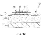
- FIG. 13 is a sectional schematic view illustrating a structure of the semiconductor light-emitting element according to a first embodiment of this invention.
- the semiconductor light-emitting element 30 As shown in FIG. 13 , the semiconductor light-emitting element 30 according to the first embodiment of this invention, the void 210 of the second electrode (p-side electrode) 150 is provided not only in the interface to the second semiconductor layer 140 but also continuously to the opposite surface to the second semiconductor layer 140 of the p-side electrode 150. That is, the void 210 is provided so as to pass through the layer of the p-side electrode 150 in the film-thickness direction.
- the semiconductor light-emitting element 30 has the same structure as the semiconductor light-emitting element 10 according to the first example useful for understanding the invention illustrated in FIGS. 1A and 1B except for the shape of the void 210, and also, the planar structure of the semiconductor light-emitting element 30 can be the same as the semiconductor light-emitting element 10, the explanation thereof will be omitted.
- the semiconductor light-emitting element 30 in which the void 210 is provided so as to pass through the p-side electrode 150 continuously in the thickness direction of the p-side electrode 150 the light path of the light generated in the light-emitting layer 130 can be changed by the void 210, and the light-trapping effect by the total internal reflection in the interface having the refraction index difference can be suppressed, and the semiconductor light-emitting element with high light taking-out efficiency can be provided.
- the buffer layer is difficult to become an absorber to the emitted light, and the defects in the semiconductor layer can be reduced, and the factor causing light absorption in the semiconductor layer can be reduced as much as possible.
- the emitted light can repeat reflection at many times in the interface between the epitaxial layer (semiconductor layer 148) and the p-side electrode 150, and therefore, the emitted light is trapped in the epitaxial layer (semiconductor layer 148) and easily affected by the effect in the 210, and thereby, even if the density or the area ratio of the void 210 is low, high light taking-out efficiency can be obtained.
- the method for producing the semiconductor light-emitting element of the first example is partial modification of the method for producing the semiconductor light-emitting element of the second reference example illustrated in FIGS. 6A to 8D . And, in this case, the heat treatment temperature of the p-side electrode 150 is changed to change the density of the void 210, and the relation between the void 210 and the optical output was investigated.
- FIG. 14A to 14G are schematic sectional views following step sequence of the substantial part illustrating the method for producing a semiconductor light-emitting element according to the first example of this invention.
- FIG. 14A is a view of a first step
- FIGS. 14B and 14G are views following the preceding views, respectively.
- the SiO 2 film 310 was provided on the semiconductor layer 148, and then for forming the p-side electrode 150, the patterned lift-off resist 320 was formed on the semiconductor layer 148, and some of the SiO 2 film on the p-type GaN contact layer 146 was removed by ammonium fluoride treatment.
- an Ag monolayer was formed at a film-thickness of 200 nm.
- the resist 320 was dissolved by an organic solvent, and thereby, only the conductive film 151 formed on the resist 320 was removed and sufficiently rinsed by ultrapure water, and then, the wafer was sufficiently dried on a hot plate at 120 °C. Thereby, the p-side electrode 150 was formed in the region in which the SiO 2 film 310 was removed.
- the wafer was kept in a clean room in which the temperature and the humidity were controlled to be 25 °C ⁇ 1 °C and 50 % ⁇ 1% respectively for 24 hours, and thereby, a little moisture 330 or ionized substance 340 was attached to the surface of the formed p-side electrode 150.
- the heat treatment was performed for 1 minute in an nitrogen atmosphere by three kinds of temperatures of 450 °C, 700 °C, and 800 °C, and the temperature was lowered at 5 °C/second to the normal temperature, and thereby, the void 210 was formed in the interface between the p-type GaN contact layer 146 and the p-side electrode 150.
- the first electrode (n-side electrode) 160 was formed in the same method as the second reference example, and thereby, the semiconductor light-emitting element of this example was formed.
- the p-side electrode was Ag, Pt, and Ti, and the heat treatment temperature by RTA was 800 °C.
- this example is different in the points that the p-side electrode 150 was an Ag monolayer and that the heat treatment temperature by RTA was changed to be the three kinds of 450 °C, 700 °C, and 800 °C.
- FIG. 15 is a scanning electron micrograph illustrating the structure of the surface of the second electrode of the semiconductor light-emitting element according to the first example of this invention.
- FIG. 15 is a photograph of a scanning electron microscopy imaging of the surface of the p-side electrode 150 of the semiconductor light-emitting element formed at the heat treatment temperature of 800 °C.
- granular images 291 having about a diameter of 0.1 ⁇ m on an average were observed.
- a scanning electron microscope or an atomic force microscope it was found that in the grain boundaries 230 of silver, a void 210 like a hole passing from the surface of the p-side electrode 150 to the p-type GaN contact layer 146 was formed. That is, it was found that by high-temperature heat treatment, Ag of the p-side electrode 150 migrated and the void 210 was formed in the grain boundaries 230.
- FIG. 16 is a graphic view illustrating the relation between the heat treatment temperature in the semiconductor light-emitting element according to the first example of this invention and the area ratio of the void of the semiconductor light-emitting element.
- the horizontal axis represents temperature of RTA heat treatment
- the vertical axis represents area ratio of the void 210 in the p-side electrode 150.
- the area ratios of the void 210 in the plane of p-side electrode 150 were 0.5 %, 1.2 %, 0.8 % in the heat treatment temperatures of 450 °C, 700 °C, and 800 °C, respectively.
- the area ratio of the void 210 indicates a local maximum value in the heat treatment temperature of 700 °C.
- the area ratio of the void 210 in the p-side electrode 150 indicates a local maximum value in a certain temperature as described above.
- the area ratio of the void 210 indicated the local maximum value in the heat treatment temperature of 700 °C.
- FIG. 17 is a graphic view illustrating the relation between the heat treatment temperature and the optical output of the semiconductor light-emitting element in the semiconductor light-emitting element according to the first example of this invention.
- the horizontal axis represents temperature of RTA heat treatment
- the vertical axis represents optical output of the semiconductor light-emitting element.
- the data that the heat treatment temperature in the figure is 350 °C represents the data of the comparative example in which the void is not formed in the p-side electrode 150.
- this figure illustrates the optical output of the semiconductor light-emitting element of this example as the relative ratio so that the optical output of the semiconductor light-emitting element of comparative example in which the void 210 is not formed in the p-side electrode 150 is 1.
- the optical output is large compared to the comparative example having no void, and that by forming the void 210, the optical output is improved by about 30 % at the maximum.
- the semiconductor light-emitting element of this example As described above, according to the semiconductor light-emitting element of this example, the semiconductor light-emitting element with high light taking-out efficiency can be provided.
- the semiconductor light-emitting elements of a second comparative example in which the void is not formed and a third comparative example in which the huge void with bad reproducibility is formed will be explained.
- FIGS. 18A to 18E are schematic sectional views following step sequence of the substantial part illustrating the method for producing a semiconductor light-emitting element of the second comparative example.
- FIG. 18A is a view of a first step
- FIGS. 18B to 18E are views following the preceding views, respectively.
- a lift-off resist 320 is formed in a predetermined pattern, and some of the SiO 2 film 310 on the p-type GaN contact layer 146 was removed by ammonium fluoride treatment, and moisture on the wafer was blown off by an air blow or a spin dryer or the like.
- a silver monolayer (the conductive film 151) was formed at a film-thickness of 200 nm, and then, the resist 320 was dissolved by an organic solvent, and thereby, only the conductive film 151 formed on the resist 320 was removed and sufficiently rinsed by ultrapure water, and then, the wafer was sufficiently dried on a hot plate at 120 °C. Thereby, the p-side electrode 150 was formed in the region in which the SiO 2 film 310 was removed.
- temperature of the wafer was raised to 800 °C at 5 °C/second in a nitrogen atmosphere, and the wafer was subjected to heat treatment for 1 minute in the nitrogen atmosphere at 800 °C, and the temperature was lowered to the normal temperature at 0.5 °C/second.
- the step for attaching the migration-promoting substance illustrated in FIG. 14F in the method for producing the semiconductor light-emitting element of the first example of this invention is omitted.
- FIGS. 19A to 19E are schematic sectional views following step sequence of the substantial part illustrating the method for producing a semiconductor light-emitting element of the third comparative example.
- FIG. 19A is a view of a first step
- FIGS. 19B to 19E are views following the preceding views, respectively.
- a lift-off resist 320 is formed in a predetermined pattern, and some of the SiO 2 film 310 on the p-type GaN contact layer 146 was removed by ammonium fluoride treatment, and moisture on the wafer was blown off by an air blow or a spin dryer or the like.
- a silver monolayer (the conductive film 151) was formed at a film-thickness of 200 nm.
- the resist 320 was dissolved by an organic solvent, and thereby, only the conductive film 151 formed on the resist 320 was removed and sufficiently rinsed by ultrapure water, and then, the wafer was sufficiently dried on a hot plate at 120 °C. Thereby, the p-side electrode 150 was formed in the region in which the SiO 2 film 310 was removed.
- temperature of the wafer was raised to 800 °C at 5 °C/second in a nitrogen atmosphere, and the wafer was subjected to heat treatment for 1 minute in the nitrogen atmosphere at 800 °C, and the temperature was lowered to the normal temperature at 0.5 °C/second.
- the drying step before film-forming the conductive film 151 for the p-side electrode 150 illustrated in FIG. 14C and the step for attaching the migration-promoting substance illustrated in FIG. 14F in the method for producing the semiconductor light-emitting element of the first example of this invention are omitted.
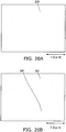
- FIGS. 20A and 20B are scanning electron micrographs illustrating structures of the surfaces of the second electrodes of the semiconductor light-emitting elements of the second and third comparative examples.
- FIG. 20A corresponds to the second comparative example and FIG. 20B corresponds to the third comparative example.
- the void was not formed at all.
- the image that can be seen in the figure is the grain boundary 230.
- the size (width) of the void enlarged to about 1 ⁇ m.
- the semiconductor light-emitting elements of the third comparative example were produced by the same process flow, but size and density of the void 210 did not have the reproducibility.
- the conductive film 151 to be the p-side electrode 150 was formed in the state of not sufficiently performing drying and the heat treatment was performed without sufficiently performing drying after the lift-off process, the migration of silver was excessively promoted and the void 210 became huge. Moreover, when the drying state was good by accident despite the same process flow, the size of the void 210 was suppressed, and consequently, the size of the void could not be controlled.
- the particular treatment such as the drying step before film-forming the conductive film 151 for the p-side electrode 150 or the step for attaching the migration-promoting substance
- the void 210 is not formed or the huge void 210 with low reproducibility becomes formed. Therefore, in forming the semiconductor light-emitting element according to this embodiment, the particular treatments such as the drying step before film-forming the conductive film 151 for the p-side electrode 150 and the step for attaching the migration-promoting substance are required as explained in the first example.
- the material used for the p-side electrode 150 is changed to Ag and Pt with respect to the semiconductor light-emitting element 30 according to the first embodiment explained previously.
- the other structure is the same as the semiconductor light-emitting element 30 according to the first embodiment, and the explanation thereof will be omitted.
- the method for producing the substantial part of the semiconductor light-emitting element 31 according to this example is as follows.
- the SiO 2 film was removed by ammonium fluoride treatment, and the moisture on the wafer was blown off, a little moisture remaining on the wafer surface was sufficiently dried and removed.
- a thin film (the conductive film 151) was formed in the order of Ag and Pt at a total film-thickness of 200 nm by a vacuum deposition apparatus on the entire wafer.
- the p-side electrode 150 was formed in the region in which the SiO 2 film 310 was removed.
- the wafer was kept in a clean room in which the temperature and the humidity were controlled to be 25 °C ⁇ 1 °C and 50 % ⁇ 1% respectively for 24 hours, and thereby, the migration-promoting substance (a little moisture 330 and/or ionized substance 340) was attached. Then, by using an RTA apparatus, the heat treatment was performed for 1 minute in a nitrogen atmosphere of 800 °C, and thereby, the void 210 was formed in the p-side electrode 150. That is, by the same condition as the semiconductor light-emitting element of the first example except for changing the material of the conductive film 151, the semiconductor light-emitting element according to this example was produced.
- FIG. 21 is a scanning electron micrograph illustrating structure of the surface of the second electrode of the semiconductor light-emitting element of the second example.
- the silver and platinum diffused to each other, and by the migration of the silver alloy, the void 210 was formed in the grain boundary.
- the area ratio of the void 210 in the plane of the p-side electrode 150 was 2.9%.
- the semiconductor light-emitting element 31 according to the second example by the void 210 having a width of the wavelength of the light or less provided in the p-side electrode 150, the semiconductor light-emitting element with high light taking-out efficiency can be provided.
- FIG. 22 is a sectional schematic view illustrating the structure of the semiconductor light-emitting element according to the second embodiment of this invention.
- the semiconductor light-emitting element 40 according to the second embodiment of this invention further includes a transparent electrode 410 provided between the second electrode 150 and the second semiconductor layer 140.
- the structures except for this transparent electrode 410 can be the same as the semiconductor light-emitting element 30 according to the first embodiment illustrated in FIG. 13 , and therefore, the explanation thereof will be explained.
- the second electrode 150 has the void passing through the layer of the second electrode 150.
- this invention is not limited thereto, but it is also possible that the void 210 is formed only in the interface of the second semiconductor layer 140 side of the second electrode 150 like the semiconductor light-emitting element 10 illustrated in FIGS. 1A and 1B .
- the transparent electrode 410 a substance having a larger band gap than the emission wavelength of the light-emitting layer 130 or a metal film having a sufficiently thinner film thickness than an inverse number in the emission wavelength can be used.
- the transparent electrode 410 for example, nickel, ITO (Indium-tin-oxide), zinc oxide, or the like can be used.
- the transparent electrode 410 is electrically in contact with the second semiconductor layer 140 and the second electrode 150.
- the transparent electrode 410 has a role of transmitting the light from the light-emitting layer 130 and reflecting the light by the second electrode 150, and therefore, it is preferable that the shape thereof in the planar view is substantially the same as the second electrode 150.
- the film thickness of the transparent electrode 410 is not particularly limited, and for example, can be selected from 1 nm to 500 nm.
- FIGS. 23A to 23G are schematic sectional views following step sequence of the substantial part illustrating the method for producing a semiconductor light-emitting element according to the second example of this invention.
- FIG. 23A is a view of a first step
- FIGS. 23B and 23G are views following the preceding views, respectively.
- the SiO 2 film 310 is provided on the semiconductor layer 148, and then for forming the p-side electrode 150, the patterned lift-off resist is formed on the semiconductor layer 148, and some of the SiO 2 film on the p-type GaN contact layer 146 is removed by ammonium fluoride treatment.
- ITO is formed at a film thickness of 100 nm by using a vacuum deposition apparatus, and after the lift-off process, the sintering treatment is performed for one minute in a nitrogen atmosphere of 550 °C, and thereby, the transparent electrode 410 is formed, and furthermore, a patterned lift-off resist 320 is formed on the semiconductor layer 148.
- the conductive film 151 to be the second electrode 150 such as an Ag monolayer is formed at a film-thickness of 200 nm.
- the resist 320 was dissolved by an organic solvent, and thereby, only the conductive film 151 formed on the resist 320 is removed and sufficiently rinsed by ultrapure water, and then, the wafer is sufficiently dried on a hot plate at 120 °C. Thereby, the p-side electrode 150 is formed in the region in which the SiO 2 film 310 is removed.
- the wafer is kept in a clean room in which the temperature and the humidity are controlled to be 25 °C ⁇ 1 °C and 50 % ⁇ 1% respectively for 24 hours, and thereby, a little moisture 330 and/or ionized substance 340 is attached to the surface of the formed p-side electrode 150.
- the heat treatment is performed for 1 minute in an nitrogen atmosphere of a temperature of 550 °C, and the temperature was lowered at 5 °C/second to the normal temperature, and thereby, the void 210 is formed in the interface between the p-type GaN contact layer 146 and the p-side electrode 150.
- the first electrode 160 is formed, and thereby, the semiconductor light-emitting element 40 according to this embodiment can be formed.
- the semiconductor light-emitting element 40 of this embodiment further having the transparent 410 between the second electrode 150 and the second semiconductor layer 140 produced as described above, the semiconductor light-emitting element with high light taking-out efficiency can be provided by the void 210 having an width of the wavelength of the light or less provided in the second electrode 150.
- the width of the void 210 and the density and the area ratio in the plane of the p-side electrode 150 can be changed by the heat treatment temperature and/or by type, film thickness, and multilayer structure of the metal material to be heat-treated at the same time as the conductive film 151.
- these conditions that are optimized for improving the optical output do not necessarily have the optimum combination with the electrical characteristic.
- the transparent electrode 410 is provided between the second electrode 150 and the second semiconductor layer 140 and the second electrode 150 functioning as a high efficient reflective film is provided through the transparent electrode 410 like the semiconductor light-emitting element 40 according to this embodiment, the optimized conditions for forming the void 210 with heavily weighting the optical-output improvement characteristic can be adopted, and thereby, the semiconductor light-emitting element with high light taking-out efficiency that can be more easily produced and that has higher performance can be provided.
- FIGS. 24A and 24B are schematic views illustrating a structure of the semiconductor light-emitting element according to the third embodiment of this invention.
- FIG. 24B is a plan schematic view illustrating the structure of the semiconductor light-emitting element according to the third embodiment of this invention
- the FIG. 24A is a sectional schematic view of the A-A' line.
- the semiconductor light-emitting element 50 has the above-described second electrode 150 having the void 210 and a third electrode 155, on the second semiconductor layer 140. And, the third electrode 155 is electrically in contact with the second electrode 150.
- the third electrode 155 can have a better ohmic property than the ohmic property of the second electrode 150.
- the position for providing the third electrode 155 is optional as long as being on the second semiconductor layer 140. However, as illustrated in FIGS. 24A and 24B , when the third electrode 155 is provided in contact with the first electrode 160 side of the second electrode 150, the conductive part having high ohmic property can be disposed in the region opposed to the first electrode 160, and therefore, stable electric characteristic can be obtained.
- the structure except for the third electrode 155 can be the same as the semiconductor light-emitting element 30 according to the first embodiment illustrated in FIG. 13 , and therefore, the explanation thereof will be omitted.
- the second electrode 150 has the void 210 passing through the layer of the second electrode 150.
- the semiconductor light-emitting element 50 according to this embodiment can be produced as follows.
- the second electrode 150 for example, Ag monolayer film having a film thickness of 200 nm
- a predetermined pattern having the void 210 is formed, and then, for example, an Ag/Pt film for forming the third electrode 155 is formed in a predetermined pattern at a film thickness of 200 nm, and by using an RTA apparatus, the heat treatment for 1 minute in an nitrogen atmosphere of 350, which is one of the conditions of not generating the void, is performed.
- the void is not generated in the third electrode 155, and the ohmic property thereof can be higher than that of the second electrode.
- the first electrode 160 is formed, and thereby, the semiconductor light-emitting element 50 illustrated in FIGS. 24 and 24B can be obtained.
- the width of the void 210 and the density and the area ratio in the plane of the p-side electrode 150 can be changed by the heat treatment temperature and/or by type, film thickness, and multilayer structure of the metal material to be heat-treated at the same time as the conductive film 151.
- these conditions that are optimized for improving the optical output do not necessarily have the optimum combination with the electrical characteristic.
- the current has a tendency of concentrating on the side of the second electrode 150 opposed to the first electrode 160.
- the effect appears more significantly as the current density is more enhanced.
- both of the light taking-out efficiency and the electrical characteristic can be highly satisfied. That is, various conditions for the second electrode 150 can be optimized by focusing attention on improving the light taking-out efficiency, and the various conditions for the third electrode 155 can be optimized by focusing attention on improving the electrical characteristic.
- the semiconductor light-emitting element with good electrical characteristic and high light taking-out efficiency can be provided.
- the area of the third electrode 155 in the planar view is more enlarged, the electrical characteristics are more improved, but the enlargement to an extent leads to saturation of the improvement.
- the effect thereof is higher as the area of the second electrode 150 is larger. Considering these effects, by adapting the second electrode 150 and the first electrode 160 to the design, the area of the third electrode 155 can be appropriately determined.
- the semiconductor light-emitting element 50 illustrated in FIGS. 24A and 24B has a structure in which the second electrode 150 is first formed and the third electrode 155 is provided so as to cover some of the second electrode 150.
- the third electrode 155 is first formed and the second electrode 150 is provided so as to cover some of the third electrode 155.
- the temperature of the high-temperature heat treatment of the third electrode 155 can be set to be higher than the temperature of the high-temperature heat treatment of the second electrode 150.
- the transparent electrode may be provided at least in a part between the second semiconductor layer 140 and at least any one of the second electrode 150 and the third electrode 155.
- the transparent electrode may be provided at least in a part between the second semiconductor layer 140 and at least any one of the second electrode 150 and the third electrode 155.
- FIG. 25 is a sectional schematic view illustrating a structure of the semiconductor light-emitting element according to a fourth embodiment of this invention.
- a pad 158 is provided in the surface of the second electrode 150 opposite to the second semiconductor layer 140.
- the structure except for the pad 158 is the same as the semiconductor light-emitting element 30 according to the first embodiment illustrated in FIG. 13 , and the explanation thereof will be omitted.
- the second electrode 150 has the void 210 passing through the layer of the second electrode 150.
- the pad 158 can be formed by, for example, forming Pt/Au at a film thickness of 800 nm so as to cover a part on the second electrode 150 or to cover the entire part containing the side surface of the second electrode 150 and then patterning the Pt/Au in a predetermined shape.
- the patterning for example, the lift-off method can be used.
- high-melting-point material such as not diffusing to the second electrode 150.
- the high-melting-point material include, for example, vanadium (V), chromium (Cr), iron (Fe), cobalt (Co), nickel (Ni), niobium (Ni), molybdenum (Mo), ruthenium (Ru), rhodium (Rh), tantalum (Ta), tungsten (W), rhenium (Re), osmium (Os), iridium (Ir), and platinum (Pt).
- Rhodium (Rh) or platinum (Pt) is particularly preferable, and has the reflective ratio with respect to the visible light that is high to some extent, and therefore, also functions as the reflective film.
- the bondability of the wire bonding can be improved, and the die shear strength in formation of gold bump with a ball bonder can be improved, and furthermore, this can be applied to the flip-chip mount. Furthermore, by the pad 158, the second electrode 150 is separated from the outside air, and degradation of the silver or the silver alloy can be suppressed, and the reliability thereof is improved. Furthermore, the improvement of the heat release property of the semiconductor light-emitting element 60 can be expected.
- This pad 158 can also be used as gold (Au) bump. Also, instead of Au, an AuSn bump can be formed.
- the semiconductor light-emitting element with high light taking-out efficiency that can be easily produced and that has high reliability and that has good heat release property can be provided.
- the above-described third electrode 155 in contact with the second electrode 150 may be provided, and the transparent electrode may be provided at least in a part between the second semiconductor layer 140 and at least any one of the second electrode 150 and the third electrode 155.
- FIG. 26 is a sectional schematic view illustrating another structure of the semiconductor light-emitting element according to a fourth embodiment of this invention.
- a pad 158 is provided in the surface of the second electrode 150 opposite to the second semiconductor layer 140. And, some of the void 210 of the second electrode 150 is buried with the conductive material to be the pad 158.
- the semiconductor light-emitting element 61 illustrated in FIG. 26 has, for example, a structure in which the second electrode 150 has the void 210 passing through the layer of the second electrode 150 on the way of the production and some of the void 210 is buried by the subsequent formation of the pad 158.
- the structure except for the void 210 is the same as the semiconductor light-emitting element 60 illustrated in FIG. 25 , and therefore, the explanation thereof will be omitted.
- a part 210A out of the void 210 is buried by the pad 158 but the space remains in the interface of the second semiconductor layer 140.
- the entirety of the void is buried with the material to be the pad 158.
- the light taking-out efficiency is improved by the same effect as explained previously.
- the light taking-out efficiency is improved by the following effect.
- the difference of the complex refractive index between the both can be generated, and thereby, the diffuse reflection is generated, and the light taking-out efficiency can be improved.
- the wavelength in a medium is a value of the wavelength in a free space of the emitted light divided by the refractive index of the medium and becomes shorter than the wavelength in a free space.
- the wavelength in the medium becomes about 150 nm.
- the width of the void 210 is set to be the same length or less as the wavelength in the medium.
- the refractive index in the void 210 is about 1 without changing before and after the formation of the pad 158, and therefore, it is sufficient that the width of the void 210 is almost the same length or less as the wavelength in a free space.
- the diffuse reflection can be generated, and the semiconductor light-emitting element with high light taking-out efficiency can be provided.
- the above-described third electrode 155 in contact with the second electrode 150 may be provided, and the transparent electrode may be provided at least in a part between the second semiconductor layer 140 and at least any one of the second electrode 150 and the third electrode 155.
- the semiconductor light-emitting element according to this embodiment is a semiconductor light-emitting element in which the above-described semiconductor light-emitting element of each of the embodiments and each of the examples and a fluorescent material are combined.
- FIG. 27 is a sectional schematic view illustrating a structure of the semiconductor light-emitting element according to the fifth embodiment of this invention.
- the semiconductor light-emitting element 70 includes, for example, the semiconductor light-emitting element 30 of the first embodiment and a fluorescent material layer 530 that can be excited by the light emitted in the semiconductor light-emitting element 30 to emit a fluorescent light.
- a reflective film 520 is provided in the inner surface of the container 510 made of ceramics or the like.
- the reflective film 520 is provided so as to be divided into the reflective film 521 on the bottom surface of the container 510 and the reflective film 522 on the side surface of the container 510.
- aluminum or the like can be used for the reflective film 520.
- the semiconductor light-emitting element 30 is disposed through a submount 524.
- a gold bump 528 is formed by a ball bonder, and the semiconductor light-emitting element 30 is fixed to the submount 524. It is also possible that without using the gold bump 528, the semiconductor light-emitting element 30 is fixed to the submount 524.
- adhesion by an adhesive agent or solder or the like can be used for the fixation of the semiconductor light-emitting element 30, the submount 524, and the reflection film 520.
- patterned electrodes are formed so as to be insulated with respect to the second electrode (p-side electrode) 150 and the first electrode (n-side electrode) 160 of the semiconductor light-emitting element 30, and the respective patterned electrodes are connected to the electrodes (not shown in figure) provided in the container 510 side, with the bonding wires 526.
- the connections are performed in parts between the reflective film 522 of the side surface and the reflective film 521 of the bottom surface.
- the fluorescent material layer 530 is provided so as to cover the semiconductor light-emitting element 30 and the bonding wires 526.
- a first fluorescent material layer 531 containing a red fluorescent material and a second fluorescent material layer 532 provided on the first fluorescent material layer 531 and containing a blue, green or yellow fluorescent material are provided.
- a lid 512 made of silicon resin is provided on these fluorescent material layers 530.
- the first fluorescent material layer 531 includes a resin and a red fluorescent material dispersed in the resin.
- a red fluorescent material for example, Y 2 O 3 , YVO 4 , Y 2 (P,V)O 4 or the like can be used as the base material, and trivalent Eu (Eu 3+ ) is contained therein as the activation substance. That is, Y 2 O 3 :Eu 3+ , YVO 4 :Eu 3+ , or the like can be used as the red fluorescent material.
- the concentration of Eu 3+ can be 1 % to 10 % by molar concentration.
- the base material of the red fluorescent material as well as Y 2 O 3 or YVO 4 , LaOS or Y 2 (P,V)O 4 or the like can be used.
- Eu 3+ , Mn 4+ , or the like can be utilized.
- the resin for example, silicon resin or the like can be used.
- the second fluorescent material layer 532 includes a resin and a fluorescent material that is at least any one of blue, green, and yellow and that is dispersed in the resin.
- the fluorescent material in which the blue fluorescent material and the green fluorescent material are combined may be used, or the fluorescent material in which the blue fluorescent material and the yellow fluorescent material are combined may be used, or the fluorescent material in which the blue fluorescent material, the green fluorescent material, and the yellow fluorescent material are combined may be used.
- blue fluorescent material for example, (Sr,Ca) 10 (PO 4 ) 6 Cl 2 :Eu 2+ or BaMg 2 Al 16 O 27 :Eu 2+ or the like can be used.
- the green fluorescent material for example, Y 2 SiO 5 :Ce 3+ ,Tb 3+ in which the trivalent Tb is the emission center can be used. In this case, because the energy is transfer from Ce ion to Tb ion, the excitation efficiency is improved.
- the green fluorescent material for example, Sr 4 Al 14 O 25 :Eu 2+ or the like can be used.
- yellow fluorescent material for example, Y 3 Al 5 :Ce 3+ or the like can be used.
- resin for example, silicon resin or the like can be used.
- the trivalent Tb indicates sharp emission in the vicinity of 550 nm, in which the visibility becomes the maximum, and therefore, when the trivalent Tb is combined with the sharp red emission of Eu, the emission efficiency is significantly improved.
- the ultraviolet light of 380 nm generated from the semiconductor light-emitting element 30 is emitted to the substrate side of the semiconductor light-emitting element 30, and the reflection in the reflective films 521, 522 is also utilized, and thereby, the above-described fluorescent materials contained in the respective fluorescent material layers can be efficiently excited.
- the light is converted into a light having the wavelength distribution of the vicinity of 620 nm, and thereby the red visible light can be efficiently obtained.
- the blue, green, or yellow fluorescent material contained in the second fluorescent material layer 532 is efficiently excited, and thereby, the blue, green, or yellow visible light can be efficiently obtained.
- the steps for producing the semiconductor light-emitting element 30 are the same as explained previously.
- the metal film to be the reflective film is formed on the inner surface of the container 510 by, for example, a sputtering method, and the metal film is patterned to form the reflective films 521, 522 in the bottom surface and the side surface of the container 510, respectively.
- the gold bumps 528 are formed by a ball bonder.
- the semiconductor light-emitting element 30 is fixed, and the submount 524 is disposed and fixed onto the reflective film 521 of the bottom surface of the container 510.
- adhesion by an adhesive agent or solder or the like can be used.
- the semiconductor light-emitting element 30 is directly fixed onto the submount 524.
- the first electrode 160 and the second electrode 150 (not shown) on the submount 524 are connected to the electrodes (not shown) provided in the container 510 side, respectively, with bonding wires 526. Furthermore, the first fluorescent material layer 531 is formed so as to cover the semiconductor light-emitting element 30 or the bonding wires 526, and the second fluorescent material layer 532 is formed on the first fluorescent material layer 531.
- a method of dropping each of the fluorescent materials dispersed in the resin material mixtures and then performing thermal polymerization by heat treatment to harden the resin can be used.
- the lid 512 is provided on the fluorescent material layer, and thereby, the semiconductor light-emitting element 70 according to this embodiment, namely, white LED is produced.
- the semiconductor light-emitting element 70 of this embodiment the semiconductor light-emitting element with high light taking-out efficiency that can generate various colors with high efficiency can be provided.
- the example in which the first semiconductor layer 120 is an n-type semiconductor layer and the second semiconductor layer 140 is a p-type semiconductor layer has been presented.
- this invention is not limited thereto, and the conductivity types can be inverted.
- nitride semiconductor includes all of the semiconductors having the compositions in which the composition ratios x, y, and z are changed in the respective ranges in the chemical formula of B x In y Al z Ga 1-x-y-z N (0 ⁇ x ⁇ 1, 0 ⁇ y ⁇ 1, 0 ⁇ z ⁇ 1, x+y+z ⁇ 1).
- the semiconductor further containing a group V element except for N (nitrogen) or the semiconductor further containing any one of various dopants to be added for controlling the conductivity type and so forth is also included in the "nitride semiconductor".
Landscapes
- Led Devices (AREA)
- Led Device Packages (AREA)
Applications Claiming Priority (1)
| Application Number | Priority Date | Filing Date | Title |
|---|---|---|---|
| JP2008062611A JP5047013B2 (ja) | 2008-03-12 | 2008-03-12 | 半導体発光素子及びその製造方法 |
Publications (3)
| Publication Number | Publication Date |
|---|---|
| EP2101363A2 EP2101363A2 (en) | 2009-09-16 |
| EP2101363A3 EP2101363A3 (en) | 2014-08-20 |
| EP2101363B1 true EP2101363B1 (en) | 2018-06-06 |
Family
ID=40933169
Family Applications (1)
| Application Number | Title | Priority Date | Filing Date |
|---|---|---|---|
| EP09250663.3A Active EP2101363B1 (en) | 2008-03-12 | 2009-03-10 | Semiconductor light-emitting element and method for producing the same |
Country Status (3)
| Country | Link |
|---|---|
| US (4) | US8017970B2 (https=) |
| EP (1) | EP2101363B1 (https=) |
| JP (1) | JP5047013B2 (https=) |
Families Citing this family (15)
| Publication number | Priority date | Publication date | Assignee | Title |
|---|---|---|---|---|
| US7577453B2 (en) | 2006-06-01 | 2009-08-18 | Trapeze Networks, Inc. | Wireless load balancing across bands |
| US7950643B2 (en) | 2007-09-04 | 2011-05-31 | Kabushiki Kaisha Toshiba | Sheet finisher, image forming apparatus using the same, and sheet finishing method |
| JP2010219377A (ja) * | 2009-03-18 | 2010-09-30 | Toshiba Corp | 半導体発光装置及びその製造方法 |
| US20100327300A1 (en) * | 2009-06-25 | 2010-12-30 | Koninklijke Philips Electronics N.V. | Contact for a semiconductor light emitting device |
| KR20120092325A (ko) * | 2011-02-11 | 2012-08-21 | 서울옵토디바이스주식회사 | 광 결정 구조를 갖는 발광 다이오드 및 그것을 제조하는 방법 |
| JP4989773B1 (ja) | 2011-05-16 | 2012-08-01 | 株式会社東芝 | 半導体発光素子 |
| TW201301588A (zh) * | 2011-06-30 | 2013-01-01 | 兆鑫光電科技股份有限公司 | 大發光面積的發光二極體晶粒及其封裝結構 |
| JP2013140948A (ja) * | 2011-12-09 | 2013-07-18 | Toshiba Corp | 半導体発光素子及びその製造方法 |
| KR101976450B1 (ko) * | 2012-10-19 | 2019-05-09 | 엘지이노텍 주식회사 | 발광 소자 및 발광 소자 패키지 |
| TWI604632B (zh) | 2013-04-25 | 2017-11-01 | 晶元光電股份有限公司 | 發光二極體裝置 |
| FR3005784B1 (fr) * | 2013-05-14 | 2016-10-07 | Aledia | Dispositif optoelectronique et son procede de fabrication |
| JP2014099663A (ja) * | 2014-03-04 | 2014-05-29 | Toshiba Corp | 半導体発光素子 |
| JP2016046411A (ja) * | 2014-08-25 | 2016-04-04 | シャープ株式会社 | 半導体発光素子 |
| JP6793815B2 (ja) * | 2017-03-27 | 2020-12-02 | Dowaエレクトロニクス株式会社 | Iii族窒化物半導体発光素子およびその製造方法 |
| US11978839B2 (en) * | 2019-02-03 | 2024-05-07 | Quanzhou Sanan Semiconductor Technology Co., Ltd. | Light-emitting device |
Citations (2)
| Publication number | Priority date | Publication date | Assignee | Title |
|---|---|---|---|---|
| US6291839B1 (en) * | 1998-09-11 | 2001-09-18 | Lulileds Lighting, U.S. Llc | Light emitting device having a finely-patterned reflective contact |
| US20070023777A1 (en) * | 2004-10-19 | 2007-02-01 | Shinya Sonobe | Semiconductor element |
Family Cites Families (21)
| Publication number | Priority date | Publication date | Assignee | Title |
|---|---|---|---|---|
| JP3559453B2 (ja) * | 1998-06-29 | 2004-09-02 | 株式会社東芝 | 発光素子 |
| DK1371120T3 (da) * | 2001-03-09 | 2013-07-22 | Alight Photonics Aps | Bølgetypekontrol ved anvendelse af transversal båndgabsstruktur i vcsels |
| JP3866540B2 (ja) * | 2001-07-06 | 2007-01-10 | 株式会社東芝 | 窒化物半導体素子およびその製造方法 |
| WO2003025263A1 (en) * | 2001-09-13 | 2003-03-27 | Japan Science And Technology Agency | Nitride semiconductor substrate, its manufacturing method, and semiconductor optical device using the same |
| JP2004014943A (ja) * | 2002-06-10 | 2004-01-15 | Sony Corp | マルチビーム型半導体レーザ、半導体発光素子および半導体装置 |
| KR20050051920A (ko) * | 2003-11-28 | 2005-06-02 | 삼성전자주식회사 | 플립칩형 질화물계 발광소자 및 그 제조방법 |
| JP2006041498A (ja) * | 2004-06-24 | 2006-02-09 | Showa Denko Kk | 反射性正極およびそれを用いた窒化ガリウム系化合物半導体発光素子 |
| JP4869582B2 (ja) * | 2004-11-29 | 2012-02-08 | シャープ株式会社 | 半導体レーザ素子、光ディスク装置および光伝送システム |
| US20060170022A1 (en) * | 2005-01-31 | 2006-08-03 | Klaus Ufert | Silicon molecular hybrid storage cell |
| JP5008263B2 (ja) * | 2005-03-02 | 2012-08-22 | 日亜化学工業株式会社 | 半導体発光素子 |
| JP4653671B2 (ja) * | 2005-03-14 | 2011-03-16 | 株式会社東芝 | 発光装置 |
| KR100878433B1 (ko) * | 2005-05-18 | 2009-01-13 | 삼성전기주식회사 | 발광소자의 오믹컨택층 제조방법 및 이를 이용한발광소자의 제조방법 |
| JP2007005591A (ja) | 2005-06-24 | 2007-01-11 | Toshiba Corp | 半導体発光素子 |
| US7638810B2 (en) * | 2005-09-09 | 2009-12-29 | Avago Technologies Ecbu Ip (Singapore) Pte. Ltd. | GaN laser with refractory metal ELOG masks for intracavity contact |
| US7873090B2 (en) * | 2005-09-13 | 2011-01-18 | Panasonic Corporation | Surface emitting laser, photodetector and optical communication system using the same |
| JP4688674B2 (ja) * | 2005-10-20 | 2011-05-25 | 京セラ株式会社 | 発光素子収納用パッケージおよび発光装置 |
| JP5037835B2 (ja) * | 2006-02-28 | 2012-10-03 | キヤノン株式会社 | 垂直共振器型面発光レーザ |
| JP2008062611A (ja) | 2006-09-11 | 2008-03-21 | Sekisui Film Kk | 積層フィルム及び積層体 |
| TW200945627A (en) * | 2007-12-07 | 2009-11-01 | Alps Electric Co Ltd | Semiconductor light-emitting device |
| KR101007117B1 (ko) * | 2008-10-16 | 2011-01-11 | 엘지이노텍 주식회사 | 반도체 발광소자 및 그 제조방법 |
| JP4772168B2 (ja) * | 2009-09-30 | 2011-09-14 | 京セラ株式会社 | 発光素子、および発光素子の製造方法 |
-
2008
- 2008-03-12 JP JP2008062611A patent/JP5047013B2/ja active Active
-
2009
- 2009-03-10 EP EP09250663.3A patent/EP2101363B1/en active Active
- 2009-03-10 US US12/401,473 patent/US8017970B2/en active Active
-
2011
- 2011-01-19 US US12/929,365 patent/US8377724B2/en active Active
-
2013
- 2013-01-18 US US13/744,437 patent/US8729594B2/en active Active
-
2014
- 2014-04-04 US US14/244,915 patent/US9373752B2/en active Active
Patent Citations (2)
| Publication number | Priority date | Publication date | Assignee | Title |
|---|---|---|---|---|
| US6291839B1 (en) * | 1998-09-11 | 2001-09-18 | Lulileds Lighting, U.S. Llc | Light emitting device having a finely-patterned reflective contact |
| US20070023777A1 (en) * | 2004-10-19 | 2007-02-01 | Shinya Sonobe | Semiconductor element |
Also Published As
| Publication number | Publication date |
|---|---|
| US20130134458A1 (en) | 2013-05-30 |
| US9373752B2 (en) | 2016-06-21 |
| US20090230422A1 (en) | 2009-09-17 |
| JP2009218483A (ja) | 2009-09-24 |
| US20110117684A1 (en) | 2011-05-19 |
| US8377724B2 (en) | 2013-02-19 |
| EP2101363A3 (en) | 2014-08-20 |
| JP5047013B2 (ja) | 2012-10-10 |
| US8017970B2 (en) | 2011-09-13 |
| US20140217360A1 (en) | 2014-08-07 |
| EP2101363A2 (en) | 2009-09-16 |
| US8729594B2 (en) | 2014-05-20 |
Similar Documents
| Publication | Publication Date | Title |
|---|---|---|
| EP2101363B1 (en) | Semiconductor light-emitting element and method for producing the same | |
| JP5191837B2 (ja) | 半導体発光素子及び半導体発光装置 | |
| US9070837B2 (en) | Semiconductor light-emitting device and method for manufacturing same | |
| JP5325506B2 (ja) | 半導体発光素子及びその製造方法 | |
| JP5139005B2 (ja) | 半導体発光素子及び半導体発光装置 | |
| JP5334601B2 (ja) | 半導体発光ダイオード素子及び半導体発光装置 | |
| JP5862354B2 (ja) | 窒化物系発光ダイオード素子とその製造方法 | |
| JP4765632B2 (ja) | 半導体発光素子 | |
| US7902565B2 (en) | Semiconductor light emitting device and method for manufacturing same | |
| JP5608762B2 (ja) | 半導体発光素子 | |
| JP2013211598A (ja) | 半導体発光ダイオード素子及び半導体発光装置 | |
| JP5319820B2 (ja) | 半導体発光ダイオード素子及び半導体発光装置 | |
| JP5851001B2 (ja) | 半導体発光素子 | |
| KR102000271B1 (ko) | 질화갈륨 계열 발광 다이오드의 제조방법 및 이로부터 제조된 질화갈륨 계열 발광 다이오드 | |
| JP5368609B2 (ja) | 半導体発光素子の製造方法 | |
| JP5602916B2 (ja) | 半導体発光素子 | |
| JP5372220B2 (ja) | 半導体発光素子及び半導体発光装置 | |
| JP5886899B2 (ja) | 半導体発光素子及び半導体発光装置 | |
| JP5563031B2 (ja) | 半導体発光素子及び半導体発光装置 |
Legal Events
| Date | Code | Title | Description |
|---|---|---|---|
| PUAI | Public reference made under article 153(3) epc to a published international application that has entered the european phase |
Free format text: ORIGINAL CODE: 0009012 |
|
| 17P | Request for examination filed |
Effective date: 20090316 |
|
| AK | Designated contracting states |
Kind code of ref document: A2 Designated state(s): AT BE BG CH CY CZ DE DK EE ES FI FR GB GR HR HU IE IS IT LI LT LU LV MC MK MT NL NO PL PT RO SE SI SK TR |
|
| AX | Request for extension of the european patent |
Extension state: AL BA RS |
|
| PUAL | Search report despatched |
Free format text: ORIGINAL CODE: 0009013 |
|
| AK | Designated contracting states |
Kind code of ref document: A3 Designated state(s): AT BE BG CH CY CZ DE DK EE ES FI FR GB GR HR HU IE IS IT LI LT LU LV MC MK MT NL NO PL PT RO SE SI SK TR |
|
| AX | Request for extension of the european patent |
Extension state: AL BA RS |
|
| RIC1 | Information provided on ipc code assigned before grant |
Ipc: H01L 33/32 20100101ALI20140716BHEP Ipc: H01L 33/40 20100101ALI20140716BHEP Ipc: H01L 33/00 20100101AFI20140716BHEP Ipc: H01L 33/38 20100101ALI20140716BHEP |
|
| AKX | Designation fees paid |
Designated state(s): DE FR GB |
|
| AXX | Extension fees paid |
Extension state: AL Extension state: BA Extension state: RS |
|
| 17Q | First examination report despatched |
Effective date: 20160921 |
|
| STAA | Information on the status of an ep patent application or granted ep patent |
Free format text: STATUS: EXAMINATION IS IN PROGRESS |
|
| RIC1 | Information provided on ipc code assigned before grant |
Ipc: H01L 33/32 20100101ALI20171222BHEP Ipc: H01L 33/38 20100101ALI20171222BHEP Ipc: H01L 33/42 20100101ALI20171222BHEP Ipc: H01L 33/40 20100101ALI20171222BHEP Ipc: H01L 33/00 20100101AFI20171222BHEP |
|
| GRAP | Despatch of communication of intention to grant a patent |
Free format text: ORIGINAL CODE: EPIDOSNIGR1 |
|
| STAA | Information on the status of an ep patent application or granted ep patent |
Free format text: STATUS: GRANT OF PATENT IS INTENDED |
|
| INTG | Intention to grant announced |
Effective date: 20180226 |
|
| GRAS | Grant fee paid |
Free format text: ORIGINAL CODE: EPIDOSNIGR3 |
|
| GRAA | (expected) grant |
Free format text: ORIGINAL CODE: 0009210 |
|
| STAA | Information on the status of an ep patent application or granted ep patent |
Free format text: STATUS: THE PATENT HAS BEEN GRANTED |
|
| RIN1 | Information on inventor provided before grant (corrected) |
Inventor name: KEI, KANEKO Inventor name: HIROSHI, KATSUNO Inventor name: YASUO, OHBA |
|
| AK | Designated contracting states |
Kind code of ref document: B1 Designated state(s): DE FR GB |
|
| REG | Reference to a national code |
Ref country code: GB Ref legal event code: FG4D |
|
| REG | Reference to a national code |
Ref country code: DE Ref legal event code: R096 Ref document number: 602009052647 Country of ref document: DE |
|
| REG | Reference to a national code |
Ref country code: GB Ref legal event code: 732E Free format text: REGISTERED BETWEEN 20180628 AND 20180706 |
|
| RAP2 | Party data changed (patent owner data changed or rights of a patent transferred) |
Owner name: TOSHIBA ELECTRONIC DEVICES & STORAGE CORPORATION |
|
| REG | Reference to a national code |
Ref country code: DE Ref legal event code: R082 Ref document number: 602009052647 Country of ref document: DE Representative=s name: HOFFMANN - EITLE PATENT- UND RECHTSANWAELTE PA, DE Ref country code: DE Ref legal event code: R081 Ref document number: 602009052647 Country of ref document: DE Owner name: SAMSUNG ELECTRONICS CO., LTD., SUWON-SI, KR Free format text: FORMER OWNER: KABUSHIKI KAISHA TOSHIBA, TOKIO/TOKYO, JP Ref country code: DE Ref legal event code: R082 Ref document number: 602009052647 Country of ref document: DE Representative=s name: KUHNEN & WACKER PATENT- UND RECHTSANWALTSBUERO, DE |
|
| REG | Reference to a national code |
Ref country code: DE Ref legal event code: R081 Ref document number: 602009052647 Country of ref document: DE Owner name: SAMSUNG ELECTRONICS CO., LTD., SUWON-SI, KR Free format text: FORMER OWNER: TOSHIBA ELECTRONIC DEVICES & STORAGE CORPORATION, TOKYO, JP Ref country code: DE Ref legal event code: R082 Ref document number: 602009052647 Country of ref document: DE Representative=s name: KUHNEN & WACKER PATENT- UND RECHTSANWALTSBUERO, DE Ref country code: DE Ref legal event code: R081 Ref document number: 602009052647 Country of ref document: DE Owner name: SAMSUNG ELECTRONICS CO., LTD., SUWON-SI, KR Free format text: FORMER OWNER: TOSHIBA ELECTRONIC DEVICES & STORAGE CORP., TOKYO, JP |
|
| RAP2 | Party data changed (patent owner data changed or rights of a patent transferred) |
Owner name: SAMSUNG ELECTRONICS CO., LTD. |
|
| RIC2 | Information provided on ipc code assigned after grant |
Ipc: H01L 33/00 20100101AFI20171222BHEP Ipc: H01L 33/40 20100101ALI20171222BHEP Ipc: H01L 33/38 20100101ALI20171222BHEP Ipc: H01L 33/32 20100101ALI20171222BHEP Ipc: H01L 33/42 20100101ALI20171222BHEP |
|
| REG | Reference to a national code |
Ref country code: GB Ref legal event code: 732E Free format text: REGISTERED BETWEEN 20190124 AND 20190130 |
|
| REG | Reference to a national code |
Ref country code: DE Ref legal event code: R097 Ref document number: 602009052647 Country of ref document: DE |
|
| PLBE | No opposition filed within time limit |
Free format text: ORIGINAL CODE: 0009261 |
|
| STAA | Information on the status of an ep patent application or granted ep patent |
Free format text: STATUS: NO OPPOSITION FILED WITHIN TIME LIMIT |
|
| 26N | No opposition filed |
Effective date: 20190307 |
|
| P01 | Opt-out of the competence of the unified patent court (upc) registered |
Effective date: 20230520 |
|
| REG | Reference to a national code |
Ref country code: DE Ref legal event code: R079 Ref document number: 602009052647 Country of ref document: DE Free format text: PREVIOUS MAIN CLASS: H01L0033000000 Ipc: H10H0020000000 |
|
| PGFP | Annual fee paid to national office [announced via postgrant information from national office to epo] |
Ref country code: GB Payment date: 20260128 Year of fee payment: 18 |
|
| PGFP | Annual fee paid to national office [announced via postgrant information from national office to epo] |
Ref country code: DE Payment date: 20260128 Year of fee payment: 18 |
|
| PGFP | Annual fee paid to national office [announced via postgrant information from national office to epo] |
Ref country code: FR Payment date: 20260121 Year of fee payment: 18 |