EP2091237B1 - Dispositif de capture d'images - Google Patents
Dispositif de capture d'images Download PDFInfo
- Publication number
- EP2091237B1 EP2091237B1 EP09250341.6A EP09250341A EP2091237B1 EP 2091237 B1 EP2091237 B1 EP 2091237B1 EP 09250341 A EP09250341 A EP 09250341A EP 2091237 B1 EP2091237 B1 EP 2091237B1
- Authority
- EP
- European Patent Office
- Prior art keywords
- image
- mtf correction
- correction
- illuminance
- pickup device
- Prior art date
- Legal status (The legal status is an assumption and is not a legal conclusion. Google has not performed a legal analysis and makes no representation as to the accuracy of the status listed.)
- Ceased
Links
Images

Classifications
-
- H—ELECTRICITY
- H04—ELECTRIC COMMUNICATION TECHNIQUE
- H04N—PICTORIAL COMMUNICATION, e.g. TELEVISION
- H04N23/00—Cameras or camera modules comprising electronic image sensors; Control thereof
- H04N23/70—Circuitry for compensating brightness variation in the scene
Definitions
- the present invention relates to image pickup devices, and more particularly to an image pickup device that is suitable as an in-vehicle camera.
- Patent Document 1 Japanese Laid-Open Patent Application No. 2006-345054
- JP-2003 069829 relates to an image processor which provides MTF correction.
- WO99/14943 discloses automatic headlamp control in response to the illumination level from another vehicle as detected by a sensor.
- the present invention is the device of claim 1, in which one or more of the above-described disadvantages are eliminated.
- a preferred embodiment of the present invention provides an image pickup device with which noise is unnoticeable in the monitor image even if the gain is increased when the illuminance is low.
- an image pickup device with which noise is unnoticeable in the monitor image even if the gain is increased when the illuminance is low, and the sensitivity can be increased by increasing the gain, so that a bright monitor image can be achieved.
- the present embodiment describes an image pickup device for taking an image of a subject with the use of an optical system having large magnification chromatic aberration and large skew aberration at a wide field angle.
- an image processing system is configured to perform magnification chromatic aberration correction and skew aberration correction, although the image processing system is not so limited.
- the color components of the images are the three primary colors of red (R), green (G), and blue (B).
- the color components may be the three subtractive primary colors of yellow (Y), magenta (M), and cyan (C).
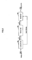
- FIG. 1 is a functional block diagram of an example of an image processing system in an image pickup device to which an embodiment of the present invention is applied.
- the image pickup device also includes an operations unit, an image display unit (monitor), an optical system, and mechanical mechanisms for controlling the shutter speed and adjusting the diaphragm of the lens, although not shown in FIG. 1 .
- the image pickup device is assumed to be used as an in-vehicle camera, although the purpose of the image pickup device is not so limited.
- a control unit 100 controls the operations of the units in the image pickup device in a pipeline-like manner by providing necessary control signals (clocks, horizontal/vertical synchronization signals, etc.) to the units in the image pickup device.
- the control unit 100 includes an MTF correction switching control unit 105, which is described below.
- the MTF correction switching control unit 105 can be provided separately from the control unit 100.
- An image sensor 110 is, for example, a CCD or a CMOS sensor for converting an optical image, which has been taken with the use of an optical system (not shown) having large magnification chromatic aberration and large skew aberration at a wide angle, into electric signals (image signals).
- the image sensor 110 is provided with a color filter of the Bayer array. RGB image data of the Bayer array is sequentially output by a progressive method based on control signals (clocks, horizontal/vertical synchronization signals, etc.) received from the control unit 100.
- An AGC circuit 120 amplifies images signals that are analog signals output from the image sensor 110, to predetermined values. Generally, the gain amount of the AGC circuit 120 is determined to be a suitable value in consideration of the trade-off between the demanded brightness of the screen and noise.
- An A/D converter 130 converts RGB image signals of the Bayer array which are the analog signals amplified at the AGC circuit 120, into digital signals (image data), and sends the resultant digital signals to a Bayer complementary unit 140.
- the image data includes eight bits of data for each of R, G, and B, for example.
- the Bayer complementary unit 140 receives RGB image data of the Bayer array which has been converted into digital signals.
- the Bayer complementary unit 140 performs linear complementation so that image data for all coordinate positions is separately generated for each of the colors of RGB. Then, the Bayer complementary unit 140 sends the image data to a magnification chromatic aberration correction unit 150.
- R 2 , R 4 , R 6 , R 8 , R 0 are obtained by the following formulae.
- R 2 R 1 + R 3 / 2
- R 4 R 3 + R 5 / 2
- R 6 R 5 + R 7 / 2
- R 8 R 1 + R 7 / 2
- R 0 R 1 + R 3 + R 5 + R 7 / 4
- the method for obtaining B 2 , B 4 , B 6 , B 8 , Bo is the same as that used for R 2 , R 4 , R 6 , R 8 , R 0 , and is thus not further described.
- an image sensor having a color filter of the Bayer array In the present embodiment, a description is given of an image sensor having a color filter of the Bayer array. However, the same effects can be achieved with an image sensor having a color filter of another array such as a CMYG array or an RGB+Ir (infrared) array. Such an image sensor having a color filter array of four colors is more effective than an image sensor having a color filter array of three colors like RGB, because a memory of low latency or a four port RAM would be required for the magnification chromatic aberration correction.
- the magnification chromatic aberration correction unit 150 receives the RGB image data which has undergone Bayer complementation. At the magnification chromatic aberration correction unit 150, coordinate conversion (magnification chromatic aberration coordinate conversion) is separately performed for each of the color components of R, G, and B with the use of a predetermined polynomial equation. The magnification chromatic aberration correction unit 150 outputs the RGB image data that has undergone magnification chromatic aberration correction. Magnification chromatic aberration is different for each of the color components, but the extent of aberration is small. Thus, for the coordinate conversion in magnification chromatic aberration correction, a memory having low capacity and low latency or a memory having low capacity and plural ports (SRAM, etc.) can be used. An MTF correction unit 160 and the output side of the magnification chromatic aberration correction unit 150 are connected to a switch circuit 170.
- the MTF correction unit 160 receives the RGB image data that has undergone magnification chromatic aberration correction. At the MTF correction unit 160, an MTF correction process is performed on the RGB image data with the use of an FIR filter. The MTF correction unit 160 outputs the RGB image data which has undergone MTF correction.
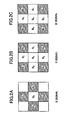
- FIG. 3 is a schematic diagram of the MTF correction unit 160.
- a converter 162 converts the RGB image data into YCbCr pixel data by the following formulae.
- Cb - 0.169 ⁇ R - 0.332 ⁇ G + 0.500 ⁇ B
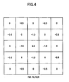
- An FIR filter (5 ⁇ 5 filter) 164 receives only the Y luminance signals among the YCbCr signals, and performs a predetermined MTF correction process on the Y luminance signals.
- FIG. 4 illustrates an example of the FIR filter.
- the MTF correction unit is preferably provided at a stage after the magnification chromatic aberration correction and before the skew aberration correction.
- An inverter 166 receives the CbCr signals and the Y signals that have undergone MTF correction, inserts these signals by the following formulae, and outputs the RGB image data.
- B Y + 1.772 ⁇ Cb
- the switch circuit 170 is usually connected to the MTF correction unit 160 to receive the RGB image data that has undergone MTF correction from the NTF correction unit 160, and to output this RGB image data to a skew aberration correction unit 180 provided at a subseguent stage.
- the switch circuit 170 receives a signal for switching off the MTF correction from the MTF correction switching control unit 105 of the control unit 100, the switch circuit 170 is disconnected from the MTF correction unit 160 and is connected to the magnification chromatic aberration correction unit 150.
- the switch circuit 170 receives the RGB image data from the magnification chromatic aberration correction unit 150 and directly outputs this RGB image data to the skew aberration correction unit 180.
- the skew aberration correction unit 180 receives the RGB image data that has undergone MTF correction from the MTF correction unit 160, or the RGB image data that has not undergone MTF correction from the magnification chromatic aberration correction unit 150.
- the skew aberration correction unit 180 performs the same coordinate conversion (skew aberration coordinate conversion) on each of the color components of RGB with the use of a predetermined polynomial equation, and outputs the RGB image data that has undergone skew aberration correction.
- the skew aberration is larger than the magnification chromatic aberration; however, the extent of skew aberration is the same for all of the color components of RGB.
- a gamma correction unit 190 receives the RGB image data output from the skew aberration correction unit 180, performs a predetermined gamma correction process with the use of look-up tables provided for each of RGB, and outputs the RGB image data that has undergone gamma correction to a display device (not shown).
- the above describes the overall operation of the image pickup device shown in FIG. 1 according to an embodiment of the present invention.
- the following describes the MTF correction switching control unit 105 which is the main element of an embodiment of the present invention.
- the MTF correction switching control unit 105 of the control unit 100 determines that the illuminance is low based on information directly or indirectly indicating the illuminance of the surrounding atmosphere, the MTF correction switching control unit 105 sends a switching signal for turning off the MTF correction to the switch circuit 170.
- the switch circuit 170 bypasses the MTF correction unit 160. Accordingly, when the illuminance is low, MTF correction is not performed, thus reducing the noise in the reproduced image.
- the MTF correction switching control unit 105 sends a switching signal for turning off the MTF correction to the switch circuit 170, the gain of the AGC circuit 120 is increased at the same time. Accordingly, the sensitivity of the reproduced image is increased.
- the image pickup device is used as an in-vehicle camera.
- the MFT switching control unit 105 determines that the illuminance is low when the small lights or the tail lights are switched on.
- an MTF correction process is not performed.
- the illuminance is determined based on an output value from an image sensor, an output value from an illuminance sensor provided separately; the time indicated by a built-in clock, or whether small lights or tail lights are switched on.
Landscapes
- Engineering & Computer Science (AREA)
- Multimedia (AREA)
- Signal Processing (AREA)
- Studio Devices (AREA)
- Color Television Image Signal Generators (AREA)
- Closed-Circuit Television Systems (AREA)
Claims (2)
- Dispositif de capture d'image pour une utilisation dans un véhicule sous forme de camera embarquée, comprenant :un système optique ;un détecteur d'image (110) ;un circuit de commande automatique de gain CAG (120) ;une unité de traitement d'image (160) configurée pour mettre en oeuvre au moins un procédé de correction par fonction de transfert de modulation FTM ; etune unité de commande (105) configurée pour commander l'unité de traitement d'image de manière à ce qu'elle ne mette pas en oeuvre le procédé de correction FTM dans le cas où l'unité de commande (105) détermine que l'éclairement lumineux ambiant est faible, en se basant sur des informations qui indiquent directement ou indirectement l'éclairement lumineux, et configurée pour déterminer que l'éclairement lumineux est faible lorsque des veilleuses ou des feux arrière du véhicule sont allumés.
- Dispositif de capture d'image selon la revendication 1, dans lequel l'unité de commande (105) est en outre configurée pour augmenter le gain du circuit CAG dans le cas où l'éclairement lumineux est déterminé comme étant faible.
Applications Claiming Priority (1)
| Application Number | Priority Date | Filing Date | Title |
|---|---|---|---|
| JP2008033586A JP5152491B2 (ja) | 2008-02-14 | 2008-02-14 | 画像撮像装置 |
Publications (3)
| Publication Number | Publication Date |
|---|---|
| EP2091237A2 EP2091237A2 (fr) | 2009-08-19 |
| EP2091237A3 EP2091237A3 (fr) | 2010-06-02 |
| EP2091237B1 true EP2091237B1 (fr) | 2014-11-05 |
Family
ID=40786627
Family Applications (1)
| Application Number | Title | Priority Date | Filing Date |
|---|---|---|---|
| EP09250341.6A Ceased EP2091237B1 (fr) | 2008-02-14 | 2009-02-11 | Dispositif de capture d'images |
Country Status (4)
| Country | Link |
|---|---|
| US (1) | US8089529B2 (fr) |
| EP (1) | EP2091237B1 (fr) |
| JP (1) | JP5152491B2 (fr) |
| CN (1) | CN101510955B (fr) |
Families Citing this family (5)
| Publication number | Priority date | Publication date | Assignee | Title |
|---|---|---|---|---|
| TWI377508B (en) * | 2008-01-17 | 2012-11-21 | Asia Optical Co Inc | Image pickup methods and image pickup systems using the same |
| JP5078147B2 (ja) * | 2008-03-04 | 2012-11-21 | 株式会社リコー | 画像処理装置及び画像撮像装置 |
| US8237823B2 (en) | 2008-11-06 | 2012-08-07 | Samsung Electronics Co., Ltd. | Method and apparatus for canceling chromatic aberration |
| TWI395469B (zh) * | 2010-03-26 | 2013-05-01 | Primax Electronics Ltd | 影像擷取方法與應用該方法之影像擷取裝置 |
| JP5601000B2 (ja) | 2010-03-31 | 2014-10-08 | 株式会社リコー | 撮像装置 |
Citations (1)
| Publication number | Priority date | Publication date | Assignee | Title |
|---|---|---|---|---|
| WO1999014943A1 (fr) * | 1997-09-16 | 1999-03-25 | Gentex Corporation | Circuit de commande pour capteurs d'ensemble d'images et commande automatique d'eclairage |
Family Cites Families (18)
| Publication number | Priority date | Publication date | Assignee | Title |
|---|---|---|---|---|
| JPH04123946A (ja) * | 1990-09-17 | 1992-04-23 | Toshiba Corp | 車載用監視カメラ装置 |
| JPH0686064A (ja) * | 1992-09-03 | 1994-03-25 | Ricoh Co Ltd | ビデオ信号2値化装置 |
| JP3386203B2 (ja) | 1993-05-07 | 2003-03-17 | 株式会社リコー | 画情報の処理方法及び画情報処理装置 |
| JPH09298683A (ja) | 1996-04-26 | 1997-11-18 | Sony Corp | 映像信号処理方法及び映像信号処理装置 |
| JPH10327321A (ja) | 1997-05-23 | 1998-12-08 | Canon Inc | 画像読み取り装置及び画像読み取り方法 |
| JP3411791B2 (ja) | 1997-07-10 | 2003-06-03 | ペンタックス株式会社 | 画像読取装置 |
| JP2001275029A (ja) * | 2000-03-28 | 2001-10-05 | Minolta Co Ltd | デジタルカメラ、その画像信号処理方法及び記録媒体 |
| JP2003069829A (ja) | 2001-08-24 | 2003-03-07 | Canon Inc | 画像処理装置及びその方法 |
| JP2003315650A (ja) * | 2002-04-26 | 2003-11-06 | Olympus Optical Co Ltd | 光学装置 |
| JP2005130297A (ja) * | 2003-10-24 | 2005-05-19 | Olympus Corp | 信号処理システム、信号処理方法、信号処理プログラム |
| JP2005260640A (ja) * | 2004-03-12 | 2005-09-22 | Matsushita Electric Ind Co Ltd | 撮像処理装置 |
| JP2005303595A (ja) * | 2004-04-09 | 2005-10-27 | Konica Minolta Photo Imaging Inc | 撮像装置 |
| JP4577565B2 (ja) * | 2005-03-03 | 2010-11-10 | ソニー株式会社 | 画像処理方法、画像処理装置、プログラム、および撮影装置 |
| JP2006318213A (ja) * | 2005-05-12 | 2006-11-24 | Sharp Corp | 画像処理回路及び画像処理方法 |
| JP4596986B2 (ja) | 2005-06-07 | 2010-12-15 | オリンパス株式会社 | 画像撮像装置 |
| KR20070070822A (ko) | 2005-12-29 | 2007-07-04 | 주식회사 팬택앤큐리텔 | 촬영 장치 및 카메라 제어 방법 |
| JP2007194775A (ja) | 2006-01-18 | 2007-08-02 | Sanyo Electric Co Ltd | ディテイルエンハンサー |
| JP2008033586A (ja) | 2006-07-28 | 2008-02-14 | Hitachi Ltd | セキュリティ対策状況監視システムにおけるセキュリティポリシーの自動更新方法 |
-
2008
- 2008-02-14 JP JP2008033586A patent/JP5152491B2/ja not_active Expired - Fee Related
-
2009
- 2009-02-04 CN CN200910004899.3A patent/CN101510955B/zh not_active Expired - Fee Related
- 2009-02-05 US US12/320,822 patent/US8089529B2/en active Active
- 2009-02-11 EP EP09250341.6A patent/EP2091237B1/fr not_active Ceased
Patent Citations (1)
| Publication number | Priority date | Publication date | Assignee | Title |
|---|---|---|---|---|
| WO1999014943A1 (fr) * | 1997-09-16 | 1999-03-25 | Gentex Corporation | Circuit de commande pour capteurs d'ensemble d'images et commande automatique d'eclairage |
Also Published As
| Publication number | Publication date |
|---|---|
| CN101510955A (zh) | 2009-08-19 |
| EP2091237A3 (fr) | 2010-06-02 |
| US20090207276A1 (en) | 2009-08-20 |
| CN101510955B (zh) | 2012-12-12 |
| JP5152491B2 (ja) | 2013-02-27 |
| US8089529B2 (en) | 2012-01-03 |
| JP2009194651A (ja) | 2009-08-27 |
| EP2091237A2 (fr) | 2009-08-19 |
Similar Documents
| Publication | Publication Date | Title |
|---|---|---|
| EP2104363B1 (fr) | Dispositif de capture d'images | |
| EP2099229B1 (fr) | Appareil et procédé de traitement d'image | |
| EP2088773B1 (fr) | Procédé de conversion de progressif à entrelaçage, appareil de traitement d'images, appareil d'imagerie | |
| JP6319340B2 (ja) | 動画撮像装置 | |
| US9936172B2 (en) | Signal processing device, signal processing method, and signal processing program for performing color reproduction of an image | |
| EP2133238B1 (fr) | Appareil d'imagerie et procédé de correction d'images | |
| JP5112238B2 (ja) | 撮像装置、設定値変更方法およびプログラム | |
| EP2091237B1 (fr) | Dispositif de capture d'images | |
| JP2000244823A (ja) | 撮像素子の欠陥画素補正装置 | |
| KR20030005009A (ko) | 화상 데이터의 수정 방법 및 화상 신호 처리 장치 | |
| EP2214136B1 (fr) | Procédé et programme de contrôle d'appareil de capture d'images | |
| JP2006140791A (ja) | デジタルカメラとその信号処理方法及び信号処理装置 | |
| JP4874752B2 (ja) | デジタルカメラ | |
| US20070285529A1 (en) | Image input device, imaging module and solid-state imaging apparatus | |
| KR20100082452A (ko) | 이미지 신호 처리 장치 및 방법 | |
| JP2006060744A (ja) | ノイズリダクション装置 | |
| JP4235408B2 (ja) | ノイズ低減回路及び撮像装置 | |
| JP4880375B2 (ja) | 画像信号処理装置及び画像信号処理方法 | |
| JP2007043312A (ja) | 撮影装置 | |
| KR100999885B1 (ko) | 이미지 신호 처리 장치, 이미지 신호 처리 장치의 색 노이즈 저감 방법 및 색 노이즈 저감 방법이 기록된 기록 매체 | |
| JP2004007160A (ja) | シェーディング補正装置 | |
| JP2006303774A (ja) | 撮像装置 | |
| JP6536032B2 (ja) | 車載カメラ |
Legal Events
| Date | Code | Title | Description |
|---|---|---|---|
| PUAI | Public reference made under article 153(3) epc to a published international application that has entered the european phase |
Free format text: ORIGINAL CODE: 0009012 |
|
| 17P | Request for examination filed |
Effective date: 20090223 |
|
| AK | Designated contracting states |
Kind code of ref document: A2 Designated state(s): AT BE BG CH CY CZ DE DK EE ES FI FR GB GR HR HU IE IS IT LI LT LU LV MC MK MT NL NO PL PT RO SE SI SK TR |
|
| AX | Request for extension of the european patent |
Extension state: AL BA RS |
|
| PUAL | Search report despatched |
Free format text: ORIGINAL CODE: 0009013 |
|
| AK | Designated contracting states |
Kind code of ref document: A3 Designated state(s): AT BE BG CH CY CZ DE DK EE ES FI FR GB GR HR HU IE IS IT LI LT LU LV MC MK MT NL NO PL PT RO SE SI SK TR |
|
| AX | Request for extension of the european patent |
Extension state: AL BA RS |
|
| AKX | Designation fees paid |
Designated state(s): DE FR GB |
|
| 17Q | First examination report despatched |
Effective date: 20120511 |
|
| GRAP | Despatch of communication of intention to grant a patent |
Free format text: ORIGINAL CODE: EPIDOSNIGR1 |
|
| INTG | Intention to grant announced |
Effective date: 20140527 |
|
| GRAS | Grant fee paid |
Free format text: ORIGINAL CODE: EPIDOSNIGR3 |
|
| GRAA | (expected) grant |
Free format text: ORIGINAL CODE: 0009210 |
|
| AK | Designated contracting states |
Kind code of ref document: B1 Designated state(s): DE FR GB |
|
| REG | Reference to a national code |
Ref country code: GB Ref legal event code: FG4D |
|
| REG | Reference to a national code |
Ref country code: DE Ref legal event code: R096 Ref document number: 602009027541 Country of ref document: DE Effective date: 20141218 |
|
| REG | Reference to a national code |
Ref country code: DE Ref legal event code: R097 Ref document number: 602009027541 Country of ref document: DE |
|
| PLBE | No opposition filed within time limit |
Free format text: ORIGINAL CODE: 0009261 |
|
| STAA | Information on the status of an ep patent application or granted ep patent |
Free format text: STATUS: NO OPPOSITION FILED WITHIN TIME LIMIT |
|
| 26N | No opposition filed |
Effective date: 20150806 |
|
| REG | Reference to a national code |
Ref country code: FR Ref legal event code: PLFP Year of fee payment: 8 |
|
| REG | Reference to a national code |
Ref country code: FR Ref legal event code: PLFP Year of fee payment: 9 |
|
| REG | Reference to a national code |
Ref country code: FR Ref legal event code: PLFP Year of fee payment: 10 |
|
| PGFP | Annual fee paid to national office [announced via postgrant information from national office to epo] |
Ref country code: DE Payment date: 20200219 Year of fee payment: 12 Ref country code: GB Payment date: 20200219 Year of fee payment: 12 |
|
| PGFP | Annual fee paid to national office [announced via postgrant information from national office to epo] |
Ref country code: FR Payment date: 20200219 Year of fee payment: 12 |
|
| REG | Reference to a national code |
Ref country code: DE Ref legal event code: R119 Ref document number: 602009027541 Country of ref document: DE |
|
| GBPC | Gb: european patent ceased through non-payment of renewal fee |
Effective date: 20210211 |
|
| PG25 | Lapsed in a contracting state [announced via postgrant information from national office to epo] |
Ref country code: DE Free format text: LAPSE BECAUSE OF NON-PAYMENT OF DUE FEES Effective date: 20210901 Ref country code: GB Free format text: LAPSE BECAUSE OF NON-PAYMENT OF DUE FEES Effective date: 20210211 Ref country code: FR Free format text: LAPSE BECAUSE OF NON-PAYMENT OF DUE FEES Effective date: 20210228 |