EP2089905B1 - Silicide strapping in imager transfer gate device - Google Patents
Silicide strapping in imager transfer gate device Download PDFInfo
- Publication number
- EP2089905B1 EP2089905B1 EP07867600.4A EP07867600A EP2089905B1 EP 2089905 B1 EP2089905 B1 EP 2089905B1 EP 07867600 A EP07867600 A EP 07867600A EP 2089905 B1 EP2089905 B1 EP 2089905B1
- Authority
- EP
- European Patent Office
- Prior art keywords
- conductivity type
- type material
- gate
- silicide
- transfer gate
- Prior art date
- Legal status (The legal status is an assumption and is not a legal conclusion. Google has not performed a legal analysis and makes no representation as to the accuracy of the status listed.)
- Active
Links
Images


Classifications
-
- H—ELECTRICITY
- H10—SEMICONDUCTOR DEVICES; ELECTRIC SOLID-STATE DEVICES NOT OTHERWISE PROVIDED FOR
- H10F—INORGANIC SEMICONDUCTOR DEVICES SENSITIVE TO INFRARED RADIATION, LIGHT, ELECTROMAGNETIC RADIATION OF SHORTER WAVELENGTH OR CORPUSCULAR RADIATION
- H10F39/00—Integrated devices, or assemblies of multiple devices, comprising at least one element covered by group H10F30/00, e.g. radiation detectors comprising photodiode arrays
- H10F39/10—Integrated devices
- H10F39/12—Image sensors
-
- H—ELECTRICITY
- H10—SEMICONDUCTOR DEVICES; ELECTRIC SOLID-STATE DEVICES NOT OTHERWISE PROVIDED FOR
- H10F—INORGANIC SEMICONDUCTOR DEVICES SENSITIVE TO INFRARED RADIATION, LIGHT, ELECTROMAGNETIC RADIATION OF SHORTER WAVELENGTH OR CORPUSCULAR RADIATION
- H10F39/00—Integrated devices, or assemblies of multiple devices, comprising at least one element covered by group H10F30/00, e.g. radiation detectors comprising photodiode arrays
- H10F39/80—Constructional details of image sensors
- H10F39/803—Pixels having integrated switching, control, storage or amplification elements
-
- H—ELECTRICITY
- H10—SEMICONDUCTOR DEVICES; ELECTRIC SOLID-STATE DEVICES NOT OTHERWISE PROVIDED FOR
- H10F—INORGANIC SEMICONDUCTOR DEVICES SENSITIVE TO INFRARED RADIATION, LIGHT, ELECTROMAGNETIC RADIATION OF SHORTER WAVELENGTH OR CORPUSCULAR RADIATION
- H10F39/00—Integrated devices, or assemblies of multiple devices, comprising at least one element covered by group H10F30/00, e.g. radiation detectors comprising photodiode arrays
- H10F39/011—Manufacture or treatment of image sensors covered by group H10F39/12
- H10F39/014—Manufacture or treatment of image sensors covered by group H10F39/12 of CMOS image sensors
-
- H—ELECTRICITY
- H10—SEMICONDUCTOR DEVICES; ELECTRIC SOLID-STATE DEVICES NOT OTHERWISE PROVIDED FOR
- H10F—INORGANIC SEMICONDUCTOR DEVICES SENSITIVE TO INFRARED RADIATION, LIGHT, ELECTROMAGNETIC RADIATION OF SHORTER WAVELENGTH OR CORPUSCULAR RADIATION
- H10F39/00—Integrated devices, or assemblies of multiple devices, comprising at least one element covered by group H10F30/00, e.g. radiation detectors comprising photodiode arrays
- H10F39/10—Integrated devices
- H10F39/12—Image sensors
- H10F39/18—Complementary metal-oxide-semiconductor [CMOS] image sensors; Photodiode array image sensors
Definitions
- the present invention relates to semiconductor optical image sensors, and particularly, to a novel CMOS (complementary metal oxide semiconductor) image sensor cell structure exhibiting reduced lag, higher capacity and lower dark current.
- CMOS complementary metal oxide semiconductor
- CMOS image sensors comprise an array of CMOS Active Pixel Sensor (APS) cells, which are used to collect light energy and convert it,into readable electrical signals.
- Each APS cell comprises a photosensitive element, such as a photodiode, photogate, or photoconductor overlying a doped region of a substrate for accumulating photo-generated charge in an underlying portion thereof.
- a read-out circuit is connected to each pixel cell and often includes a diffusion region for receiving charge from the photosensitive element, when read-out. Typically, this is accomplished by a transistor device having a gate electrically connected to the floating diffusion region.
- the imager may also include a transistor, having a transfer gate, for transferring charge from the photosensitive element across a channel to the floating diffusion region, and a transistor for resetting the floating diffusion region to a predetermined charge level prior to charge transfer.
- a typical CMOS APS cell 10 includes a pinned photodiode 20 having a pinning layer 18 doped p -type and, an underlying lightly doped n-type region 17.
- the pinned diode 20 is formed on top of a p-type substrate 15 or a p-type epitaxial layer or p-well surface layer having a lower p-type concentration than the diode pinning layer 18.
- the surface doped p -type pinning layer 18 is in electrical contact with the substrate 15 (or p-type epitaxial layer or p-well surface layer).
- the photodiode 20 thus has two p-type regions 18 and 15 having a same potential so that the n-type doped region 17 is fully depleted at a pinning voltage (Vp). That is, the surface pinning layer 18 is in electrical contact to the substrate.
- the pinned photodiode is termed "pinned" because the potential in the photodiode is pinned to a constant value, Vp, when the photodiode is fully depleted.
- This pinned photodiode configuration improves the device performance by decreasing dark current (current output by a pixel in a dark environment).
- the pinned photodiode configuration may cause image lag due to the incomplete transfer of charge from the photodiode to the floating node.
- the transfer gate 25 When the transfer gate 25 is operated, i.e., turned on by applying a voltage to the transfer gate 70 comprising, for example, an n-type doped polysilicon layer 70 over a thin dielectric layer 60, the photo-generated charge 24 is transferred from the charge accumulating doped n-type doped region 17 via a transfer device channel 16 to a floating diffusion region 30, e.g., a floating "node" doped n+ type.
- Fig. 2 depicts a further prior art CMOS APS cell 10' having incorporated a gate 25' having a portion that is p-type material 70a and a portion that is n-type 70b.
- the n-type portion 70b of the gate has a lower Vt and the p-type portion 70a of the gate has a higher Vt.
- the transfer gate has a built in field pulling electrons from the photodiode to the floating diffusion.
- silicide contact regions not shown
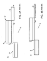
- Fig. 3A depicts a CMOS imager 12 having a silicide layer blocked from the photodiode surface since silicide blocks light while a silicide layer 80 formed over the transfer gate polysilicon and floating diffusion remain.
- Fig. 3B illustrates the CMOS imager 12 of Fig. 3A having silicide layers 80 removed from the gate poly and floating diffusion for even lower leakage behavior.
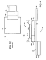
- Fig. 3C illustrates a top plan view of the CMOS imager 10' of Fig. 2 having silicide surface layers removed from the photodiode 20, gate poly regions 70a, 70b and floating diffusion node 30.
- each CMOS APS cell gate polysilicon formed with the built-in diode within the gate prevents the entire gate from being contacted. That is, a contact which only connects either the n-type or p-type side of the polysilicon gate will not be adequately connected to the other polarity of the gate poly layer. This results in a time dependent voltage on the uncontacted portion of the gate. That is, if a contact is made to the n-type part of the gate, the p-type part floats; likewise, if contact is made to the p-type side of the gate, the n-type part floats. If a contact is formed directly over the boundary edge, contact overlay allows it to contact only one side statistically.
- US patent application publication number US2004/262651 A1 discloses a method of forming a pixel cell and the resultant pixel cell which includes a photo-conversion device formed at a surface of the substrate and a transistor adjacent to the photo-conversion device.
- the transistor comprises a gate overlying a channel region.
- the gate comprises at least one gate region having a work-function greater than a work-function of n+ polysilicon.
- the channel region comprises respective portions below each gate region.
- a dopant concentration in at least one portion of the channel region is determined at least in part by the work-function of the respective gate region.
- European patent application publication number EP1 139 428 A discloses a solid state imaging device having a photodiode and a MOSFET and method of manufacturing the same.
- the readout gate electrode is selectively formed on a silicon substrate.
- An N-type drain region is formed at one end of the readout gate electrode and an N-type signal storage region is formed at the other end thereof.
- a P + -type surface shield region is selectively epitaxial-grown on the signal storage region, and a silicide block layer is formed on the surface shield region to cover at least part of the signal storage region.
- a Ti silicide film is selective epitaxial-grown on the drain region.
- the invention provides an active pixel sensor (APS) cell structure as set out in claim 1 and a method for forming this active pixel sensor (APS) all structure according to claim 10.
- APS active pixel sensor
- the invention relates generally to improved semiconductor imaging devices and in particular to an imaging device which can be fabricated using a standard CMOS process.
- the interconnect layer comprises a silicide and is formed in physical contact with at least a portion of the p-type region and a portion of the n-type region of a polysilicon transfer gate.
- the silicide layer is over just a portion of the poly gate width and silicide is not formed on the diffusions (i.e. photodiode and floating diffusion).
- the CMOS imager includes a transfer gate device having two workfunctions (n-type and p-type gate poly) and a silicide strap cooperatively exhibit a high barrier at the photodiode for dark current while a low barrier is provided at the floating diffusion for low lag performance.
- the silicide strap prevents the diodic behavior from allowing one or the other side of the gate to float to an indeterminate voltage.
- the photosensing device comprises a photodiode comprising: a collection well of a second conductivity type material formed below the substrate surface; and, a pinning layer of the first conductivity type material formed atop the collection well at the substrate surface.
- the substrate, pinning layer of the first conductivity type material, and the first doped region of the dual workfunction gate conductor layer of the transfer gate device includes p-type dopant material, e.g., Boron or Indium.
- the collection well of the second conductivity type material, the floating diffusion region of second conductivity type material, and the second doped region of the dual workfunction gate conductor layer of the transfer gate includes n-type dopant material, e.g., Phosphorus, Arsenic or Antimony.
- the silicide structure comprises a silicide of Ti, Ta, W, Co, Ni, Pt, Pd or alloys thereof.
- the silicide structure formed over the dual workfunction gate conductor layer for electrically coupling the first doped region of first conductivity type material and the second doped region of second conductivity type material of the transfer gate device is smaller in area dimension than an area dimension of the dual workfunction gate conductor layer.
- the silicide structure formed over the dual workfunction gate conductor layer for electrically coupling the first doped region of first conductivity type material and the second doped region of second conductivity type material of the transfer gate device is reduced only in length dimension than a length of the dual workfunction gate conductor layer.
- teachings of the invention may be applicable for devices of both polarities, i.e., n type photodiodes and p type pinning layers and nFETS, as well as to p type photodiodes, and n type pinning layers with pFETs.
- CMOS complementary metal oxide silicon type electrical components such as transistors which are associated with the pixel, but typically not in the pixel, and which are formed when the source/drain of a transistor is of one dopant type and its mated transistor is of the opposite dopant type.
- CMOS devices include some advantages one of which is it consumes less power.
- Fig. 4 illustrates, through a cross-sectional view, a back end of line CMOS imager APS 100 including photosensing device, e.g., photodiode 200, and silicon-containing, e.g., polysilicon, transfer gate 125 according to a first embodiment of the invention.
- the polysilicon transfer gate 125 includes an anodic (p-type doped) region and abutting cathodic (n-type doped) region forming a diode.
- the polysilicon transfer gate 125 comprises a Schottky diode.
- a conductive structure e.g., a partial silicide "strap" 190, is formed on the surface of the poly gate having p-type 175a and n-type 175b portions for improved gate barrier ac characteristics as will be described in greater detail herein below.
- the partial silicide strap layer 190 electrically connects the p-type doped 175a and n-type doped 175b portions of the polysilicon gate 125.
- the partial silicide "strap" layer 190 has edges formed at a distance from the boundary of the gate, i.e., the silicide strap 190 is inset a distance, e.g., distances d 1 and d 2 , from respective edges 171, 172 of the poly gate layer.
- the inset distances d 1 and d 2 of the formed silicide strap are not required to be equal, i.e., the strap is formed to lie over just a portion of the poly width, as long as the silicide strap 190 electrically shorts the p-type portion 175a to the n-type portion 175b.
- the silicide strap 190 is formed atop a portion of the poly width. It is understood that in preferred embodiments, the silicide strap 190 is kept off the diffusion 130.
- the device 100 is formed on a substrate 15 which may be a bulk semiconductor including, for example, Si, SiGe, SiC, SiGeC, GaAs, InP, InAs and other semiconductors, or layered semiconductors such as silicon-on-insulators (SOI), SiC-on-insulator (SiCOI) or silicon germanium-on-insulators (SGOI).
- SOI silicon-on-insulators
- SiCOI SiC-on-insulator
- SGOI silicon germanium-on-insulators
- substrate 15 is a Si-containing semiconductor substrate of a first conductivity type, e.g., lightly doped with p-type dopant material such as boron or indium (beryllium or magnesium for a III-V semiconductor), to a standard concentration ranging between, e.g., 1x10 14 to 1x10 16 cm -3 .
- p-type dopant material such as boron or indium (beryllium or magnesium for a III-V semiconductor
- dielectric material layer 60 is formed by standard deposition/growth techniques atop the substrate 15 that will form the eventual transfer gate dielectric.
- the dielectric layer may be formed to a thickness ranging between 40 ⁇ to 100 ⁇ , for example, and may comprise suitable gate dielectric materials including but not limited to: an oxide (e.g., SiO 2 ), a nitride (e.g., silicon nitride) an oxynitride (e.g, Si oxynitride), N 2 O, NO, ZrO 2 , or other like materials.
- the gate dielectric 60 is comprised of an oxide such as, for example, SiO 2 , HfO 2 , ZrO 2 , Al 2 O 3 , TiO 2 , La 2 O 3 , SrTiO 3 , LaAlO 3 , and mixtures thereof.
- the dielectric layer 60 is formed on the surface of the Si-containing semiconductor substrate 15 using conventional thermal oxidation or by a suitable deposition process such as chemical vapor deposition, plasma-assisted chemical vapor deposition, atomic layer deposition (ALD), evaporation, reactive sputtering, chemical solution deposition and other like deposition processes.
- the gate dielectric 16 may also be formed utilizing any combination of the above processes. Although it is not shown, it is understood that the dielectric layer may comprise a stack of dielectric materials.
- a Silicon-containing layer e.g., polycrystalline silicon
- CVD chemical vapor deposition
- sputtering a physical vapor deposition
- plating evaporation
- other like deposition processes e.g., a low pressure CVD
- the polysilicon layer may be formed to a thickness ranging between about 1k ⁇ to 2k ⁇ but may be outside this range.
- the Silicon-containing layer may comprise a stack of polysilicon layers.
- a subsequent mask deposition process that covers a portion of the transfer gate structure and ion implantation process is performed to implant dopant material of a second conductivity type, e.g., n -type dopant material, such as phosphorus, arsenic or antimony, into the polysilicon layer to form n -type doped gate poly portion 175b.
- dopant material of a second conductivity type e.g., n -type dopant material, such as phosphorus, arsenic or antimony
- the n-type dopant material may be implanted to achieve a dosing concentration ranging between 1x10 17 cm -3 to 1x10 20 cm -3 .
- an ion implantation process is performed to implant dopant material of a first conductivity type, e.g., p -type dopant material, such as boron or gallium or indium into the polysilicon layer to form p -type doped gate poly portion 175a as shown in Fig. 4 .
- the p-type dopant material may be implanted to achieve a dosing concentration ranging between 1x10 17 cm -3 to 1x10 20 cm -3 in the gate poly.
- the doping of the polysilicon may be achieved using implants already present in the process by appropriate use of those implant masks at the same time those implants are being performed elsewhere in the chip. (One example would be the source drain implants and masks, but others are also possible.)
- gate sidewall spacers may be formed at either side of the transfer gate by conventional deposition processes well known in the art, and may comprise any conventional oxide or nitride (e.g., Si 3 N 4 ) or oxide/nitride which are then etched by RIE or another like etch process.
- the thickness of spacers may vary, but typically they have a thickness of from about 5 nm to about 150 nm.
- a next step is performed to provide the photodiode pinning region 180.
- This step comprises forming a photoresist layer (not shown) patterning, and creating an ion implantation mask according to techniques known in the art to form a mask edge approximately coincident with the gate edge or as close as possible given alignment tolerances, to provide an opening to an area between an edge of the gate and a formed isolation region, e.g., STI region (not shown), where the charge accumulation region of the photodiode is to be formed.
- This opening permits the implantation of ions of p-type dopant material, e.g., such as boron, at a concentration sufficient to form the p -type dopant pinning region 180 as shown in Figure 4 .
- This pinning region 180 may be formed up to the edge of a spacer (not shown).
- the active p -type dopant material is then ion implanted at dosing concentrations ranging between 1x10 17 and 1x10 19 cm -3 .
- the p-type pinning photodiode surface layer 180 may be formed by other known techniques.
- the n-type dopant material is implanted at higher energy levels to form the n-type doped region 170 of the photodiode 190 as shown in Figure 4 .
- the active n-type dopant material may be ion implanted at dosing concentrations ranging between 1x10 16 and 1x10 18 cm -3 .
- the photosensitive charge storage region 170 for collecting photo-generated electrons may be formed by multiple implants to tailor the profile of the n-type region 170.
- an additional step of forming an n-type floating diffusion region 130 at the other side of the transfer gate comprises forming a photoresist layer and patterning and etching an ion implantation mask according to techniques known in the art to form a mask edge approximately coincident with the gate edge or as close as possible given alignment tolerances, to provide an opening allowing the implantation of n -type dopant material, such as phosphorus, arsenic or antimony, at a concentration sufficient to form the n+ -type doped floating diffusion region 130 as shown in Figure 4 or, up to the edge of a gate sidewall spacer (not shown).
- n -type dopant material such as phosphorus, arsenic or antimony
- a salicide process is then performed to consume the polysilicon gate 125 to form the metal silicide strap 190 according to the invention, as shown in Figs.5A-5D .
- the lithography step includes applying a photoresist to the upper surface of the dielectric cap layer, exposing the photoresist to a desired pattern of radiation and developing the exposed photoresist utilizing a conventional resist developer.
- the pattern in the photoresist is then transferred to the dielectric cap layer utilizing one or more dry etching steps leaving exposed the underlying polysilicon gate layer and, particularly, opening up a window in the dielectric cap layer to expose adjacent portions of both doped regions 175a,b in the exposed underlying polysilicon layer.
- the desired pattern is the area and dimension of the silicide strap to be formed such as shown in Figures 5A-5D .
- the photolithographic mask, develop and etch process applied to the overlying cap dielectric (e.g., nitride) layer will result in the exposure region 195 of the underlying polysilicon layer that is inset a distance d1 and d2 from each of the respective gate edges 171, 172 along the length of the gate that will be subject to formation of the silicide contact.
- the patterned photoresist may be removed after the pattern has been transferred into the dielectric cap layer.
- Suitable dry etching processes that can be used in the present invention in forming the patterned gate include, but are not limited to: reactive ion etching, ion beam etching, plasma etching or laser ablation.
- the metal used in forming the silicide strap comprises any metal that is capable of reacting with silicon to form a metal silicide.
- metals include, but are not limited to: Ti, Ta, W, Co, Mo, Ni, Pt, Pd or alloys thereof.
- the metal may be deposited using any conventional deposition process including, for example, sputtering, chemical vapor deposition, a physical vapor deposition (PVD) of the silicide evaporation, chemical solution deposition, plating and the like.
- a thermal anneal process is employed to form a silicide phase in the structure; preferably, the silicide representing the lowest resistivity phase of a metal silicide.
- the anneal is performed utilizing the ambients and temperatures well known in the art that cause the silicide metal to react with the underlying polysilicon to form the metal silicide layer 190 as shown in Fig. 4 .
- the silicide metal may comprise Co noting that CoSi 2 forms using a two step annealing process as known in the art.
- the silicide metal is Ni or Pt; NiSi and PtSi being formed using a single annealing step. Then, a selective wet etch step may be employed to remove any non-reactive silicide metal from the structure.
- the wafer is then annealed at approximately 500° C to about 800°C for approximately 30 seconds in a nitrogen environment to react with the portions of the polysilicon layer 175a,b to form the conductive silicide strap 190.
- Figure 5B illustrates, through a top plan view, the CMOS APS cell 100' formed in accordance with a first variation of the embodiment of the invention shown in Fig, 5A , where a silicide strap 191 is formed utilizing the process described herein that has edges formed an inset distance d 1 ,d 2 from edges of the boundary gate, however, is formed to extend substantially over the whole width of the poly.
- a silicide strap 191 is formed utilizing the process described herein that has edges formed an inset distance d 1 ,d 2 from edges of the boundary gate, however, is formed to extend substantially over the whole width of the poly.
- Figure 5C illustrates, through a top plan view, the CMOS APS cell 100" formed in accordance with a second variation of the embodiment of the invention shown in Fig, 5A , where a silicide strap 192 is formed utilizing the process described herein that has edges formed an inset distance d 1 ,d 2 from edges of the boundary gate, however, extends a short distance of the poly gate.
- a silicide strap 192 is formed utilizing the process described herein that has edges formed an inset distance d 1 ,d 2 from edges of the boundary gate, however, extends a short distance of the poly gate.
- the photolithographic mask, develop and etch process applied to the overlying cap dielectric (e.g., nitride) layer will result in formation of the exposure region 197 of the underlying polysilicon layer that is inset a distance d1 and d2 from each of the respective gate edges 171, 172 along the length of the gate, however extends for only a short distance of the poly gate, for example.
- the overlying cap dielectric e.g., nitride
- the photolithographic mask, develop and etch process applied to the overlying cap dielectric (e.g., nitride) layer will result in formation of the exposure region 198 of the underlying polysilicon layer that is inset a distance from each of the respective gate edges 171, 172 along the length of the gate, and extends for only a short distance of the poly gate, for example, in a region that does not directly overly the device channel region.
- the overlying cap dielectric e.g., nitride
- any conductive structure for electrically shorting the anode 175a and cathode 175b portions of the transfer gate poly may be implemented besides the silicide contact structure as described. However, it is imperative that the photodetection region and the floating diffusion regions be silicide-free.
- a high barrier exists at the photodiode for reducing the dark current leakage, and that a low barrier is present at the floating diffusion for lower lag.
- the silicide strap prevents diodic behavior from allowing one or the other side of the gate to float to an indeterminate voltage.
Landscapes
- Solid State Image Pick-Up Elements (AREA)
- Transforming Light Signals Into Electric Signals (AREA)
Applications Claiming Priority (2)
| Application Number | Priority Date | Filing Date | Title |
|---|---|---|---|
| US11/565,801 US7675097B2 (en) | 2006-12-01 | 2006-12-01 | Silicide strapping in imager transfer gate device |
| PCT/US2007/024684 WO2008069994A2 (en) | 2006-12-01 | 2007-11-30 | Silicide strapping in imager transfer gate device |
Publications (2)
| Publication Number | Publication Date |
|---|---|
| EP2089905A2 EP2089905A2 (en) | 2009-08-19 |
| EP2089905B1 true EP2089905B1 (en) | 2014-01-22 |
Family
ID=39434223
Family Applications (1)
| Application Number | Title | Priority Date | Filing Date |
|---|---|---|---|
| EP07867600.4A Active EP2089905B1 (en) | 2006-12-01 | 2007-11-30 | Silicide strapping in imager transfer gate device |
Country Status (7)
| Country | Link |
|---|---|
| US (2) | US7675097B2 (enExample) |
| EP (1) | EP2089905B1 (enExample) |
| JP (1) | JP5096483B2 (enExample) |
| KR (1) | KR101437194B1 (enExample) |
| CN (1) | CN101281918B (enExample) |
| TW (1) | TWI420659B (enExample) |
| WO (1) | WO2008069994A2 (enExample) |
Families Citing this family (40)
| Publication number | Priority date | Publication date | Assignee | Title |
|---|---|---|---|---|
| CN101536153B (zh) * | 2006-11-06 | 2011-07-20 | Nxp股份有限公司 | 制造fet栅极的方法 |
| US7675097B2 (en) | 2006-12-01 | 2010-03-09 | International Business Machines Corporation | Silicide strapping in imager transfer gate device |
| KR100810423B1 (ko) * | 2006-12-27 | 2008-03-04 | 동부일렉트로닉스 주식회사 | 이미지 센서 및 이미지 센서의 제조 방법 |
| US20080217679A1 (en) * | 2007-03-08 | 2008-09-11 | Macronix International Co., Ltd. | Memory unit structure and operation method thereof |
| KR20090003854A (ko) * | 2007-07-05 | 2009-01-12 | 삼성전자주식회사 | 이미지 센서 및 그 제조 방법 |
| US8110465B2 (en) * | 2007-07-30 | 2012-02-07 | International Business Machines Corporation | Field effect transistor having an asymmetric gate electrode |
| US7741217B2 (en) * | 2007-10-25 | 2010-06-22 | International Business Machines Corporation | Dual workfunction silicide diode |
| US8743247B2 (en) * | 2008-01-14 | 2014-06-03 | International Business Machines Corporation | Low lag transfer gate device |
| US8227844B2 (en) * | 2008-01-14 | 2012-07-24 | International Business Machines Corporation | Low lag transfer gate device |
| TWI347009B (en) * | 2008-02-04 | 2011-08-11 | Jack Kuo | Continuous multigate transistors |
| US20090261393A1 (en) * | 2008-04-18 | 2009-10-22 | United Microelectronics Corp. | Composite transfer gate and fabrication thereof |
| JP5271104B2 (ja) * | 2009-02-13 | 2013-08-21 | 浜松ホトニクス株式会社 | リニアイメージセンサ |
| JP5091886B2 (ja) | 2009-02-13 | 2012-12-05 | 浜松ホトニクス株式会社 | イメージセンサ |
| US20100314667A1 (en) * | 2009-06-11 | 2010-12-16 | Omnivision Technologies, Inc. | Cmos pixel with dual-element transfer gate |
| US9000500B2 (en) | 2009-12-30 | 2015-04-07 | Omnivision Technologies, Inc. | Image sensor with doped transfer gate |
| US8299505B2 (en) | 2011-02-17 | 2012-10-30 | International Business Machines Corporation | Pixel sensor cell with a dual work function gate electode |
| CA2835870A1 (en) | 2011-05-12 | 2012-11-15 | Olive Medical Corporation | Pixel array area optimization using stacking scheme for hybrid image sensor with minimal vertical interconnects |
| US9070784B2 (en) | 2011-07-22 | 2015-06-30 | Taiwan Semiconductor Manufacturing Company, Ltd. | Metal gate structure of a CMOS semiconductor device and method of forming the same |
| JP2013084834A (ja) * | 2011-10-12 | 2013-05-09 | Sharp Corp | 固体撮像素子及び固体撮像素子の製造方法 |
| US9698185B2 (en) * | 2011-10-13 | 2017-07-04 | Omnivision Technologies, Inc. | Partial buried channel transfer device for image sensors |
| US9000527B2 (en) | 2012-05-15 | 2015-04-07 | Apple Inc. | Gate stack with electrical shunt in end portion of gate stack |
| WO2014002365A1 (ja) * | 2012-06-26 | 2014-01-03 | パナソニック株式会社 | 固体撮像装置及びその製造方法 |
| CN104486987A (zh) | 2012-07-26 | 2015-04-01 | 橄榄医疗公司 | 具有最小面积单片式cmos图像传感器的相机系统 |
| US8809925B2 (en) * | 2012-10-11 | 2014-08-19 | Omnivision Technologies, Inc. | Partial buried channel transfer device in image sensors |
| US8912584B2 (en) * | 2012-10-23 | 2014-12-16 | Apple Inc. | PFET polysilicon layer with N-type end cap for electrical shunt |
| WO2014145246A1 (en) | 2013-03-15 | 2014-09-18 | Olive Medical Corporation | Image sensor synchronization without input clock and data transmission clock |
| AU2014233192B2 (en) | 2013-03-15 | 2018-11-22 | DePuy Synthes Products, Inc. | Minimize image sensor I/O and conductor counts in endoscope applications |
| KR102089682B1 (ko) | 2013-07-15 | 2020-03-16 | 삼성전자 주식회사 | 반도체 장치 및 이의 제조 방법 |
| CN103456756A (zh) * | 2013-09-26 | 2013-12-18 | 哈尔滨工程大学 | 一种有源像素结构及其制作方法 |
| US9526468B2 (en) | 2014-09-09 | 2016-12-27 | General Electric Company | Multiple frame acquisition for exposure control in X-ray medical imagers |
| JP6668600B2 (ja) * | 2015-03-19 | 2020-03-18 | セイコーエプソン株式会社 | 固体撮像素子及びその製造方法 |
| US10254389B2 (en) | 2015-11-06 | 2019-04-09 | Artilux Corporation | High-speed light sensing apparatus |
| US10418407B2 (en) | 2015-11-06 | 2019-09-17 | Artilux, Inc. | High-speed light sensing apparatus III |
| TWI724164B (zh) * | 2017-05-05 | 2021-04-11 | 聯華電子股份有限公司 | 半導體元件及其製作方法 |
| US11393867B2 (en) * | 2017-12-06 | 2022-07-19 | Facebook Technologies, Llc | Multi-photodiode pixel cell |
| TWI788246B (zh) * | 2018-02-23 | 2022-12-21 | 美商光程研創股份有限公司 | 光偵測裝置 |
| US11105928B2 (en) | 2018-02-23 | 2021-08-31 | Artilux, Inc. | Light-sensing apparatus and light-sensing method thereof |
| US10886311B2 (en) | 2018-04-08 | 2021-01-05 | Artilux, Inc. | Photo-detecting apparatus |
| CN110108919A (zh) * | 2019-04-16 | 2019-08-09 | 天津大学 | 一种像素内PPD pinning电压的测量方法 |
| CN116670815A (zh) * | 2020-12-21 | 2023-08-29 | 索尼半导体解决方案公司 | 成像设备和电子设备 |
Citations (1)
| Publication number | Priority date | Publication date | Assignee | Title |
|---|---|---|---|---|
| US20060022233A1 (en) * | 1999-08-16 | 2006-02-02 | Rhodes Howard E | CMOS imager with selectively silicided gates |
Family Cites Families (20)
| Publication number | Priority date | Publication date | Assignee | Title |
|---|---|---|---|---|
| JP2817518B2 (ja) * | 1991-06-21 | 1998-10-30 | 松下電器産業株式会社 | 半導体装置およびその製造方法 |
| EP0798785B1 (en) | 1996-03-29 | 2003-12-03 | STMicroelectronics S.r.l. | High-voltage-resistant MOS transistor, and corresponding manufacturing process |
| EP0936667A1 (en) * | 1998-01-20 | 1999-08-18 | Lucent Technologies Inc. | Lattice matched barrier for dual doped polysilicon gates |
| JP3782297B2 (ja) * | 2000-03-28 | 2006-06-07 | 株式会社東芝 | 固体撮像装置及びその製造方法 |
| JP4398917B2 (ja) | 2000-03-28 | 2010-01-13 | 株式会社東芝 | 固体撮像装置及びその製造方法 |
| EP1308032A2 (en) * | 2000-08-04 | 2003-05-07 | Foveon, Inc. | All-electronic high-resolution digital still camera |
| US6794252B2 (en) * | 2001-09-28 | 2004-09-21 | Texas Instruments Incorporated | Method and system for forming dual work function gate electrodes in a semiconductor device |
| TWI296062B (en) * | 2001-12-28 | 2008-04-21 | Sanyo Electric Co | Liquid crystal display device |
| US7335958B2 (en) * | 2003-06-25 | 2008-02-26 | Micron Technology, Inc. | Tailoring gate work-function in image sensors |
| US7064406B2 (en) * | 2003-09-03 | 2006-06-20 | Micron Technology, Inc. | Supression of dark current in a photosensor for imaging |
| US7205584B2 (en) * | 2003-12-22 | 2007-04-17 | Micron Technology, Inc. | Image sensor for reduced dark current |
| US7214575B2 (en) * | 2004-01-06 | 2007-05-08 | Micron Technology, Inc. | Method and apparatus providing CMOS imager device pixel with transistor having lower threshold voltage than other imager device transistors |
| JP2005260077A (ja) * | 2004-03-12 | 2005-09-22 | Matsushita Electric Ind Co Ltd | 固体撮像素子ならびにその製造方法およびそれを用いたカメラ |
| JP4546201B2 (ja) * | 2004-03-17 | 2010-09-15 | ルネサスエレクトロニクス株式会社 | 半導体装置の製造方法 |
| US7288788B2 (en) * | 2004-12-03 | 2007-10-30 | International Business Machines Corporation | Predoped transfer gate for an image sensor |
| US7217968B2 (en) | 2004-12-15 | 2007-05-15 | International Business Machines Corporation | Recessed gate for an image sensor |
| JP4533155B2 (ja) * | 2005-01-12 | 2010-09-01 | 富士通セミコンダクター株式会社 | 半導体装置及びその製造方法 |
| US7115924B1 (en) * | 2005-06-03 | 2006-10-03 | Avago Technologies Sensor Ip Pte. Ltd. | Pixel with asymmetric transfer gate channel doping |
| JP4847828B2 (ja) * | 2006-09-22 | 2011-12-28 | 旭化成エレクトロニクス株式会社 | Cmosイメージセンサの製造方法 |
| US7675097B2 (en) | 2006-12-01 | 2010-03-09 | International Business Machines Corporation | Silicide strapping in imager transfer gate device |
-
2006
- 2006-12-01 US US11/565,801 patent/US7675097B2/en active Active
-
2007
- 2007-11-15 CN CN2007101869334A patent/CN101281918B/zh active Active
- 2007-11-30 EP EP07867600.4A patent/EP2089905B1/en active Active
- 2007-11-30 KR KR1020097011278A patent/KR101437194B1/ko active Active
- 2007-11-30 JP JP2009539352A patent/JP5096483B2/ja active Active
- 2007-11-30 TW TW096145709A patent/TWI420659B/zh active
- 2007-11-30 WO PCT/US2007/024684 patent/WO2008069994A2/en not_active Ceased
-
2010
- 2010-02-03 US US12/699,419 patent/US8158453B2/en active Active
Patent Citations (1)
| Publication number | Priority date | Publication date | Assignee | Title |
|---|---|---|---|---|
| US20060022233A1 (en) * | 1999-08-16 | 2006-02-02 | Rhodes Howard E | CMOS imager with selectively silicided gates |
Also Published As
| Publication number | Publication date |
|---|---|
| JP5096483B2 (ja) | 2012-12-12 |
| US8158453B2 (en) | 2012-04-17 |
| TW200837941A (en) | 2008-09-16 |
| WO2008069994A3 (en) | 2008-08-28 |
| JP2010512004A (ja) | 2010-04-15 |
| US20100136733A1 (en) | 2010-06-03 |
| WO2008069994A2 (en) | 2008-06-12 |
| CN101281918B (zh) | 2010-12-08 |
| KR101437194B1 (ko) | 2014-09-03 |
| KR20090087896A (ko) | 2009-08-18 |
| EP2089905A2 (en) | 2009-08-19 |
| TWI420659B (zh) | 2013-12-21 |
| US20080128767A1 (en) | 2008-06-05 |
| CN101281918A (zh) | 2008-10-08 |
| US7675097B2 (en) | 2010-03-09 |
Similar Documents
| Publication | Publication Date | Title |
|---|---|---|
| EP2089905B1 (en) | Silicide strapping in imager transfer gate device | |
| US8227844B2 (en) | Low lag transfer gate device | |
| US8743247B2 (en) | Low lag transfer gate device | |
| US7888156B2 (en) | Predoped transfer gate for a CMOS image sensor | |
| US7459360B2 (en) | Method of forming pixel sensor cell having reduced pinning layer barrier potential | |
| US7217968B2 (en) | Recessed gate for an image sensor | |
| US6921934B2 (en) | Double pinned photodiode for CMOS APS and method of formation | |
| US6897082B2 (en) | Method of forming well for CMOS imager | |
| US7528427B2 (en) | Pixel sensor cell having asymmetric transfer gate with reduced pinning layer barrier potential | |
| US7141836B1 (en) | Pixel sensor having doped isolation structure sidewall | |
| US20210074759A1 (en) | Complementary metal-oxide-semiconductor image sensor and method of making | |
| US20070023796A1 (en) | Pinning layer for pixel sensor cell and method thereof | |
| EP2519973B1 (en) | Image sensor with doped transfer gate |
Legal Events
| Date | Code | Title | Description |
|---|---|---|---|
| PUAI | Public reference made under article 153(3) epc to a published international application that has entered the european phase |
Free format text: ORIGINAL CODE: 0009012 |
|
| 17P | Request for examination filed |
Effective date: 20090602 |
|
| AK | Designated contracting states |
Kind code of ref document: A2 Designated state(s): AT BE BG CH CY CZ DE DK EE ES FI FR GB GR HU IE IS IT LI LT LU LV MC MT NL PL PT RO SE SI SK TR |
|
| DAX | Request for extension of the european patent (deleted) | ||
| 17Q | First examination report despatched |
Effective date: 20101110 |
|
| RAP1 | Party data changed (applicant data changed or rights of an application transferred) |
Owner name: INTERNATIONAL BUSINESS MACHINES CORPORATION Owner name: EASTMAN KODAK COMPANY |
|
| RAP1 | Party data changed (applicant data changed or rights of an application transferred) |
Owner name: INTERNATIONAL BUSINESS MACHINES CORPORATION Owner name: OMNIVISION TECHNOLOGIES, INC. |
|
| GRAP | Despatch of communication of intention to grant a patent |
Free format text: ORIGINAL CODE: EPIDOSNIGR1 |
|
| INTG | Intention to grant announced |
Effective date: 20130819 |
|
| GRAS | Grant fee paid |
Free format text: ORIGINAL CODE: EPIDOSNIGR3 |
|
| GRAA | (expected) grant |
Free format text: ORIGINAL CODE: 0009210 |
|
| AK | Designated contracting states |
Kind code of ref document: B1 Designated state(s): AT BE BG CH CY CZ DE DK EE ES FI FR GB GR HU IE IS IT LI LT LU LV MC MT NL PL PT RO SE SI SK TR |
|
| REG | Reference to a national code |
Ref country code: GB Ref legal event code: FG4D |
|
| REG | Reference to a national code |
Ref country code: CH Ref legal event code: EP |
|
| REG | Reference to a national code |
Ref country code: AT Ref legal event code: REF Ref document number: 651132 Country of ref document: AT Kind code of ref document: T Effective date: 20140215 |
|
| REG | Reference to a national code |
Ref country code: IE Ref legal event code: FG4D |
|
| REG | Reference to a national code |
Ref country code: DE Ref legal event code: R096 Ref document number: 602007034966 Country of ref document: DE Effective date: 20140306 |
|
| REG | Reference to a national code |
Ref country code: NL Ref legal event code: VDEP Effective date: 20140122 |
|
| REG | Reference to a national code |
Ref country code: AT Ref legal event code: MK05 Ref document number: 651132 Country of ref document: AT Kind code of ref document: T Effective date: 20140122 |
|
| REG | Reference to a national code |
Ref country code: LT Ref legal event code: MG4D |
|
| PG25 | Lapsed in a contracting state [announced via postgrant information from national office to epo] |
Ref country code: IS Free format text: LAPSE BECAUSE OF FAILURE TO SUBMIT A TRANSLATION OF THE DESCRIPTION OR TO PAY THE FEE WITHIN THE PRESCRIBED TIME-LIMIT Effective date: 20140522 Ref country code: LT Free format text: LAPSE BECAUSE OF FAILURE TO SUBMIT A TRANSLATION OF THE DESCRIPTION OR TO PAY THE FEE WITHIN THE PRESCRIBED TIME-LIMIT Effective date: 20140122 |
|
| PG25 | Lapsed in a contracting state [announced via postgrant information from national office to epo] |
Ref country code: FI Free format text: LAPSE BECAUSE OF FAILURE TO SUBMIT A TRANSLATION OF THE DESCRIPTION OR TO PAY THE FEE WITHIN THE PRESCRIBED TIME-LIMIT Effective date: 20140122 Ref country code: SE Free format text: LAPSE BECAUSE OF FAILURE TO SUBMIT A TRANSLATION OF THE DESCRIPTION OR TO PAY THE FEE WITHIN THE PRESCRIBED TIME-LIMIT Effective date: 20140122 Ref country code: ES Free format text: LAPSE BECAUSE OF FAILURE TO SUBMIT A TRANSLATION OF THE DESCRIPTION OR TO PAY THE FEE WITHIN THE PRESCRIBED TIME-LIMIT Effective date: 20140122 Ref country code: CY Free format text: LAPSE BECAUSE OF FAILURE TO SUBMIT A TRANSLATION OF THE DESCRIPTION OR TO PAY THE FEE WITHIN THE PRESCRIBED TIME-LIMIT Effective date: 20140122 Ref country code: AT Free format text: LAPSE BECAUSE OF FAILURE TO SUBMIT A TRANSLATION OF THE DESCRIPTION OR TO PAY THE FEE WITHIN THE PRESCRIBED TIME-LIMIT Effective date: 20140122 Ref country code: PT Free format text: LAPSE BECAUSE OF FAILURE TO SUBMIT A TRANSLATION OF THE DESCRIPTION OR TO PAY THE FEE WITHIN THE PRESCRIBED TIME-LIMIT Effective date: 20140522 Ref country code: NL Free format text: LAPSE BECAUSE OF FAILURE TO SUBMIT A TRANSLATION OF THE DESCRIPTION OR TO PAY THE FEE WITHIN THE PRESCRIBED TIME-LIMIT Effective date: 20140122 |
|
| PG25 | Lapsed in a contracting state [announced via postgrant information from national office to epo] |
Ref country code: LV Free format text: LAPSE BECAUSE OF FAILURE TO SUBMIT A TRANSLATION OF THE DESCRIPTION OR TO PAY THE FEE WITHIN THE PRESCRIBED TIME-LIMIT Effective date: 20140122 Ref country code: BE Free format text: LAPSE BECAUSE OF FAILURE TO SUBMIT A TRANSLATION OF THE DESCRIPTION OR TO PAY THE FEE WITHIN THE PRESCRIBED TIME-LIMIT Effective date: 20140122 |
|
| REG | Reference to a national code |
Ref country code: DE Ref legal event code: R097 Ref document number: 602007034966 Country of ref document: DE |
|
| PG25 | Lapsed in a contracting state [announced via postgrant information from national office to epo] |
Ref country code: DK Free format text: LAPSE BECAUSE OF FAILURE TO SUBMIT A TRANSLATION OF THE DESCRIPTION OR TO PAY THE FEE WITHIN THE PRESCRIBED TIME-LIMIT Effective date: 20140122 Ref country code: RO Free format text: LAPSE BECAUSE OF FAILURE TO SUBMIT A TRANSLATION OF THE DESCRIPTION OR TO PAY THE FEE WITHIN THE PRESCRIBED TIME-LIMIT Effective date: 20140122 Ref country code: CZ Free format text: LAPSE BECAUSE OF FAILURE TO SUBMIT A TRANSLATION OF THE DESCRIPTION OR TO PAY THE FEE WITHIN THE PRESCRIBED TIME-LIMIT Effective date: 20140122 Ref country code: EE Free format text: LAPSE BECAUSE OF FAILURE TO SUBMIT A TRANSLATION OF THE DESCRIPTION OR TO PAY THE FEE WITHIN THE PRESCRIBED TIME-LIMIT Effective date: 20140122 |
|
| PG25 | Lapsed in a contracting state [announced via postgrant information from national office to epo] |
Ref country code: PL Free format text: LAPSE BECAUSE OF FAILURE TO SUBMIT A TRANSLATION OF THE DESCRIPTION OR TO PAY THE FEE WITHIN THE PRESCRIBED TIME-LIMIT Effective date: 20140122 Ref country code: SK Free format text: LAPSE BECAUSE OF FAILURE TO SUBMIT A TRANSLATION OF THE DESCRIPTION OR TO PAY THE FEE WITHIN THE PRESCRIBED TIME-LIMIT Effective date: 20140122 |
|
| PLBE | No opposition filed within time limit |
Free format text: ORIGINAL CODE: 0009261 |
|
| STAA | Information on the status of an ep patent application or granted ep patent |
Free format text: STATUS: NO OPPOSITION FILED WITHIN TIME LIMIT |
|
| 26N | No opposition filed |
Effective date: 20141023 |
|
| REG | Reference to a national code |
Ref country code: DE Ref legal event code: R097 Ref document number: 602007034966 Country of ref document: DE Effective date: 20141023 |
|
| PG25 | Lapsed in a contracting state [announced via postgrant information from national office to epo] |
Ref country code: SI Free format text: LAPSE BECAUSE OF FAILURE TO SUBMIT A TRANSLATION OF THE DESCRIPTION OR TO PAY THE FEE WITHIN THE PRESCRIBED TIME-LIMIT Effective date: 20140122 |
|
| PG25 | Lapsed in a contracting state [announced via postgrant information from national office to epo] |
Ref country code: LU Free format text: LAPSE BECAUSE OF FAILURE TO SUBMIT A TRANSLATION OF THE DESCRIPTION OR TO PAY THE FEE WITHIN THE PRESCRIBED TIME-LIMIT Effective date: 20141130 Ref country code: MC Free format text: LAPSE BECAUSE OF FAILURE TO SUBMIT A TRANSLATION OF THE DESCRIPTION OR TO PAY THE FEE WITHIN THE PRESCRIBED TIME-LIMIT Effective date: 20140122 |
|
| REG | Reference to a national code |
Ref country code: IE Ref legal event code: MM4A |
|
| REG | Reference to a national code |
Ref country code: FR Ref legal event code: PLFP Year of fee payment: 9 |
|
| PG25 | Lapsed in a contracting state [announced via postgrant information from national office to epo] |
Ref country code: IE Free format text: LAPSE BECAUSE OF NON-PAYMENT OF DUE FEES Effective date: 20141130 |
|
| PG25 | Lapsed in a contracting state [announced via postgrant information from national office to epo] |
Ref country code: BG Free format text: LAPSE BECAUSE OF FAILURE TO SUBMIT A TRANSLATION OF THE DESCRIPTION OR TO PAY THE FEE WITHIN THE PRESCRIBED TIME-LIMIT Effective date: 20140122 |
|
| PG25 | Lapsed in a contracting state [announced via postgrant information from national office to epo] |
Ref country code: GR Free format text: LAPSE BECAUSE OF FAILURE TO SUBMIT A TRANSLATION OF THE DESCRIPTION OR TO PAY THE FEE WITHIN THE PRESCRIBED TIME-LIMIT Effective date: 20140423 Ref country code: IT Free format text: LAPSE BECAUSE OF FAILURE TO SUBMIT A TRANSLATION OF THE DESCRIPTION OR TO PAY THE FEE WITHIN THE PRESCRIBED TIME-LIMIT Effective date: 20140122 |
|
| PG25 | Lapsed in a contracting state [announced via postgrant information from national office to epo] |
Ref country code: TR Free format text: LAPSE BECAUSE OF FAILURE TO SUBMIT A TRANSLATION OF THE DESCRIPTION OR TO PAY THE FEE WITHIN THE PRESCRIBED TIME-LIMIT Effective date: 20140122 Ref country code: MT Free format text: LAPSE BECAUSE OF FAILURE TO SUBMIT A TRANSLATION OF THE DESCRIPTION OR TO PAY THE FEE WITHIN THE PRESCRIBED TIME-LIMIT Effective date: 20140122 Ref country code: HU Free format text: LAPSE BECAUSE OF FAILURE TO SUBMIT A TRANSLATION OF THE DESCRIPTION OR TO PAY THE FEE WITHIN THE PRESCRIBED TIME-LIMIT; INVALID AB INITIO Effective date: 20071130 |
|
| REG | Reference to a national code |
Ref country code: FR Ref legal event code: PLFP Year of fee payment: 10 |
|
| REG | Reference to a national code |
Ref country code: FR Ref legal event code: PLFP Year of fee payment: 11 |
|
| REG | Reference to a national code |
Ref country code: FR Ref legal event code: PLFP Year of fee payment: 12 |
|
| REG | Reference to a national code |
Ref country code: DE Ref legal event code: R079 Ref document number: 602007034966 Country of ref document: DE Free format text: PREVIOUS MAIN CLASS: H01L0027146000 Ipc: H10F0039180000 |
|
| REG | Reference to a national code |
Ref country code: CH Ref legal event code: U11 Free format text: ST27 STATUS EVENT CODE: U-0-0-U10-U11 (AS PROVIDED BY THE NATIONAL OFFICE) Effective date: 20251201 |
|
| PGFP | Annual fee paid to national office [announced via postgrant information from national office to epo] |
Ref country code: DE Payment date: 20251013 Year of fee payment: 19 |
|
| PGFP | Annual fee paid to national office [announced via postgrant information from national office to epo] |
Ref country code: GB Payment date: 20251009 Year of fee payment: 19 |
|
| PGFP | Annual fee paid to national office [announced via postgrant information from national office to epo] |
Ref country code: FR Payment date: 20251013 Year of fee payment: 19 |
|
| PGFP | Annual fee paid to national office [announced via postgrant information from national office to epo] |
Ref country code: CH Payment date: 20251201 Year of fee payment: 19 |