JP5096483B2 - 撮像素子トランスファゲートデバイスにおけるシリサイドストラップ - Google Patents
撮像素子トランスファゲートデバイスにおけるシリサイドストラップ Download PDFInfo
- Publication number
- JP5096483B2 JP5096483B2 JP2009539352A JP2009539352A JP5096483B2 JP 5096483 B2 JP5096483 B2 JP 5096483B2 JP 2009539352 A JP2009539352 A JP 2009539352A JP 2009539352 A JP2009539352 A JP 2009539352A JP 5096483 B2 JP5096483 B2 JP 5096483B2
- Authority
- JP
- Japan
- Prior art keywords
- region
- gate
- transfer gate
- type material
- silicide
- Prior art date
- Legal status (The legal status is an assumption and is not a legal conclusion. Google has not performed a legal analysis and makes no representation as to the accuracy of the status listed.)
- Active
Links
- FVBUAEGBCNSCDD-UHFFFAOYSA-N silicide(4-) Chemical compound [Si-4] FVBUAEGBCNSCDD-UHFFFAOYSA-N 0.000 title claims description 69
- 238000012546 transfer Methods 0.000 title claims description 64
- 229910021332 silicide Inorganic materials 0.000 title description 60
- 239000000463 material Substances 0.000 claims description 52
- 238000000034 method Methods 0.000 claims description 39
- 238000009792 diffusion process Methods 0.000 claims description 34
- 239000000758 substrate Substances 0.000 claims description 25
- 239000004020 conductor Substances 0.000 claims description 18
- 230000009977 dual effect Effects 0.000 claims description 18
- 230000008878 coupling Effects 0.000 claims description 5
- 238000010168 coupling process Methods 0.000 claims description 5
- 238000005859 coupling reaction Methods 0.000 claims description 5
- 239000002800 charge carrier Substances 0.000 claims description 3
- 230000004044 response Effects 0.000 claims description 3
- 239000010410 layer Substances 0.000 description 90
- 229910021420 polycrystalline silicon Inorganic materials 0.000 description 41
- 229920005591 polysilicon Polymers 0.000 description 41
- 239000002019 doping agent Substances 0.000 description 23
- 229910052751 metal Inorganic materials 0.000 description 17
- 239000002184 metal Substances 0.000 description 17
- 238000000151 deposition Methods 0.000 description 15
- 238000005530 etching Methods 0.000 description 12
- 150000004767 nitrides Chemical class 0.000 description 11
- 239000004065 semiconductor Substances 0.000 description 10
- 230000008569 process Effects 0.000 description 9
- XUIMIQQOPSSXEZ-UHFFFAOYSA-N Silicon Chemical compound [Si] XUIMIQQOPSSXEZ-UHFFFAOYSA-N 0.000 description 8
- 238000000137 annealing Methods 0.000 description 8
- 239000007943 implant Substances 0.000 description 8
- 238000005468 ion implantation Methods 0.000 description 8
- 229920002120 photoresistant polymer Polymers 0.000 description 8
- 229910052710 silicon Inorganic materials 0.000 description 8
- 239000010703 silicon Substances 0.000 description 8
- 239000002344 surface layer Substances 0.000 description 7
- 230000004888 barrier function Effects 0.000 description 6
- 238000001020 plasma etching Methods 0.000 description 5
- 125000006850 spacer group Chemical group 0.000 description 5
- ZOXJGFHDIHLPTG-UHFFFAOYSA-N Boron Chemical compound [B] ZOXJGFHDIHLPTG-UHFFFAOYSA-N 0.000 description 4
- OAICVXFJPJFONN-UHFFFAOYSA-N Phosphorus Chemical compound [P] OAICVXFJPJFONN-UHFFFAOYSA-N 0.000 description 4
- 229910052787 antimony Inorganic materials 0.000 description 4
- WATWJIUSRGPENY-UHFFFAOYSA-N antimony atom Chemical compound [Sb] WATWJIUSRGPENY-UHFFFAOYSA-N 0.000 description 4
- 229910052785 arsenic Inorganic materials 0.000 description 4
- RQNWIZPPADIBDY-UHFFFAOYSA-N arsenic atom Chemical compound [As] RQNWIZPPADIBDY-UHFFFAOYSA-N 0.000 description 4
- 229910052796 boron Inorganic materials 0.000 description 4
- 238000011161 development Methods 0.000 description 4
- 238000011065 in-situ storage Methods 0.000 description 4
- 230000036961 partial effect Effects 0.000 description 4
- 229910052698 phosphorus Inorganic materials 0.000 description 4
- 239000011574 phosphorus Substances 0.000 description 4
- 238000000206 photolithography Methods 0.000 description 4
- 239000000654 additive Substances 0.000 description 3
- 230000000996 additive effect Effects 0.000 description 3
- 238000005229 chemical vapour deposition Methods 0.000 description 3
- 230000008021 deposition Effects 0.000 description 3
- 238000001514 detection method Methods 0.000 description 3
- 239000003989 dielectric material Substances 0.000 description 3
- 238000003384 imaging method Methods 0.000 description 3
- 229910052738 indium Inorganic materials 0.000 description 3
- APFVFJFRJDLVQX-UHFFFAOYSA-N indium atom Chemical compound [In] APFVFJFRJDLVQX-UHFFFAOYSA-N 0.000 description 3
- 239000012212 insulator Substances 0.000 description 3
- 150000002500 ions Chemical class 0.000 description 3
- 238000004519 manufacturing process Methods 0.000 description 3
- 229910052759 nickel Inorganic materials 0.000 description 3
- 238000005240 physical vapour deposition Methods 0.000 description 3
- 229910052697 platinum Inorganic materials 0.000 description 3
- IJGRMHOSHXDMSA-UHFFFAOYSA-N Atomic nitrogen Chemical compound N#N IJGRMHOSHXDMSA-UHFFFAOYSA-N 0.000 description 2
- 229910004298 SiO 2 Inorganic materials 0.000 description 2
- 229910000577 Silicon-germanium Inorganic materials 0.000 description 2
- 238000000231 atomic layer deposition Methods 0.000 description 2
- 238000000224 chemical solution deposition Methods 0.000 description 2
- 230000000295 complement effect Effects 0.000 description 2
- 238000001312 dry etching Methods 0.000 description 2
- 238000001704 evaporation Methods 0.000 description 2
- 230000008020 evaporation Effects 0.000 description 2
- 238000002955 isolation Methods 0.000 description 2
- 229910044991 metal oxide Inorganic materials 0.000 description 2
- 150000004706 metal oxides Chemical class 0.000 description 2
- 150000002739 metals Chemical class 0.000 description 2
- 238000012986 modification Methods 0.000 description 2
- 230000004048 modification Effects 0.000 description 2
- 229910052763 palladium Inorganic materials 0.000 description 2
- 238000000623 plasma-assisted chemical vapour deposition Methods 0.000 description 2
- 238000007747 plating Methods 0.000 description 2
- 238000004544 sputter deposition Methods 0.000 description 2
- 238000003860 storage Methods 0.000 description 2
- 229910052715 tantalum Inorganic materials 0.000 description 2
- 229910052719 titanium Inorganic materials 0.000 description 2
- 229910052721 tungsten Inorganic materials 0.000 description 2
- VLJQDHDVZJXNQL-UHFFFAOYSA-N 4-methyl-n-(oxomethylidene)benzenesulfonamide Chemical compound CC1=CC=C(S(=O)(=O)N=C=O)C=C1 VLJQDHDVZJXNQL-UHFFFAOYSA-N 0.000 description 1
- 229910018072 Al 2 O 3 Inorganic materials 0.000 description 1
- 229910019001 CoSi Inorganic materials 0.000 description 1
- GYHNNYVSQQEPJS-UHFFFAOYSA-N Gallium Chemical compound [Ga] GYHNNYVSQQEPJS-UHFFFAOYSA-N 0.000 description 1
- 229910001218 Gallium arsenide Inorganic materials 0.000 description 1
- 229910000673 Indium arsenide Inorganic materials 0.000 description 1
- 229910021193 La 2 O 3 Inorganic materials 0.000 description 1
- FYYHWMGAXLPEAU-UHFFFAOYSA-N Magnesium Chemical compound [Mg] FYYHWMGAXLPEAU-UHFFFAOYSA-N 0.000 description 1
- 229910005883 NiSi Inorganic materials 0.000 description 1
- 229910052581 Si3N4 Inorganic materials 0.000 description 1
- 229910003811 SiGeC Inorganic materials 0.000 description 1
- 229910002367 SrTiO Inorganic materials 0.000 description 1
- 229910010413 TiO 2 Inorganic materials 0.000 description 1
- 229910045601 alloy Inorganic materials 0.000 description 1
- 239000000956 alloy Substances 0.000 description 1
- 229910052790 beryllium Inorganic materials 0.000 description 1
- ATBAMAFKBVZNFJ-UHFFFAOYSA-N beryllium atom Chemical compound [Be] ATBAMAFKBVZNFJ-UHFFFAOYSA-N 0.000 description 1
- 229910001423 beryllium ion Inorganic materials 0.000 description 1
- 230000007547 defect Effects 0.000 description 1
- 238000010586 diagram Methods 0.000 description 1
- 229910052733 gallium Inorganic materials 0.000 description 1
- 239000007789 gas Substances 0.000 description 1
- RPQDHPTXJYYUPQ-UHFFFAOYSA-N indium arsenide Chemical compound [In]#[As] RPQDHPTXJYYUPQ-UHFFFAOYSA-N 0.000 description 1
- 238000002347 injection Methods 0.000 description 1
- 239000007924 injection Substances 0.000 description 1
- 238000010884 ion-beam technique Methods 0.000 description 1
- 238000000608 laser ablation Methods 0.000 description 1
- 238000001459 lithography Methods 0.000 description 1
- 238000004518 low pressure chemical vapour deposition Methods 0.000 description 1
- 229910052749 magnesium Inorganic materials 0.000 description 1
- 239000011777 magnesium Substances 0.000 description 1
- 239000000203 mixture Substances 0.000 description 1
- 229910003465 moissanite Inorganic materials 0.000 description 1
- 229910052750 molybdenum Inorganic materials 0.000 description 1
- 229910052757 nitrogen Inorganic materials 0.000 description 1
- 230000003287 optical effect Effects 0.000 description 1
- 230000003647 oxidation Effects 0.000 description 1
- 238000007254 oxidation reaction Methods 0.000 description 1
- 238000000059 patterning Methods 0.000 description 1
- 229910021340 platinum monosilicide Inorganic materials 0.000 description 1
- 238000012545 processing Methods 0.000 description 1
- 230000005855 radiation Effects 0.000 description 1
- 238000005546 reactive sputtering Methods 0.000 description 1
- 229910010271 silicon carbide Inorganic materials 0.000 description 1
- HQVNEWCFYHHQES-UHFFFAOYSA-N silicon nitride Chemical compound N12[Si]34N5[Si]62N3[Si]51N64 HQVNEWCFYHHQES-UHFFFAOYSA-N 0.000 description 1
- 230000036962 time dependent Effects 0.000 description 1
Images


Classifications
-
- H—ELECTRICITY
- H01—ELECTRIC ELEMENTS
- H01L—SEMICONDUCTOR DEVICES NOT COVERED BY CLASS H10
- H01L27/00—Devices consisting of a plurality of semiconductor or other solid-state components formed in or on a common substrate
- H01L27/14—Devices consisting of a plurality of semiconductor or other solid-state components formed in or on a common substrate including semiconductor components sensitive to infrared radiation, light, electromagnetic radiation of shorter wavelength or corpuscular radiation and specially adapted either for the conversion of the energy of such radiation into electrical energy or for the control of electrical energy by such radiation
- H01L27/144—Devices controlled by radiation
- H01L27/146—Imager structures
- H01L27/14601—Structural or functional details thereof
- H01L27/14609—Pixel-elements with integrated switching, control, storage or amplification elements
-
- H—ELECTRICITY
- H01—ELECTRIC ELEMENTS
- H01L—SEMICONDUCTOR DEVICES NOT COVERED BY CLASS H10
- H01L27/00—Devices consisting of a plurality of semiconductor or other solid-state components formed in or on a common substrate
- H01L27/14—Devices consisting of a plurality of semiconductor or other solid-state components formed in or on a common substrate including semiconductor components sensitive to infrared radiation, light, electromagnetic radiation of shorter wavelength or corpuscular radiation and specially adapted either for the conversion of the energy of such radiation into electrical energy or for the control of electrical energy by such radiation
- H01L27/144—Devices controlled by radiation
- H01L27/146—Imager structures
- H01L27/14643—Photodiode arrays; MOS imagers
-
- H—ELECTRICITY
- H01—ELECTRIC ELEMENTS
- H01L—SEMICONDUCTOR DEVICES NOT COVERED BY CLASS H10
- H01L27/00—Devices consisting of a plurality of semiconductor or other solid-state components formed in or on a common substrate
- H01L27/14—Devices consisting of a plurality of semiconductor or other solid-state components formed in or on a common substrate including semiconductor components sensitive to infrared radiation, light, electromagnetic radiation of shorter wavelength or corpuscular radiation and specially adapted either for the conversion of the energy of such radiation into electrical energy or for the control of electrical energy by such radiation
- H01L27/144—Devices controlled by radiation
- H01L27/146—Imager structures
- H01L27/14683—Processes or apparatus peculiar to the manufacture or treatment of these devices or parts thereof
- H01L27/14689—MOS based technologies
Description
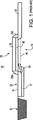
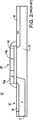
該基板上に形成されたゲート誘電体層と、該ゲート誘電体層上に形成されたデュアル仕事関数ゲート導体層とを含むトランスファゲートデバイス、
該デュアル仕事関数ゲート導体層は、第1導電性タイプ材料から成る第1ドープ領域及び第2導電性タイプ材料から成る第2ドープ領域を含む;
入射する光に応答して電荷キャリヤを捕集するための、前記トランスファゲートデバイスの前記第1ドープ領域に隣接する基板表面に又は該基板表面の下側に形成されたフォトセンシングデバイス;
前記トランスファゲートデバイスの前記第2ドープ領域に隣接する前記基板表面に形成された、第2導電性タイプ材料から成る拡散領域、
該トランスファゲートデバイスは、前記フォトセンシングデバイスと前記拡散領域との間の電荷移動を可能にするチャネル領域を形成している;及び
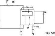
前記トランスファゲートデバイスの第1導電性タイプ材料から成る前記第1ドープ領域と、前記トランスファゲートデバイスの第2導電性タイプ材料から成る前記第2ドープ領域とを電気的にカップリングするための、前記デュアル仕事関数ゲート導体層の最上部に形成されたシリサイド構造
を含んで成る。
Claims (3)
- 第1導電性タイプ材料から成る基板;
該基板上に形成されたゲート誘電体層と、該ゲート誘電体層上に形成されたデュアル仕事関数ゲート導体層とを含むトランスファゲートデバイス、
該デュアル仕事関数ゲート導体層は、第1導電性タイプ材料から成る第1ドープ領域及び第2導電性タイプ材料から成る第2ドープ領域を含む;
入射する光に応答して電荷キャリヤを捕集するための、前記トランスファゲートデバイスの前記第1ドープ領域に隣接する基板表面に又は該基板表面の下側に形成されたフォトセンシングデバイス;
前記トランスファゲートデバイスの前記第2ドープ領域に隣接する前記基板表面に形成された、第2導電性タイプ材料から成る拡散領域、
該トランスファゲートデバイスは、前記フォトセンシングデバイスと前記拡散領域との間の電荷移動を可能にするチャネル領域を形成している;及び
前記トランスファゲートデバイスの第1導電性タイプ材料から成る前記第1ドープ領域と、前記トランスファゲートデバイスの第2導電性タイプ材料から成る前記第2ドープ領域とを電気的にカップリングするための、前記デュアル仕事関数ゲート導体層の最上部に形成されたシリサイド構造
を含んで成るアクティブピクセルセンサ(APS)セル構造であって、
前記シリサイド構造が、面積寸法で、前記デュアル仕事関数ゲート導体層の面積寸法よりも小さいアクティブピクセルセンサ(APS)セル構造。 - 前記APSセル構造が、アクティブピクセルセンサ(APS)セル構造をそれぞれ含んでいる各ピクセルを有するCMOS画像センサのピクセルアレイに含まれ、そして当該CMOS画像センサが、画像捕獲装置に含まれる、請求項1に記載のAPSセル構造。
- 第1導電性タイプ材料から成る基板を用意すること;
該基板上に形成されたゲート誘電体層及び該ゲート誘電体層上に形成されたデュアル仕事関数ゲート導体層を含むトランスファゲートデバイスを形成すること、
該デュアル仕事関数ゲート導体層は、第1導電性タイプ材料から成る第1ドープ領域及び第2導電性タイプ材料から成る第2ドープ領域を含む;
前記トランスファゲートデバイスの前記第1ドープ領域に隣接する基板表面に又は該基板表面の下側に形成された、入射する光に応答して電荷キャリヤを捕集するための、フォトセンシングデバイスを形成すること;
前記トランスファゲートデバイスの前記第2ドープ領域に隣接する前記基板表面ところに、第2導電性タイプ材料から成る拡散領域を形成すること、
前記トランスファゲートデバイスは、前記フォトセンシングデバイスと前記拡散領域との間の電荷移動を可能にするチャネル領域を形成する;そして
前記トランスファゲートデバイスの第1導電性タイプ材料から成る前記第1ドープ領域と、前記トランスファゲートデバイスの第2導電性タイプ材料から成る前記第2ドープ領域とを電気的にカップリングするための、前記デュアル仕事関数ゲート導体層の最上部にシリサイド構造を形成すること
を含んで成るアクティブピクセルセンサ(APS)セル構造を形成する方法であって、
前記シリサイド構造が、面積寸法で、前記デュアル仕事関数ゲート導体層の面積寸法よりも小さいアクティブピクセルセンサ(APS)セル構造を形成する方法。
Applications Claiming Priority (3)
| Application Number | Priority Date | Filing Date | Title |
|---|---|---|---|
| US11/565,801 | 2006-12-01 | ||
| US11/565,801 US7675097B2 (en) | 2006-12-01 | 2006-12-01 | Silicide strapping in imager transfer gate device |
| PCT/US2007/024684 WO2008069994A2 (en) | 2006-12-01 | 2007-11-30 | Silicide strapping in imager transfer gate device |
Publications (3)
| Publication Number | Publication Date |
|---|---|
| JP2010512004A JP2010512004A (ja) | 2010-04-15 |
| JP2010512004A5 JP2010512004A5 (ja) | 2011-01-20 |
| JP5096483B2 true JP5096483B2 (ja) | 2012-12-12 |
Family
ID=39434223
Family Applications (1)
| Application Number | Title | Priority Date | Filing Date |
|---|---|---|---|
| JP2009539352A Active JP5096483B2 (ja) | 2006-12-01 | 2007-11-30 | 撮像素子トランスファゲートデバイスにおけるシリサイドストラップ |
Country Status (7)
| Country | Link |
|---|---|
| US (2) | US7675097B2 (ja) |
| EP (1) | EP2089905B1 (ja) |
| JP (1) | JP5096483B2 (ja) |
| KR (1) | KR101437194B1 (ja) |
| CN (1) | CN101281918B (ja) |
| TW (1) | TWI420659B (ja) |
| WO (1) | WO2008069994A2 (ja) |
Families Citing this family (36)
| Publication number | Priority date | Publication date | Assignee | Title |
|---|---|---|---|---|
| US7838371B2 (en) * | 2006-11-06 | 2010-11-23 | Nxp B.V. | Method of manufacturing a FET gate |
| US7675097B2 (en) | 2006-12-01 | 2010-03-09 | International Business Machines Corporation | Silicide strapping in imager transfer gate device |
| KR100810423B1 (ko) * | 2006-12-27 | 2008-03-04 | 동부일렉트로닉스 주식회사 | 이미지 센서 및 이미지 센서의 제조 방법 |
| US20080217679A1 (en) * | 2007-03-08 | 2008-09-11 | Macronix International Co., Ltd. | Memory unit structure and operation method thereof |
| KR20090003854A (ko) * | 2007-07-05 | 2009-01-12 | 삼성전자주식회사 | 이미지 센서 및 그 제조 방법 |
| US8110465B2 (en) | 2007-07-30 | 2012-02-07 | International Business Machines Corporation | Field effect transistor having an asymmetric gate electrode |
| US7741217B2 (en) * | 2007-10-25 | 2010-06-22 | International Business Machines Corporation | Dual workfunction silicide diode |
| US8227844B2 (en) * | 2008-01-14 | 2012-07-24 | International Business Machines Corporation | Low lag transfer gate device |
| US8743247B2 (en) * | 2008-01-14 | 2014-06-03 | International Business Machines Corporation | Low lag transfer gate device |
| TWI347009B (en) * | 2008-02-04 | 2011-08-11 | Jack Kuo | Continuous multigate transistors |
| US20090261393A1 (en) * | 2008-04-18 | 2009-10-22 | United Microelectronics Corp. | Composite transfer gate and fabrication thereof |
| JP5271104B2 (ja) * | 2009-02-13 | 2013-08-21 | 浜松ホトニクス株式会社 | リニアイメージセンサ |
| JP5091886B2 (ja) | 2009-02-13 | 2012-12-05 | 浜松ホトニクス株式会社 | イメージセンサ |
| US20100314667A1 (en) * | 2009-06-11 | 2010-12-16 | Omnivision Technologies, Inc. | Cmos pixel with dual-element transfer gate |
| US9000500B2 (en) * | 2009-12-30 | 2015-04-07 | Omnivision Technologies, Inc. | Image sensor with doped transfer gate |
| US8299505B2 (en) | 2011-02-17 | 2012-10-30 | International Business Machines Corporation | Pixel sensor cell with a dual work function gate electode |
| US9123602B2 (en) | 2011-05-12 | 2015-09-01 | Olive Medical Corporation | Pixel array area optimization using stacking scheme for hybrid image sensor with minimal vertical interconnects |
| US9070784B2 (en) * | 2011-07-22 | 2015-06-30 | Taiwan Semiconductor Manufacturing Company, Ltd. | Metal gate structure of a CMOS semiconductor device and method of forming the same |
| JP2013084834A (ja) * | 2011-10-12 | 2013-05-09 | Sharp Corp | 固体撮像素子及び固体撮像素子の製造方法 |
| US9698185B2 (en) * | 2011-10-13 | 2017-07-04 | Omnivision Technologies, Inc. | Partial buried channel transfer device for image sensors |
| US9000527B2 (en) | 2012-05-15 | 2015-04-07 | Apple Inc. | Gate stack with electrical shunt in end portion of gate stack |
| WO2014002365A1 (ja) * | 2012-06-26 | 2014-01-03 | パナソニック株式会社 | 固体撮像装置及びその製造方法 |
| CN111938543A (zh) | 2012-07-26 | 2020-11-17 | 德普伊辛迪斯制品公司 | 具有最小面积单片式cmos图像传感器的相机系统 |
| US8809925B2 (en) * | 2012-10-11 | 2014-08-19 | Omnivision Technologies, Inc. | Partial buried channel transfer device in image sensors |
| US8912584B2 (en) * | 2012-10-23 | 2014-12-16 | Apple Inc. | PFET polysilicon layer with N-type end cap for electrical shunt |
| JP6433975B2 (ja) | 2013-03-15 | 2018-12-05 | デピュイ・シンセス・プロダクツ・インコーポレイテッド | 入力クロック及びデータ伝送クロックのない画像センサ同期 |
| BR112015022884A2 (pt) | 2013-03-15 | 2017-07-18 | Olive Medical Corp | minimizar o sensor de imagem i/o e as contagens do condutor em aplicações de endoscópio |
| KR102089682B1 (ko) * | 2013-07-15 | 2020-03-16 | 삼성전자 주식회사 | 반도체 장치 및 이의 제조 방법 |
| CN103456756A (zh) * | 2013-09-26 | 2013-12-18 | 哈尔滨工程大学 | 一种有源像素结构及其制作方法 |
| US9526468B2 (en) | 2014-09-09 | 2016-12-27 | General Electric Company | Multiple frame acquisition for exposure control in X-ray medical imagers |
| JP6668600B2 (ja) * | 2015-03-19 | 2020-03-18 | セイコーエプソン株式会社 | 固体撮像素子及びその製造方法 |
| TWI724164B (zh) * | 2017-05-05 | 2021-04-11 | 聯華電子股份有限公司 | 半導體元件及其製作方法 |
| US11393867B2 (en) * | 2017-12-06 | 2022-07-19 | Facebook Technologies, Llc | Multi-photodiode pixel cell |
| CN111868929B (zh) * | 2018-02-23 | 2021-08-03 | 奥特逻科公司 | 光检测装置及其光检测方法 |
| CN110108919A (zh) * | 2019-04-16 | 2019-08-09 | 天津大学 | 一种像素内PPD pinning电压的测量方法 |
| WO2022137864A1 (ja) * | 2020-12-21 | 2022-06-30 | ソニーセミコンダクタソリューションズ株式会社 | 撮像装置及び電子機器 |
Family Cites Families (21)
| Publication number | Priority date | Publication date | Assignee | Title |
|---|---|---|---|---|
| JP2817518B2 (ja) * | 1991-06-21 | 1998-10-30 | 松下電器産業株式会社 | 半導体装置およびその製造方法 |
| DE69630944D1 (de) | 1996-03-29 | 2004-01-15 | St Microelectronics Srl | Hochspannungsfester MOS-Transistor und Verfahren zur Herstellung |
| EP0936667A1 (en) * | 1998-01-20 | 1999-08-18 | Lucent Technologies Inc. | Lattice matched barrier for dual doped polysilicon gates |
| US6333205B1 (en) * | 1999-08-16 | 2001-12-25 | Micron Technology, Inc. | CMOS imager with selectively silicided gates |
| JP4398917B2 (ja) | 2000-03-28 | 2010-01-13 | 株式会社東芝 | 固体撮像装置及びその製造方法 |
| JP3782297B2 (ja) * | 2000-03-28 | 2006-06-07 | 株式会社東芝 | 固体撮像装置及びその製造方法 |
| JP2004506388A (ja) * | 2000-08-04 | 2004-02-26 | フォベオン・インコーポレーテッド | 完全電子化高解像度ディジタルスチルカメラ |
| US6794252B2 (en) * | 2001-09-28 | 2004-09-21 | Texas Instruments Incorporated | Method and system for forming dual work function gate electrodes in a semiconductor device |
| TWI296062B (en) * | 2001-12-28 | 2008-04-21 | Sanyo Electric Co | Liquid crystal display device |
| US7335958B2 (en) * | 2003-06-25 | 2008-02-26 | Micron Technology, Inc. | Tailoring gate work-function in image sensors |
| US7064406B2 (en) * | 2003-09-03 | 2006-06-20 | Micron Technology, Inc. | Supression of dark current in a photosensor for imaging |
| US7205584B2 (en) * | 2003-12-22 | 2007-04-17 | Micron Technology, Inc. | Image sensor for reduced dark current |
| US7214575B2 (en) * | 2004-01-06 | 2007-05-08 | Micron Technology, Inc. | Method and apparatus providing CMOS imager device pixel with transistor having lower threshold voltage than other imager device transistors |
| JP2005260077A (ja) * | 2004-03-12 | 2005-09-22 | Matsushita Electric Ind Co Ltd | 固体撮像素子ならびにその製造方法およびそれを用いたカメラ |
| JP4546201B2 (ja) * | 2004-03-17 | 2010-09-15 | ルネサスエレクトロニクス株式会社 | 半導体装置の製造方法 |
| US7288788B2 (en) * | 2004-12-03 | 2007-10-30 | International Business Machines Corporation | Predoped transfer gate for an image sensor |
| US7217968B2 (en) | 2004-12-15 | 2007-05-15 | International Business Machines Corporation | Recessed gate for an image sensor |
| JP4533155B2 (ja) * | 2005-01-12 | 2010-09-01 | 富士通セミコンダクター株式会社 | 半導体装置及びその製造方法 |
| US7115924B1 (en) * | 2005-06-03 | 2006-10-03 | Avago Technologies Sensor Ip Pte. Ltd. | Pixel with asymmetric transfer gate channel doping |
| JP4847828B2 (ja) * | 2006-09-22 | 2011-12-28 | 旭化成エレクトロニクス株式会社 | Cmosイメージセンサの製造方法 |
| US7675097B2 (en) | 2006-12-01 | 2010-03-09 | International Business Machines Corporation | Silicide strapping in imager transfer gate device |
-
2006
- 2006-12-01 US US11/565,801 patent/US7675097B2/en active Active
-
2007
- 2007-11-15 CN CN2007101869334A patent/CN101281918B/zh active Active
- 2007-11-30 TW TW096145709A patent/TWI420659B/zh active
- 2007-11-30 KR KR1020097011278A patent/KR101437194B1/ko active IP Right Grant
- 2007-11-30 EP EP07867600.4A patent/EP2089905B1/en active Active
- 2007-11-30 JP JP2009539352A patent/JP5096483B2/ja active Active
- 2007-11-30 WO PCT/US2007/024684 patent/WO2008069994A2/en active Application Filing
-
2010
- 2010-02-03 US US12/699,419 patent/US8158453B2/en active Active
Also Published As
| Publication number | Publication date |
|---|---|
| US20100136733A1 (en) | 2010-06-03 |
| JP2010512004A (ja) | 2010-04-15 |
| CN101281918A (zh) | 2008-10-08 |
| EP2089905B1 (en) | 2014-01-22 |
| WO2008069994A3 (en) | 2008-08-28 |
| KR101437194B1 (ko) | 2014-09-03 |
| US7675097B2 (en) | 2010-03-09 |
| WO2008069994A2 (en) | 2008-06-12 |
| EP2089905A2 (en) | 2009-08-19 |
| TW200837941A (en) | 2008-09-16 |
| KR20090087896A (ko) | 2009-08-18 |
| CN101281918B (zh) | 2010-12-08 |
| US8158453B2 (en) | 2012-04-17 |
| US20080128767A1 (en) | 2008-06-05 |
| TWI420659B (zh) | 2013-12-21 |
Similar Documents
| Publication | Publication Date | Title |
|---|---|---|
| JP5096483B2 (ja) | 撮像素子トランスファゲートデバイスにおけるシリサイドストラップ | |
| US8227844B2 (en) | Low lag transfer gate device | |
| US7888156B2 (en) | Predoped transfer gate for a CMOS image sensor | |
| US8743247B2 (en) | Low lag transfer gate device | |
| US7217968B2 (en) | Recessed gate for an image sensor | |
| US7205591B2 (en) | Pixel sensor cell having reduced pinning layer barrier potential and method thereof | |
| US7141836B1 (en) | Pixel sensor having doped isolation structure sidewall | |
| US8268662B2 (en) | Fabricating method of complementary metal-oxide-semiconductor (CMOS) image sensor | |
| US7528427B2 (en) | Pixel sensor cell having asymmetric transfer gate with reduced pinning layer barrier potential | |
| US20060276014A1 (en) | Self-aligned high-energy implantation for deep junction structure | |
| US7768087B2 (en) | Photodiode, solid slate image sensor, and method of manufacturing the same | |
| US8004027B2 (en) | Image sensor and manufacturing method thereof | |
| US7429496B2 (en) | Buried photodiode for image sensor with shallow trench isolation technology | |
| US20070023796A1 (en) | Pinning layer for pixel sensor cell and method thereof | |
| US8679884B2 (en) | Methods for manufacturing semiconductor apparatus and CMOS image sensor | |
| KR20050029455A (ko) | 씨모스 이미지 센서 및 그 제조 방법 | |
| US20060284223A1 (en) | CMOS image sensor and manufacturing method thereof | |
| US7145190B2 (en) | Pinned photodiode integrated with trench isolation and fabrication method | |
| KR100790213B1 (ko) | 이미지센서의 제조 방법 |
Legal Events
| Date | Code | Title | Description |
|---|---|---|---|
| A521 | Request for written amendment filed |
Free format text: JAPANESE INTERMEDIATE CODE: A523 Effective date: 20101126 |
|
| A621 | Written request for application examination |
Free format text: JAPANESE INTERMEDIATE CODE: A621 Effective date: 20101126 |
|
| A711 | Notification of change in applicant |
Free format text: JAPANESE INTERMEDIATE CODE: A711 Effective date: 20111031 |
|
| A521 | Request for written amendment filed |
Free format text: JAPANESE INTERMEDIATE CODE: A821 Effective date: 20111031 |
|
| A521 | Request for written amendment filed |
Free format text: JAPANESE INTERMEDIATE CODE: A523 Effective date: 20111125 |
|
| TRDD | Decision of grant or rejection written | ||
| A01 | Written decision to grant a patent or to grant a registration (utility model) |
Free format text: JAPANESE INTERMEDIATE CODE: A01 Effective date: 20120821 |
|
| A01 | Written decision to grant a patent or to grant a registration (utility model) |
Free format text: JAPANESE INTERMEDIATE CODE: A01 |
|
| A977 | Report on retrieval |
Free format text: JAPANESE INTERMEDIATE CODE: A971007 Effective date: 20120823 |
|
| A61 | First payment of annual fees (during grant procedure) |
Free format text: JAPANESE INTERMEDIATE CODE: A61 Effective date: 20120920 |
|
| R150 | Certificate of patent or registration of utility model |
Ref document number: 5096483 Country of ref document: JP Free format text: JAPANESE INTERMEDIATE CODE: R150 Free format text: JAPANESE INTERMEDIATE CODE: R150 |
|
| FPAY | Renewal fee payment (event date is renewal date of database) |
Free format text: PAYMENT UNTIL: 20150928 Year of fee payment: 3 |
|
| R250 | Receipt of annual fees |
Free format text: JAPANESE INTERMEDIATE CODE: R250 |
|
| R250 | Receipt of annual fees |
Free format text: JAPANESE INTERMEDIATE CODE: R250 |
|
| R250 | Receipt of annual fees |
Free format text: JAPANESE INTERMEDIATE CODE: R250 |
|
| R250 | Receipt of annual fees |
Free format text: JAPANESE INTERMEDIATE CODE: R250 |
|
| R250 | Receipt of annual fees |
Free format text: JAPANESE INTERMEDIATE CODE: R250 |
|
| R250 | Receipt of annual fees |
Free format text: JAPANESE INTERMEDIATE CODE: R250 |
|
| R250 | Receipt of annual fees |
Free format text: JAPANESE INTERMEDIATE CODE: R250 |
|
| R250 | Receipt of annual fees |
Free format text: JAPANESE INTERMEDIATE CODE: R250 |
|
| R250 | Receipt of annual fees |
Free format text: JAPANESE INTERMEDIATE CODE: R250 |