EP2086291A2 - Beleuchtungsgerät mit Entladungsschaltung - Google Patents
Beleuchtungsgerät mit Entladungsschaltung Download PDFInfo
- Publication number
- EP2086291A2 EP2086291A2 EP09001543A EP09001543A EP2086291A2 EP 2086291 A2 EP2086291 A2 EP 2086291A2 EP 09001543 A EP09001543 A EP 09001543A EP 09001543 A EP09001543 A EP 09001543A EP 2086291 A2 EP2086291 A2 EP 2086291A2
- Authority
- EP
- European Patent Office
- Prior art keywords
- discharge lamp
- cycle
- period
- circuit
- power source
- Prior art date
- Legal status (The legal status is an assumption and is not a legal conclusion. Google has not performed a legal analysis and makes no representation as to the accuracy of the status listed.)
- Granted
Links
- 230000003247 decreasing effect Effects 0.000 claims description 11
- 238000004804 winding Methods 0.000 description 16
- 238000001514 detection method Methods 0.000 description 9
- 230000009467 reduction Effects 0.000 description 4
- 238000009499 grossing Methods 0.000 description 3
- 238000010586 diagram Methods 0.000 description 2
- 238000010438 heat treatment Methods 0.000 description 2
- 238000004519 manufacturing process Methods 0.000 description 2
- 230000009471 action Effects 0.000 description 1
- 230000008859 change Effects 0.000 description 1
- 230000005669 field effect Effects 0.000 description 1
- 238000000034 method Methods 0.000 description 1
- 230000003287 optical effect Effects 0.000 description 1
- 230000001360 synchronised effect Effects 0.000 description 1
- 230000007704 transition Effects 0.000 description 1
- 230000001960 triggered effect Effects 0.000 description 1
Images


Classifications
-
- H—ELECTRICITY
- H05—ELECTRIC TECHNIQUES NOT OTHERWISE PROVIDED FOR
- H05B—ELECTRIC HEATING; ELECTRIC LIGHT SOURCES NOT OTHERWISE PROVIDED FOR; CIRCUIT ARRANGEMENTS FOR ELECTRIC LIGHT SOURCES, IN GENERAL
- H05B41/00—Circuit arrangements or apparatus for igniting or operating discharge lamps
- H05B41/14—Circuit arrangements
- H05B41/26—Circuit arrangements in which the lamp is fed by power derived from DC by means of a converter, e.g. by high-voltage DC
- H05B41/28—Circuit arrangements in which the lamp is fed by power derived from DC by means of a converter, e.g. by high-voltage DC using static converters
- H05B41/288—Circuit arrangements in which the lamp is fed by power derived from DC by means of a converter, e.g. by high-voltage DC using static converters with semiconductor devices and specially adapted for lamps without preheating electrodes, e.g. for high-intensity discharge lamps, high-pressure mercury or sodium lamps or low-pressure sodium lamps
- H05B41/2885—Static converters especially adapted therefor; Control thereof
- H05B41/2887—Static converters especially adapted therefor; Control thereof characterised by a controllable bridge in the final stage
Definitions
- the present disclosure relates to a discharge lamp lighting circuit for preventing a discharge lamp from going out unexpectedly.
- the lighting frequency is decreased in one cycle right after the start of the discharge lamp.
- This one cycle will be referred to as a DC period.
- the electron emitting property for emitting electrons from the electrode is relatively poor right after the polarity is changed. Therefore, the electron emitting property is enhanced by increasing the duration of heating the electrode when the frequency is decreased below the frequency at the time of steady lighting. In this way, the change-over of the polarity at the first time can be accomplished easily.
- the DC period is too long, the life of the discharge lamp is affected.
- an upper limit of the product of the electric current in the DC period and the time is determined as the rating.
- This product of the electric current and the time will be referred to as the IT product.
- Concerning the cycle of the DC period two systems are provided. In one system, the cycle of the DC period is always set constant regardless of the power source voltage, the state of the discharge lamp and the atmospheric temperature. In the other system, the cycle of the DC period is determined while the electric current and the time are being operated so that the IT product can become constant.
- Japanese Patent Document JP-A-2002-216982 discloses a discharge lamp lighting circuit by which the DC period is determined when the IT product has reached a predetermined threshold value.
- the DC period is determined by the rated electric power supplied to the discharge lamp. Therefore, in the case where the electric power supplied to the discharge lamp is reduced below the rated electric power because the power source voltage of the discharge lamp lighting circuit is decreased or the temperature of the discharge lamp lighting circuit is high, the electrode is not sufficiently heated in the DC period. Accordingly, there is a possibility that the discharge lamp goes out unexpectedly at the time of the first change-over of the polarity.
- the present disclosure describes a discharge lamp lighting circuit that can help prevent a discharge lamp from going out unexpectedly.
- a DC period can be generated by a relatively small circuit according to the state of the discharge lamp and also according to a state of the discharge lamp lighting circuit.
- a discharge lamp lighting circuit for lighting a discharge lamp comprises: a boosting AC converter which receives a power source voltage, and boosts and converts the power source voltage into AC and supplies AC power to the discharge lamp.
- a control circuit is arranged to send a long cycle signal, the cycle of which is longer than a frequency at the time of steady lighting, when the discharge lamp is started, and to send a steady drive signal, which is a frequency at the time of steady lighting, to the boosting AC converter.
- the cycle of the long cycle signal is set by at least one of the power source voltage, the temperature of the discharge lamp lighting circuit, or the extinguishing time.
- the extinguishing time is a time from when the lighting state is finished till when the lighting operation is performed again in the case of restarting a discharge lamp (hot restart) by the discharge lamp lighting circuit.
- the cycle of the long cycle signal is set so that the discharge lamp can be prevented from going out unexpectedly.
- control circuit sets the cycle of the long cycle signal to be longer as the power source voltage is decreased.
- the control circuit sets the cycle of the long cycle signal to be longer as the extinguishing time is increased.
- the control circuit sets the cycle of the long cycle signal to be longer as the temperature of the discharge lamp lighting circuit is raised.
- the control circuit sets the cycle of the long cycle signal to be dispersed.
- a discharge lamp lighting circuit capable of preventing the discharge lamp from going out unexpectedly when the DC period corresponding to a state of the discharge lamp and also corresponding to a state of the discharge lamp lighting circuit is generated by a relatively small circuit of an open loop.
- the electric discharge lamp lighting circuit described below can be used, for example, for a headlight of a lighting device of an automobile.
- the cycle of the DC period in which a lighting frequency of only one cycle right after the start of the discharge lamp is decreased, is changed according to at least one of the electric power supplied to the discharge lamp, the power source voltage, the temperature of the discharge lamp lighting circuit or the extinguishing time of the discharge lamp.
- the cycle of the DC period is determined.
- the discharge lamp lighting circuit includes: a DC power source 1 such as a battery; a DC-DC converter 23; a DC-AC inverter 25; a starting circuit 24; and a control portion 22 for controlling the discharge lamp 21 so that it can be turned on and off.
- the DC-DC converter 23 receives an input voltage from the DC power source 1 and converts it to a predetermined DC voltage.
- a fly-back type DC-DC converter is employed. That is, the DC input voltage, which is supplied through the lighting switch 2 connected to the positive electrode side of the DC power source 1, is supplied to the primary side of the transformer 6 through the inductor 4.
- the switching element 8 connected to the primary side winding 6a of the transformer 6 and the rectifying and smoothing circuit 26 provided on the secondary side winding 6b of the transformer 6 can be used for the DC-DC converter 23.
- Fig. 1 when the windings 6a, 6b of the transformer 6 are attached with black circles, the starting points of the windings 6a, 6b are clearly indicated. That is, the polarity of each winding is shown.
- the inductor 4 and the condenser 5 are connected to the winding start end side terminal of the primary side winding 6a of the transformer 6..
- One end of the secondary side winding 6b (the winding start end side terminal) is connected to the winding end side terminal of the primary side winding 6a..
- the switching element 8 is connected to the winding end side terminal of the primary side winding 6a..
- a signal is sent from the control circuit 22 to the switching element 8..
- an N-channel MOS type FET the field effect transistor
- a drain of the FET is connected to one end of the winding 6a, 6b, and the source is grounded.
- the switching element is turned on and off.
- One end of the condenser 3 is connected to a terminal on the lighting switch 2 side of the inductor 4. The other end is connected to the negative electrode side of the DC power source 1.
- the rectifying diode 7 and the smoothing condenser 9, which form the rectifying and smoothing circuit 26, are provided on the secondary side of the transformer 6. That is, the winding end side terminal of the secondary side winding 6b of the transformer 6 is connected to the anode of the rectifying diode 7.
- the cathode of the diode 7 concerned is connected to one end of the condenser 9. The other end of the condenser 9 is grounded.
- the DC-AC inverter 25 includes: bridge drivers 15, 20, and switching elements 16 to 19.
- the DC-AC inverter 25 is provided for supplying electric power to the discharge lamp 21 through the starting circuit 24 after an output voltage of the DC-DC converted 23 has been converted into an AC voltage.
- the starting circuit 24 includes: a thyrister 10, a diode 14, a transformer 11, a condenser 12 and a resistor 13.
- the starting circuit 24 generates a high voltage pulse signal (a starting pulse) for starting the discharge lamp 21.
- the signal concerned is superimposed on the AC voltage from the DC-AC inverter 25 and applied to the discharge lamp 21.
- the control circuit 22 controls electric power provided to the discharge lamp 21 when the control circuit 22 receives the voltage given to the discharge lamp 21 and also receives the electric current flowing in the discharge lamp 21, or alternatively when the control circuit 22 receives detection signals corresponding to the voltage and the electric current. At the same time, the control circuit 22 controls an output of the DC-DC converter 23.
- control circuit 22 operates as follows.
- the control circuit 22 receives detection signals related to the output voltage and the electric current of the DC-DC converter 23.
- the control circuit 22 sends a control signal to the switching element 8 of the DC-DC converted 23 so as to control the output voltage.
- Concerning the switching control system, PWM system and PFM system are well known.
- the control circuit 22 sends a signal to the drive circuit 15, 20 of the DC-AC inverter 25 and controls operation of the bridge (e.g., a full bridge).
- a voltage supplied to the discharge lamp is raised to a predetermined level before the discharge lamp is turned on so that the discharge lamp can be positively turned on.
- the boosting AC converter is a combination of DC-DC converter 23 with the DC-AC inverter 25.
- the present invention is not limited to the above specific embodiment.
- the DC period is extended according to a reduction of the electric power provided to the discharge lamp. That is, in this discharge lamp lighting circuit, according to a decrease in the power source voltage and a rise of the temperature of the discharge lamp lighting circuit (overheat), electric power inputted into the discharge lamp is reduced so as to protect the discharge lamp lighting circuit. In the case where the discharge lamp is immediately started right after it has been turned off (in the case of restart), in order to suppress an optical output overshoot caused right after the discharge lamp is started, electric power provided to the discharge lamp is decreased corresponding to the extinguishing time of the discharge lamp. In this case, as described above, there is a possibility that the discharge lamp goes out unexpectedly due to the lack of heating the electrode of the discharge lamp.
- the cycle of the DC period is extended by reducing the power source voltage, as shown in Figs. 2 to 5 . That is, in the case where the cycle of the DC period is fixed, as shown in Fig. 2 , the cycle of the DC period becomes constant regardless of a change in the input voltage.
- the broken line shows the characteristic of the input electric power.
- the abscissa shows the power source voltage (V).
- the ordinate shows the electric power (W) provided to the discharge lamp.
- the solid line shows the characteristic of the cycle of the DC period.
- the horizontal axis shows the power source voltage (V) and the vertical axis shows the cycle (second) of the DC period.
- the cycle of the DC period is extended corresponding to a decrease in the power source voltage, as shown in Fig. 3 , the cycle of the DC period is extended as the input electric power is low, and the cycle of the DC period is shortened as the input electric power is high.
- the broken line shows the characteristic of the input electric power.
- the horizontal axis shows the power source voltage (V).
- the vertical axis shows the electric power (W) provided to the discharge lamp.
- the solid line shows the characteristic of the cycle of the DC period.
- the horizontal axis shows the power source voltage (V) and the vertical axis shows the cycle (second) of the DC period.
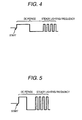
- a wave-form of the lamp current is shown in Figs. 4 and 5 .
- the cycle of the DC period is set long.
- the cycle of the DC period is set short.
- the electric power provided to the discharge lamp is determined when states of the discharge lamp lighting circuit and the power source voltage are monitored.
- the control portion circuit 22 of the discharge lamp lighting circuit judges a condition of reducing the electric power and operates an amount of the reduction of the electric power, an amount of the reduction of the electric power is already known.
- the DC period is prescribed by the IT product. Therefore, it is possible to determine the DC period from an amount of reduction of electric power. That is, even when the cycle of the DC period is not controlled while the IT product is being operated, it is possible to set an appropriate DC period. According to this method, the cycle of the DC period can be determined by open loop control. Therefore, it is possible to provide a discharge lamp lighting circuit, the starting property of which is excellent, using a relatively small circuit. Further, in the case of restarting a discharge lamp (hot restart), an amount of electric power is provided right after the start of the discharge lamp is reduced when the extinguishing time is short.
- an appropriate cycle of the DC period in which the life and the starting property are compatible with each other, is different from that in the case of a cold start.
- the cycle of the DC period is determined by the extinguishing time, it is possible to set an appropriate DC period in a hot restart.
- the power source voltage, the temperature of the discharge lamp lighting circuit and the extinguishing time are independent from each other. Therefore, when two or more parameters are combined with each other, an appropriate cycle of the DC period can be set.
- the extinguishing time is a time from when the lighting state is finished till when the lighting operation is performed again in the case of restarting a discharge lamp (hot restart) by the discharge lamp lighting circuit.
- Fig. 6 is a graph showing a relationship between the temperature of the discharge lamp lighting circuit and the input electric power and also showing a relationship between the temperature of the discharge lamp lighting circuit and the cycle of the DC period. As shown in Fig. 6 , as a temperature of the discharge lamp lighting circuit is raised, the cycle of the DC period is set longer.
- Fig. 7 is a graph showing a relationship between the temperature of the discharge lamp lighting circuit and the input electric power and also showing a relationship between the temperature of the discharge lamp lighting circuit and the cycle of the DC period and further showing a relationship between the temperature of the discharge lamp lighting circuit and the power source voltage. As shown in Fig. 7 , as the power source voltage is decreased, the cycle of the DC period is set to be long. Fig.
- FIG. 8 is a graph showing a relationship between the extinguishing time and the input electric power and also showing a relationship between the extinguishing time and the cycle of the DC period.
- the cycle of the DC period is set to be long.
- the broken line shows the characteristic of the input electric power
- the solid line shows the characteristic of the cycle of the DC period.
- the three broken lines or three solid lines are shown that as the power source voltage is decreased, the lines are shifted to the left.
- a resolution at which the cycle is continuously changed by analogous values, is not required. In many cases, it is sufficient that the cycle is changed by dispersed values. In many cases, the cycle of the DC period is generated by a digital circuit or software. Accordingly, when the cycle of the DC period is such that it can be changed by dispersed values, it is possible to reduce the circuit scale and the manufacturing cost.
- Fig. 9 shows an arrangement of the generating circuit for generating the cycle of the DC period.
- this generating circuit includes: a latch portion 50; a counter portion 51; and a comparison portion 52.
- This latch portion 50 has a function of latching (temporarily storing) the lighting information indicating whether or not the discharge lamp is turned on.
- the latch portion 50 is formed of a RS flip flop having two AND gates 101, 102. In the case where the discharge lamp is turned on, a signal of "L" is provided to the latch portion 50 as the lighting information described and temporarily stored.
- the counter portion 51 includes a synchronous counter having AND gates 103, 114 to 119, 121 to 124, JK flip flops 104 to 113 and OR gates 120, 125 to 127.
- Reset signals are provided to the reset terminals of these JK flip flop 104 to 113.
- One input of AND gate 103 is an output signal of the latch portion 50 and the other input is a clock signal of 5 kHz.
- the output signal of the AND gate 103 is provided to the clock terminal of the flip flops.
- the comparison portion 52 the output signals of JK flip flops 108 to 110 are provided to the terminals P0 to P2, and the output signals related to the set DC period are provided to the terminals Q0 to Q2. Both are compared with each other, and the result of the comparison is provided as an output.
- the cycle of the DC period is set by the circuit shown in Fig. 10 .
- the circuit shown in Fig. 10 includes: three operation amplifiers 200A to 200C; NOT gates 201A to 201C; AND gates 202, 203, 205; OR gates 204, 206; and NOT gate 207.
- the control parameter is provided to one input terminal (no inversion input) of each operation amplifier 200A to 200C..
- a value obtained when the reference voltage is divided by the resistors R1 to R4 is provided to the other input terminal (inversion input).
- “the control parameter” is a function of the power source voltage, the temperature of the discharge lamp lighting circuit or the extinguishing time.
- Output signals of the operation amplifiers 200A to 200C are supplied to the input terminals of AND gates 202, 203, 205 through NOT gates 201A to 201C.
- An output signal of AND gate 202 is supplied to one input terminal of OR gate 204.
- An output signal of AND gate 203 is supplied to the other input terminal of OR gate 204, 206.
- An output signal of AND gate 205 is supplied to the other input terminal of OR gate 206.
- An output signal of OR gate 204 is supplied to the terminal Q0 of the comparison portion 52.
- An output signal of OR gate 206 which passes through NOT gate 207, is supplied to the terminal Q1 of the comparison portion 52.
- An output signal of OR gate 206 is supplied to the terminal Q2 of the comparison portion 52.
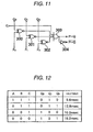
- the detailed arrangement of the comparison portion 52 is shown in Fig. 11 .
- the illustrated example of this comparison portion 52 includes: three ExNOR gates 300 to 302; AND gate 303; and NOT gate 304.
- the control parameter is entered in the circuit shown in Fig. 10 , and is set in the control circuit 22. Specifically, each control parameter is set by the circuit shown in Figs. 13 to 15 .
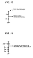
- the power source voltage detection circuit shown in Fig. 13 the power source voltage is divided by the resistors R10, R11. The divided voltage values are monitored so that a state of the power source voltage can be detected. The power source voltage information value becomes a low value when the power source voltage is low.
- diodes D1, D2, D3 are connected to the stabilized electric current source 400 in series. A voltage drop caused by the temperature characteristic of the diode is monitored, and the temperature information of the discharge lamp lighting circuit is provided as an output. The temperature information value is decreased when a temperature of the discharge lamp lighting circuit is high.
- An example of the extinguishing time detection circuit is shown in Fig. 15 .
- the switch 501 In the case where the switch 501 is turned on, an electric charge of the power source voltage 500 is accumulated in the condenser 503. In the case where the switch 501 is turned off, an electric charge of the power source voltage 500 is naturally discharged. Therefore, a charged voltage of the condenser 503 is detected, and the extinguishing time information is provided as an output.
- the extinguishing time information value is low when the extinguishing time is long.
- the present invention is not limited to the foregoing specific embodiment.
- FIG. 16 An arrangement of the circuit, by which a signal of level "L” is provided at the time of lighting the discharge lamp, is shown in Fig. 16 .
- the voltage of node “a” shown in Fig. 1 is provided to the inversion input terminal of the operation amplifier 600..
- the constant voltage 601 which is a threshold value of turning on and off, is provided to the no inversion input terminal..
- JK flip flop 111 already is maintained in the state of level "H". Therefore, a signal of level "H” is provided from AND gate 119 to J terminal of JK flip flop 112. As a result, from Q terminal of JK flip flop 112 concerned, a signal of level "H” is provided. As a result of the foregoing, JK flip flop 113 maintains a state of level "H". After that, the discharge lamp control is changed over to the lighting control executed by the steady lighting frequency.
- the binary number digital values of Q0 to Q2 are changed and the DC periods are dispersed in a range of9.6 msec to 19.2 msec (at a half wave) as shown in Fig. 12 .
- control parameters for setting the cycle of the DC period.
- other parameters may be used as control parameters.
Landscapes
- Circuit Arrangements For Discharge Lamps (AREA)
- Inverter Devices (AREA)
Applications Claiming Priority (1)
| Application Number | Priority Date | Filing Date | Title |
|---|---|---|---|
| JP2008024112A JP5112096B2 (ja) | 2008-02-04 | 2008-02-04 | 放電灯点灯回路 |
Publications (3)
| Publication Number | Publication Date |
|---|---|
| EP2086291A2 true EP2086291A2 (de) | 2009-08-05 |
| EP2086291A3 EP2086291A3 (de) | 2011-07-20 |
| EP2086291B1 EP2086291B1 (de) | 2012-12-05 |
Family
ID=40626802
Family Applications (1)
| Application Number | Title | Priority Date | Filing Date |
|---|---|---|---|
| EP09001543A Expired - Fee Related EP2086291B1 (de) | 2008-02-04 | 2009-02-04 | Beleuchtungsgerät mit Entladungsschaltung |
Country Status (3)
| Country | Link |
|---|---|
| US (1) | US8164270B2 (de) |
| EP (1) | EP2086291B1 (de) |
| JP (1) | JP5112096B2 (de) |
Families Citing this family (3)
| Publication number | Priority date | Publication date | Assignee | Title |
|---|---|---|---|---|
| TWI469416B (zh) * | 2012-04-03 | 2015-01-11 | 廣達電腦股份有限公司 | 充電電池模組、電池供電之電子裝置、以及電池充電方法 |
| JP5954659B2 (ja) | 2012-07-24 | 2016-07-20 | パナソニックIpマネジメント株式会社 | 点灯装置及びそれを用いた灯具並びに車両 |
| DE102014112823B4 (de) * | 2014-09-05 | 2016-07-21 | Infineon Technologies Ag | Halbleiterschalter mit integriertem Temperatursensor |
Citations (1)
| Publication number | Priority date | Publication date | Assignee | Title |
|---|---|---|---|---|
| JP2002216982A (ja) | 2001-01-12 | 2002-08-02 | Matsushita Electric Works Ltd | 放電灯点灯装置 |
Family Cites Families (11)
| Publication number | Priority date | Publication date | Assignee | Title |
|---|---|---|---|---|
| JPS6175621A (ja) * | 1984-09-21 | 1986-04-18 | Yokogawa Hokushin Electric Corp | 電圧一周波数変換器 |
| JPH07282986A (ja) * | 1994-04-15 | 1995-10-27 | Matsushita Electric Ind Co Ltd | 放電ランプ点灯装置 |
| JPH07335388A (ja) * | 1994-06-14 | 1995-12-22 | Matsushita Electric Ind Co Ltd | 放電ランプ点灯装置 |
| DE19509832A1 (de) * | 1995-03-17 | 1996-09-19 | Patent Treuhand Ges Fuer Elektrische Gluehlampen Mbh | Verfahren und Schaltungsanordnung zum Betrieb einer Entladungslampe |
| US6172468B1 (en) * | 1997-01-14 | 2001-01-09 | Metrolight Ltd. | Method and apparatus for igniting a gas discharge lamp |
| JP4208222B2 (ja) * | 1997-06-06 | 2009-01-14 | ハリソン東芝ライティング株式会社 | 前照灯用短アーク形メタルハライドランプ、メタルハライドランプ点灯装置および前照灯 |
| JPH11204285A (ja) * | 1998-01-07 | 1999-07-30 | Mitsubishi Electric Corp | 放電ランプ用点灯制御装置およびそれに用いる放電ランプ用ソケット |
| JP3807191B2 (ja) * | 2000-05-11 | 2006-08-09 | 松下電工株式会社 | 放電ランプ点灯装置 |
| JP4561097B2 (ja) * | 2003-12-26 | 2010-10-13 | パナソニック電工株式会社 | 放電灯点灯装置及び照明装置 |
| JP2008532251A (ja) * | 2005-03-04 | 2008-08-14 | インターナショナル レクティファイアー コーポレイション | 自動車用高輝度放電ランプ安定器回路 |
| JP5193445B2 (ja) * | 2006-08-23 | 2013-05-08 | パナソニック株式会社 | 高圧放電灯点灯装置及び照明器具 |
-
2008
- 2008-02-04 JP JP2008024112A patent/JP5112096B2/ja not_active Expired - Fee Related
-
2009
- 2009-02-02 US US12/363,853 patent/US8164270B2/en not_active Expired - Fee Related
- 2009-02-04 EP EP09001543A patent/EP2086291B1/de not_active Expired - Fee Related
Patent Citations (1)
| Publication number | Priority date | Publication date | Assignee | Title |
|---|---|---|---|---|
| JP2002216982A (ja) | 2001-01-12 | 2002-08-02 | Matsushita Electric Works Ltd | 放電灯点灯装置 |
Also Published As
| Publication number | Publication date |
|---|---|
| JP2009187708A (ja) | 2009-08-20 |
| JP5112096B2 (ja) | 2013-01-09 |
| US20090195176A1 (en) | 2009-08-06 |
| EP2086291B1 (de) | 2012-12-05 |
| US8164270B2 (en) | 2012-04-24 |
| EP2086291A3 (de) | 2011-07-20 |
Similar Documents
| Publication | Publication Date | Title |
|---|---|---|
| JP6904079B2 (ja) | スイッチング電源装置 | |
| JP6597239B2 (ja) | スイッチング電源装置 | |
| JP2010283616A (ja) | 照明光通信装置 | |
| JP4941036B2 (ja) | 放電管点灯装置及び半導体集積回路 | |
| EP1763289A1 (de) | Elektrisches Gerät für eine Entladungslampe | |
| JPH1197195A (ja) | 放電灯点灯回路 | |
| KR20060097534A (ko) | 스위칭 전원 회로의 제어 방식 | |
| JPH06215886A (ja) | 電源装置 | |
| CN101849438A (zh) | 高压放电灯点亮装置 | |
| EP2086291B1 (de) | Beleuchtungsgerät mit Entladungsschaltung | |
| JP2002354783A (ja) | 電源装置 | |
| JPH11168883A (ja) | Dc/dcコンバータ | |
| JP2001006890A (ja) | 放電灯点灯回路 | |
| JP2003276500A (ja) | 車両用照明灯装置 | |
| US7068020B2 (en) | Step-down DC—DC converter | |
| KR20130116206A (ko) | 방전등 점등 장치와, 그것을 구비한 차량탑재용 조명 장치 및 차량 | |
| JP2009272255A (ja) | 放電灯点灯装置、照明装置 | |
| JP2008289319A (ja) | 放電管電力供給装置及び半導体集積回路 | |
| JP3831983B2 (ja) | 放電灯点灯装置 | |
| JPH07118397B2 (ja) | 車輌用放電灯の点灯回路 | |
| JP4337791B2 (ja) | 放電灯点灯装置 | |
| JP4721937B2 (ja) | 放電灯点灯装置 | |
| JPS5911775A (ja) | スイツチングレギユレ−タ | |
| JPH09308255A (ja) | 放電灯点灯装置 | |
| JP4439667B2 (ja) | 非常用照明装置 |
Legal Events
| Date | Code | Title | Description |
|---|---|---|---|
| PUAI | Public reference made under article 153(3) epc to a published international application that has entered the european phase |
Free format text: ORIGINAL CODE: 0009012 |
|
| 17P | Request for examination filed |
Effective date: 20090204 |
|
| AK | Designated contracting states |
Kind code of ref document: A2 Designated state(s): AT BE BG CH CY CZ DE DK EE ES FI FR GB GR HR HU IE IS IT LI LT LU LV MC MK MT NL NO PL PT RO SE SI SK TR |
|
| AX | Request for extension of the european patent |
Extension state: AL BA RS |
|
| PUAL | Search report despatched |
Free format text: ORIGINAL CODE: 0009013 |
|
| AK | Designated contracting states |
Kind code of ref document: A3 Designated state(s): AT BE BG CH CY CZ DE DK EE ES FI FR GB GR HR HU IE IS IT LI LT LU LV MC MK MT NL NO PL PT RO SE SI SK TR |
|
| AX | Request for extension of the european patent |
Extension state: AL BA RS |
|
| AKX | Designation fees paid |
Designated state(s): DE FR GB |
|
| GRAP | Despatch of communication of intention to grant a patent |
Free format text: ORIGINAL CODE: EPIDOSNIGR1 |
|
| GRAS | Grant fee paid |
Free format text: ORIGINAL CODE: EPIDOSNIGR3 |
|
| GRAA | (expected) grant |
Free format text: ORIGINAL CODE: 0009210 |
|
| AK | Designated contracting states |
Kind code of ref document: B1 Designated state(s): DE FR GB |
|
| REG | Reference to a national code |
Ref country code: GB Ref legal event code: FG4D |
|
| REG | Reference to a national code |
Ref country code: DE Ref legal event code: R096 Ref document number: 602009011646 Country of ref document: DE Effective date: 20130131 |
|
| PGFP | Annual fee paid to national office [announced via postgrant information from national office to epo] |
Ref country code: GB Payment date: 20130130 Year of fee payment: 5 Ref country code: FR Payment date: 20130123 Year of fee payment: 5 Ref country code: DE Payment date: 20130226 Year of fee payment: 5 |
|
| PLBE | No opposition filed within time limit |
Free format text: ORIGINAL CODE: 0009261 |
|
| STAA | Information on the status of an ep patent application or granted ep patent |
Free format text: STATUS: NO OPPOSITION FILED WITHIN TIME LIMIT |
|
| 26N | No opposition filed |
Effective date: 20130906 |
|
| REG | Reference to a national code |
Ref country code: DE Ref legal event code: R097 Ref document number: 602009011646 Country of ref document: DE Effective date: 20130906 |
|
| REG | Reference to a national code |
Ref country code: DE Ref legal event code: R119 Ref document number: 602009011646 Country of ref document: DE |
|
| GBPC | Gb: european patent ceased through non-payment of renewal fee |
Effective date: 20140204 |
|
| REG | Reference to a national code |
Ref country code: FR Ref legal event code: ST Effective date: 20141031 |
|
| REG | Reference to a national code |
Ref country code: DE Ref legal event code: R119 Ref document number: 602009011646 Country of ref document: DE Effective date: 20140902 |
|
| PG25 | Lapsed in a contracting state [announced via postgrant information from national office to epo] |
Ref country code: DE Free format text: LAPSE BECAUSE OF NON-PAYMENT OF DUE FEES Effective date: 20140902 Ref country code: FR Free format text: LAPSE BECAUSE OF NON-PAYMENT OF DUE FEES Effective date: 20140228 Ref country code: GB Free format text: LAPSE BECAUSE OF NON-PAYMENT OF DUE FEES Effective date: 20140204 |