EP2062467B1 - Artikel mit beschichtung aus elektrisch leitendem polymer und edel-/halbedelmetal sowie herstellungsverfahren dafür - Google Patents
Artikel mit beschichtung aus elektrisch leitendem polymer und edel-/halbedelmetal sowie herstellungsverfahren dafür Download PDFInfo
- Publication number
- EP2062467B1 EP2062467B1 EP07801892A EP07801892A EP2062467B1 EP 2062467 B1 EP2062467 B1 EP 2062467B1 EP 07801892 A EP07801892 A EP 07801892A EP 07801892 A EP07801892 A EP 07801892A EP 2062467 B1 EP2062467 B1 EP 2062467B1
- Authority
- EP
- European Patent Office
- Prior art keywords
- layer
- copper
- iii
- coated article
- metal
- Prior art date
- Legal status (The legal status is an assumption and is not a legal conclusion. Google has not performed a legal analysis and makes no representation as to the accuracy of the status listed.)
- Not-in-force
Links
- 229910052751 metal Inorganic materials 0.000 title claims abstract description 61
- 239000002184 metal Substances 0.000 title claims abstract description 61
- 229920001940 conductive polymer Polymers 0.000 title claims abstract description 54
- 238000000034 method Methods 0.000 title claims abstract description 50
- 230000008569 process Effects 0.000 title claims abstract description 34
- 238000004519 manufacturing process Methods 0.000 title claims abstract description 15
- 238000000576 coating method Methods 0.000 title claims description 38
- 239000011248 coating agent Substances 0.000 title claims description 27
- 239000010949 copper Substances 0.000 claims abstract description 95
- 229910052802 copper Inorganic materials 0.000 claims abstract description 80
- RYGMFSIKBFXOCR-UHFFFAOYSA-N Copper Chemical compound [Cu] RYGMFSIKBFXOCR-UHFFFAOYSA-N 0.000 claims abstract description 73
- 239000000203 mixture Substances 0.000 claims abstract description 26
- 239000010970 precious metal Substances 0.000 claims abstract description 23
- 229910000881 Cu alloy Inorganic materials 0.000 claims abstract description 14
- 238000005260 corrosion Methods 0.000 claims abstract description 5
- 230000007797 corrosion Effects 0.000 claims abstract description 5
- 230000002265 prevention Effects 0.000 claims abstract description 4
- 239000006185 dispersion Substances 0.000 claims description 43
- 229910052709 silver Inorganic materials 0.000 claims description 36
- 239000010944 silver (metal) Substances 0.000 claims description 28
- 239000004332 silver Substances 0.000 claims description 26
- BQCADISMDOOEFD-UHFFFAOYSA-N Silver Chemical compound [Ag] BQCADISMDOOEFD-UHFFFAOYSA-N 0.000 claims description 25
- 229920000767 polyaniline Polymers 0.000 claims description 23
- 239000008139 complexing agent Substances 0.000 claims description 18
- 229910052737 gold Inorganic materials 0.000 claims description 17
- 239000010931 gold Substances 0.000 claims description 17
- -1 poly(3,4-ethylenedioxythiophene) Polymers 0.000 claims description 16
- 229920000123 polythiophene Polymers 0.000 claims description 14
- XSQUKJJJFZCRTK-UHFFFAOYSA-N Urea Chemical compound NC(N)=O XSQUKJJJFZCRTK-UHFFFAOYSA-N 0.000 claims description 13
- 229920000128 polypyrrole Polymers 0.000 claims description 13
- XLYOFNOQVPJJNP-UHFFFAOYSA-N water Substances O XLYOFNOQVPJJNP-UHFFFAOYSA-N 0.000 claims description 13
- BASFCYQUMIYNBI-UHFFFAOYSA-N platinum Substances [Pt] BASFCYQUMIYNBI-UHFFFAOYSA-N 0.000 claims description 11
- KDLHZDBZIXYQEI-UHFFFAOYSA-N palladium Substances [Pd] KDLHZDBZIXYQEI-UHFFFAOYSA-N 0.000 claims description 10
- UMGDCJDMYOKAJW-UHFFFAOYSA-N thiourea Chemical compound NC(N)=S UMGDCJDMYOKAJW-UHFFFAOYSA-N 0.000 claims description 10
- 229920001609 Poly(3,4-ethylenedioxythiophene) Polymers 0.000 claims description 9
- PCHJSUWPFVWCPO-UHFFFAOYSA-N gold Chemical compound [Au] PCHJSUWPFVWCPO-UHFFFAOYSA-N 0.000 claims description 9
- 229910052759 nickel Inorganic materials 0.000 claims description 9
- 239000002612 dispersion medium Substances 0.000 claims description 8
- 229910052763 palladium Inorganic materials 0.000 claims description 8
- 229910052697 platinum Inorganic materials 0.000 claims description 8
- 229910052719 titanium Inorganic materials 0.000 claims description 8
- 229910045601 alloy Inorganic materials 0.000 claims description 7
- 239000000956 alloy Substances 0.000 claims description 7
- 239000002322 conducting polymer Substances 0.000 claims description 7
- 150000001556 benzimidazoles Chemical class 0.000 claims description 6
- 150000001565 benzotriazoles Chemical class 0.000 claims description 6
- 229910052797 bismuth Inorganic materials 0.000 claims description 6
- 239000003795 chemical substances by application Substances 0.000 claims description 6
- 238000004140 cleaning Methods 0.000 claims description 6
- 239000002131 composite material Substances 0.000 claims description 6
- 150000002460 imidazoles Chemical class 0.000 claims description 6
- 229910052741 iridium Inorganic materials 0.000 claims description 6
- 229910052762 osmium Inorganic materials 0.000 claims description 6
- 229910052702 rhenium Inorganic materials 0.000 claims description 6
- 229910052703 rhodium Inorganic materials 0.000 claims description 6
- 239000010948 rhodium Substances 0.000 claims description 6
- 229910052707 ruthenium Inorganic materials 0.000 claims description 6
- 239000011135 tin Substances 0.000 claims description 6
- KCXVZYZYPLLWCC-UHFFFAOYSA-N EDTA Chemical compound OC(=O)CN(CC(O)=O)CCN(CC(O)=O)CC(O)=O KCXVZYZYPLLWCC-UHFFFAOYSA-N 0.000 claims description 5
- ATJFFYVFTNAWJD-UHFFFAOYSA-N Tin Chemical compound [Sn] ATJFFYVFTNAWJD-UHFFFAOYSA-N 0.000 claims description 5
- 229940071106 ethylenediaminetetraacetate Drugs 0.000 claims description 5
- NBGMRMDAEWWFIR-UHFFFAOYSA-N imidazole-2-thione Chemical class S=C1N=CC=N1 NBGMRMDAEWWFIR-UHFFFAOYSA-N 0.000 claims description 5
- 229910052718 tin Inorganic materials 0.000 claims description 5
- 239000004202 carbamide Substances 0.000 claims description 4
- 239000001913 cellulose Substances 0.000 claims description 4
- 229920002678 cellulose Polymers 0.000 claims description 4
- 150000002118 epoxides Chemical class 0.000 claims description 4
- 239000003960 organic solvent Substances 0.000 claims description 4
- 230000001590 oxidative effect Effects 0.000 claims description 4
- VKZRWSNIWNFCIQ-WDSKDSINSA-N (2s)-2-[2-[[(1s)-1,2-dicarboxyethyl]amino]ethylamino]butanedioic acid Chemical compound OC(=O)C[C@@H](C(O)=O)NCCN[C@H](C(O)=O)CC(O)=O VKZRWSNIWNFCIQ-WDSKDSINSA-N 0.000 claims description 3
- 238000001035 drying Methods 0.000 claims description 3
- 150000003892 tartrate salts Chemical class 0.000 claims description 3
- 239000004642 Polyimide Substances 0.000 claims description 2
- 239000004809 Teflon Substances 0.000 claims description 2
- 229920006362 Teflon® Polymers 0.000 claims description 2
- 239000000919 ceramic Substances 0.000 claims description 2
- 239000004643 cyanate ester Substances 0.000 claims description 2
- 239000007788 liquid Substances 0.000 claims description 2
- 229920001721 polyimide Polymers 0.000 claims description 2
- 238000002203 pretreatment Methods 0.000 claims description 2
- 239000004034 viscosity adjusting agent Substances 0.000 claims description 2
- JQDZNJOONPXQSL-UHFFFAOYSA-N [acetyloxy-[2-(diacetyloxyamino)ethyl]amino] acetate;sodium Chemical compound [Na].CC(=O)ON(OC(C)=O)CCN(OC(C)=O)OC(C)=O JQDZNJOONPXQSL-UHFFFAOYSA-N 0.000 claims 1
- 239000000306 component Substances 0.000 claims 1
- 239000010410 layer Substances 0.000 description 95
- SQGYOTSLMSWVJD-UHFFFAOYSA-N silver(1+) nitrate Chemical compound [Ag+].[O-]N(=O)=O SQGYOTSLMSWVJD-UHFFFAOYSA-N 0.000 description 24
- 238000005476 soldering Methods 0.000 description 20
- 238000012360 testing method Methods 0.000 description 20
- 238000005259 measurement Methods 0.000 description 18
- 230000032683 aging Effects 0.000 description 13
- 230000003647 oxidation Effects 0.000 description 11
- 238000007254 oxidation reaction Methods 0.000 description 11
- PAYRUJLWNCNPSJ-UHFFFAOYSA-N Aniline Chemical compound NC1=CC=CC=C1 PAYRUJLWNCNPSJ-UHFFFAOYSA-N 0.000 description 10
- 150000002739 metals Chemical class 0.000 description 10
- 239000000243 solution Substances 0.000 description 10
- 238000009736 wetting Methods 0.000 description 10
- 230000008859 change Effects 0.000 description 9
- 238000007654 immersion Methods 0.000 description 9
- 239000002105 nanoparticle Substances 0.000 description 9
- 239000000126 substance Substances 0.000 description 9
- 238000000151 deposition Methods 0.000 description 8
- 238000005530 etching Methods 0.000 description 8
- 239000000463 material Substances 0.000 description 8
- 239000000178 monomer Substances 0.000 description 8
- KAESVJOAVNADME-UHFFFAOYSA-N Pyrrole Chemical compound C=1C=CNC=1 KAESVJOAVNADME-UHFFFAOYSA-N 0.000 description 7
- 238000004833 X-ray photoelectron spectroscopy Methods 0.000 description 7
- YTPLMLYBLZKORZ-UHFFFAOYSA-N Thiophene Chemical compound C=1C=CSC=1 YTPLMLYBLZKORZ-UHFFFAOYSA-N 0.000 description 6
- KRKNYBCHXYNGOX-UHFFFAOYSA-N citric acid Chemical compound OC(=O)CC(O)(C(O)=O)CC(O)=O KRKNYBCHXYNGOX-UHFFFAOYSA-N 0.000 description 6
- 230000008021 deposition Effects 0.000 description 6
- 239000002245 particle Substances 0.000 description 6
- 239000000523 sample Substances 0.000 description 6
- MHAJPDPJQMAIIY-UHFFFAOYSA-N Hydrogen peroxide Chemical compound OO MHAJPDPJQMAIIY-UHFFFAOYSA-N 0.000 description 5
- 239000004020 conductor Substances 0.000 description 5
- 230000007423 decrease Effects 0.000 description 5
- 238000002845 discoloration Methods 0.000 description 5
- PXHVJJICTQNCMI-UHFFFAOYSA-N nickel Substances [Ni] PXHVJJICTQNCMI-UHFFFAOYSA-N 0.000 description 5
- 229920000642 polymer Polymers 0.000 description 5
- 230000009467 reduction Effects 0.000 description 5
- 238000001878 scanning electron micrograph Methods 0.000 description 5
- 229910000679 solder Inorganic materials 0.000 description 5
- 238000003869 coulometry Methods 0.000 description 4
- 230000000694 effects Effects 0.000 description 4
- 239000003792 electrolyte Substances 0.000 description 4
- 238000005516 engineering process Methods 0.000 description 4
- 150000002500 ions Chemical class 0.000 description 4
- 239000004922 lacquer Substances 0.000 description 4
- BDAGIHXWWSANSR-UHFFFAOYSA-N methanoic acid Natural products OC=O BDAGIHXWWSANSR-UHFFFAOYSA-N 0.000 description 4
- 239000000843 powder Substances 0.000 description 4
- 238000001228 spectrum Methods 0.000 description 4
- 238000003860 storage Methods 0.000 description 4
- 239000008399 tap water Substances 0.000 description 4
- 235000020679 tap water Nutrition 0.000 description 4
- JOXIMZWYDAKGHI-UHFFFAOYSA-N toluene-4-sulfonic acid Chemical compound CC1=CC=C(S(O)(=O)=O)C=C1 JOXIMZWYDAKGHI-UHFFFAOYSA-N 0.000 description 4
- ODPYDILFQYARBK-UHFFFAOYSA-N 7-thiabicyclo[4.1.0]hepta-1,3,5-triene Chemical compound C1=CC=C2SC2=C1 ODPYDILFQYARBK-UHFFFAOYSA-N 0.000 description 3
- QTBSBXVTEAMEQO-UHFFFAOYSA-N Acetic acid Chemical compound CC(O)=O QTBSBXVTEAMEQO-UHFFFAOYSA-N 0.000 description 3
- UHOVQNZJYSORNB-UHFFFAOYSA-N Benzene Chemical compound C1=CC=CC=C1 UHOVQNZJYSORNB-UHFFFAOYSA-N 0.000 description 3
- DGAQECJNVWCQMB-PUAWFVPOSA-M Ilexoside XXIX Chemical compound C[C@@H]1CC[C@@]2(CC[C@@]3(C(=CC[C@H]4[C@]3(CC[C@@H]5[C@@]4(CC[C@@H](C5(C)C)OS(=O)(=O)[O-])C)C)[C@@H]2[C@]1(C)O)C)C(=O)O[C@H]6[C@@H]([C@H]([C@@H]([C@H](O6)CO)O)O)O.[Na+] DGAQECJNVWCQMB-PUAWFVPOSA-M 0.000 description 3
- 239000002253 acid Substances 0.000 description 3
- 239000000654 additive Substances 0.000 description 3
- HSFWRNGVRCDJHI-UHFFFAOYSA-N alpha-acetylene Natural products C#C HSFWRNGVRCDJHI-UHFFFAOYSA-N 0.000 description 3
- 239000003125 aqueous solvent Substances 0.000 description 3
- 239000012298 atmosphere Substances 0.000 description 3
- 230000015572 biosynthetic process Effects 0.000 description 3
- 230000000052 comparative effect Effects 0.000 description 3
- PDZKZMQQDCHTNF-UHFFFAOYSA-M copper(1+);thiocyanate Chemical compound [Cu+].[S-]C#N PDZKZMQQDCHTNF-UHFFFAOYSA-M 0.000 description 3
- 238000013461 design Methods 0.000 description 3
- 239000002019 doping agent Substances 0.000 description 3
- 239000002421 finishing Substances 0.000 description 3
- 238000011835 investigation Methods 0.000 description 3
- 238000004626 scanning electron microscopy Methods 0.000 description 3
- 229910052708 sodium Inorganic materials 0.000 description 3
- 239000011734 sodium Substances 0.000 description 3
- 229930192474 thiophene Natural products 0.000 description 3
- 239000010936 titanium Substances 0.000 description 3
- YMMGRPLNZPTZBS-UHFFFAOYSA-N 2,3-dihydrothieno[2,3-b][1,4]dioxine Chemical compound O1CCOC2=C1C=CS2 YMMGRPLNZPTZBS-UHFFFAOYSA-N 0.000 description 2
- OSWFIVFLDKOXQC-UHFFFAOYSA-N 4-(3-methoxyphenyl)aniline Chemical compound COC1=CC=CC(C=2C=CC(N)=CC=2)=C1 OSWFIVFLDKOXQC-UHFFFAOYSA-N 0.000 description 2
- YLQBMQCUIZJEEH-UHFFFAOYSA-N Furan Chemical compound C=1C=COC=1 YLQBMQCUIZJEEH-UHFFFAOYSA-N 0.000 description 2
- XEEYBQQBJWHFJM-UHFFFAOYSA-N Iron Chemical compound [Fe] XEEYBQQBJWHFJM-UHFFFAOYSA-N 0.000 description 2
- AFVFQIVMOAPDHO-UHFFFAOYSA-N Methanesulfonic acid Chemical compound CS(O)(=O)=O AFVFQIVMOAPDHO-UHFFFAOYSA-N 0.000 description 2
- UFWIBTONFRDIAS-UHFFFAOYSA-N Naphthalene Chemical compound C1=CC=CC2=CC=CC=C21 UFWIBTONFRDIAS-UHFFFAOYSA-N 0.000 description 2
- QAOWNCQODCNURD-UHFFFAOYSA-N Sulfuric acid Chemical compound OS(O)(=O)=O QAOWNCQODCNURD-UHFFFAOYSA-N 0.000 description 2
- 239000003929 acidic solution Substances 0.000 description 2
- 150000007513 acids Chemical class 0.000 description 2
- 230000003679 aging effect Effects 0.000 description 2
- 150000001298 alcohols Chemical class 0.000 description 2
- QRUDEWIWKLJBPS-UHFFFAOYSA-N benzotriazole Chemical compound C1=CC=C2N[N][N]C2=C1 QRUDEWIWKLJBPS-UHFFFAOYSA-N 0.000 description 2
- 239000012964 benzotriazole Substances 0.000 description 2
- 238000006243 chemical reaction Methods 0.000 description 2
- 238000002149 energy-dispersive X-ray emission spectroscopy Methods 0.000 description 2
- 239000003822 epoxy resin Substances 0.000 description 2
- 235000019253 formic acid Nutrition 0.000 description 2
- 239000011521 glass Substances 0.000 description 2
- 239000002052 molecular layer Substances 0.000 description 2
- 150000002978 peroxides Chemical class 0.000 description 2
- 229920000172 poly(styrenesulfonic acid) Polymers 0.000 description 2
- 229920001197 polyacetylene Polymers 0.000 description 2
- 229920000647 polyepoxide Polymers 0.000 description 2
- 238000006116 polymerization reaction Methods 0.000 description 2
- 229910052700 potassium Inorganic materials 0.000 description 2
- 230000005588 protonation Effects 0.000 description 2
- 239000000758 substrate Substances 0.000 description 2
- 239000001117 sulphuric acid Substances 0.000 description 2
- 235000011149 sulphuric acid Nutrition 0.000 description 2
- 238000003786 synthesis reaction Methods 0.000 description 2
- VJYJJHQEVLEOFL-UHFFFAOYSA-N thieno[3,2-b]thiophene Chemical compound S1C=CC2=C1C=CS2 VJYJJHQEVLEOFL-UHFFFAOYSA-N 0.000 description 2
- 230000002110 toxicologic effect Effects 0.000 description 2
- 231100000027 toxicology Toxicity 0.000 description 2
- 230000007704 transition Effects 0.000 description 2
- 125000001140 1,4-phenylene group Chemical group [H]C1=C([H])C([*:2])=C([H])C([H])=C1[*:1] 0.000 description 1
- OYPRJOBELJOOCE-UHFFFAOYSA-N Calcium Chemical compound [Ca] OYPRJOBELJOOCE-UHFFFAOYSA-N 0.000 description 1
- OAICVXFJPJFONN-UHFFFAOYSA-N Phosphorus Chemical compound [P] OAICVXFJPJFONN-UHFFFAOYSA-N 0.000 description 1
- 229920000265 Polyparaphenylene Polymers 0.000 description 1
- ZLMJMSJWJFRBEC-UHFFFAOYSA-N Potassium Chemical compound [K] ZLMJMSJWJFRBEC-UHFFFAOYSA-N 0.000 description 1
- 229910021607 Silver chloride Inorganic materials 0.000 description 1
- 229910000831 Steel Inorganic materials 0.000 description 1
- NINIDFKCEFEMDL-UHFFFAOYSA-N Sulfur Chemical class [S] NINIDFKCEFEMDL-UHFFFAOYSA-N 0.000 description 1
- UCKMPCXJQFINFW-UHFFFAOYSA-N Sulphide Chemical compound [S-2] UCKMPCXJQFINFW-UHFFFAOYSA-N 0.000 description 1
- 230000002378 acidificating effect Effects 0.000 description 1
- 230000004913 activation Effects 0.000 description 1
- 239000004480 active ingredient Substances 0.000 description 1
- 230000000996 additive effect Effects 0.000 description 1
- 230000002411 adverse Effects 0.000 description 1
- 125000003545 alkoxy group Chemical group 0.000 description 1
- 125000000217 alkyl group Chemical group 0.000 description 1
- JXLHNMVSKXFWAO-UHFFFAOYSA-N azane;7-fluoro-2,1,3-benzoxadiazole-4-sulfonic acid Chemical compound N.OS(=O)(=O)C1=CC=C(F)C2=NON=C12 JXLHNMVSKXFWAO-UHFFFAOYSA-N 0.000 description 1
- BEHLMOQXOSLGHN-UHFFFAOYSA-N benzenamine sulfate Chemical compound OS(=O)(=O)NC1=CC=CC=C1 BEHLMOQXOSLGHN-UHFFFAOYSA-N 0.000 description 1
- 238000009835 boiling Methods 0.000 description 1
- 239000000872 buffer Substances 0.000 description 1
- 150000004648 butanoic acid derivatives Chemical class 0.000 description 1
- 239000011575 calcium Substances 0.000 description 1
- 229910052791 calcium Inorganic materials 0.000 description 1
- 239000003990 capacitor Substances 0.000 description 1
- 230000001427 coherent effect Effects 0.000 description 1
- 230000000536 complexating effect Effects 0.000 description 1
- 150000001875 compounds Chemical class 0.000 description 1
- 239000000470 constituent Substances 0.000 description 1
- 229920001577 copolymer Polymers 0.000 description 1
- 239000013078 crystal Substances 0.000 description 1
- 150000001913 cyanates Chemical class 0.000 description 1
- 230000001419 dependent effect Effects 0.000 description 1
- 238000001514 detection method Methods 0.000 description 1
- 239000000539 dimer Substances 0.000 description 1
- 239000002270 dispersing agent Substances 0.000 description 1
- 239000004815 dispersion polymer Substances 0.000 description 1
- 238000002848 electrochemical method Methods 0.000 description 1
- 238000001941 electron spectroscopy Methods 0.000 description 1
- 125000002534 ethynyl group Chemical group [H]C#C* 0.000 description 1
- 238000011156 evaluation Methods 0.000 description 1
- 238000002474 experimental method Methods 0.000 description 1
- 238000009472 formulation Methods 0.000 description 1
- MSNOMDLPLDYDME-UHFFFAOYSA-N gold nickel Chemical compound [Ni].[Au] MSNOMDLPLDYDME-UHFFFAOYSA-N 0.000 description 1
- 125000005549 heteroarylene group Chemical group 0.000 description 1
- 230000001771 impaired effect Effects 0.000 description 1
- 229910052742 iron Inorganic materials 0.000 description 1
- 229910021645 metal ion Inorganic materials 0.000 description 1
- 239000007769 metal material Substances 0.000 description 1
- 238000001465 metallisation Methods 0.000 description 1
- 229940098779 methanesulfonic acid Drugs 0.000 description 1
- 238000002156 mixing Methods 0.000 description 1
- 230000007935 neutral effect Effects 0.000 description 1
- QJGQUHMNIGDVPM-UHFFFAOYSA-N nitrogen group Chemical group [N] QJGQUHMNIGDVPM-UHFFFAOYSA-N 0.000 description 1
- 150000007524 organic acids Chemical class 0.000 description 1
- 235000005985 organic acids Nutrition 0.000 description 1
- 150000002894 organic compounds Chemical class 0.000 description 1
- 239000012044 organic layer Substances 0.000 description 1
- 229920000620 organic polymer Polymers 0.000 description 1
- 239000008188 pellet Substances 0.000 description 1
- 230000000737 periodic effect Effects 0.000 description 1
- 125000001997 phenyl group Chemical group [H]C1=C([H])C([H])=C(*)C([H])=C1[H] 0.000 description 1
- OFNHPGDEEMZPFG-UHFFFAOYSA-N phosphanylidynenickel Chemical compound [P].[Ni] OFNHPGDEEMZPFG-UHFFFAOYSA-N 0.000 description 1
- 239000006069 physical mixture Substances 0.000 description 1
- 239000004033 plastic Substances 0.000 description 1
- 229920003023 plastic Polymers 0.000 description 1
- 229920000052 poly(p-xylylene) Polymers 0.000 description 1
- 229920000058 polyacrylate Polymers 0.000 description 1
- 229920000015 polydiacetylene Polymers 0.000 description 1
- 229920002959 polymer blend Polymers 0.000 description 1
- 229940005642 polystyrene sulfonic acid Drugs 0.000 description 1
- 229920002451 polyvinyl alcohol Polymers 0.000 description 1
- 235000019422 polyvinyl alcohol Nutrition 0.000 description 1
- 235000013855 polyvinylpyrrolidone Nutrition 0.000 description 1
- 230000008092 positive effect Effects 0.000 description 1
- 239000011591 potassium Substances 0.000 description 1
- ZNNZYHKDIALBAK-UHFFFAOYSA-M potassium thiocyanate Chemical compound [K+].[S-]C#N ZNNZYHKDIALBAK-UHFFFAOYSA-M 0.000 description 1
- 229940116357 potassium thiocyanate Drugs 0.000 description 1
- 238000002360 preparation method Methods 0.000 description 1
- 239000003755 preservative agent Substances 0.000 description 1
- 238000012545 processing Methods 0.000 description 1
- 230000002035 prolonged effect Effects 0.000 description 1
- 239000011253 protective coating Substances 0.000 description 1
- 239000012925 reference material Substances 0.000 description 1
- 150000003839 salts Chemical class 0.000 description 1
- 238000010517 secondary reaction Methods 0.000 description 1
- 230000035945 sensitivity Effects 0.000 description 1
- 238000000926 separation method Methods 0.000 description 1
- HKZLPVFGJNLROG-UHFFFAOYSA-M silver monochloride Chemical compound [Cl-].[Ag+] HKZLPVFGJNLROG-UHFFFAOYSA-M 0.000 description 1
- 238000004088 simulation Methods 0.000 description 1
- GGCZERPQGJTIQP-UHFFFAOYSA-N sodium;9,10-dioxoanthracene-2-sulfonic acid Chemical compound [Na+].C1=CC=C2C(=O)C3=CC(S(=O)(=O)O)=CC=C3C(=O)C2=C1 GGCZERPQGJTIQP-UHFFFAOYSA-N 0.000 description 1
- 239000002904 solvent Substances 0.000 description 1
- 239000010959 steel Substances 0.000 description 1
- 239000004094 surface-active agent Substances 0.000 description 1
- 238000003878 thermal aging Methods 0.000 description 1
- 231100000167 toxic agent Toxicity 0.000 description 1
- 230000002588 toxic effect Effects 0.000 description 1
- 238000012546 transfer Methods 0.000 description 1
- WFKWXMTUELFFGS-UHFFFAOYSA-N tungsten Chemical compound [W] WFKWXMTUELFFGS-UHFFFAOYSA-N 0.000 description 1
- 150000003672 ureas Chemical class 0.000 description 1
- 229920002554 vinyl polymer Polymers 0.000 description 1
Images


Classifications
-
- H—ELECTRICITY
- H05—ELECTRIC TECHNIQUES NOT OTHERWISE PROVIDED FOR
- H05K—PRINTED CIRCUITS; CASINGS OR CONSTRUCTIONAL DETAILS OF ELECTRIC APPARATUS; MANUFACTURE OF ASSEMBLAGES OF ELECTRICAL COMPONENTS
- H05K3/00—Apparatus or processes for manufacturing printed circuits
- H05K3/22—Secondary treatment of printed circuits
- H05K3/24—Reinforcing the conductive pattern
- H05K3/245—Reinforcing conductive patterns made by printing techniques or by other techniques for applying conductive pastes, inks or powders; Reinforcing other conductive patterns by such techniques
- H05K3/247—Finish coating of conductors by using conductive pastes, inks or powders
-
- H—ELECTRICITY
- H05—ELECTRIC TECHNIQUES NOT OTHERWISE PROVIDED FOR
- H05K—PRINTED CIRCUITS; CASINGS OR CONSTRUCTIONAL DETAILS OF ELECTRIC APPARATUS; MANUFACTURE OF ASSEMBLAGES OF ELECTRICAL COMPONENTS
- H05K3/00—Apparatus or processes for manufacturing printed circuits
- H05K3/10—Apparatus or processes for manufacturing printed circuits in which conductive material is applied to the insulating support in such a manner as to form the desired conductive pattern
- H05K3/18—Apparatus or processes for manufacturing printed circuits in which conductive material is applied to the insulating support in such a manner as to form the desired conductive pattern using precipitation techniques to apply the conductive material
-
- C—CHEMISTRY; METALLURGY
- C25—ELECTROLYTIC OR ELECTROPHORETIC PROCESSES; APPARATUS THEREFOR
- C25D—PROCESSES FOR THE ELECTROLYTIC OR ELECTROPHORETIC PRODUCTION OF COATINGS; ELECTROFORMING; APPARATUS THEREFOR
- C25D3/00—Electroplating: Baths therefor
- C25D3/02—Electroplating: Baths therefor from solutions
- C25D3/38—Electroplating: Baths therefor from solutions of copper
-
- H—ELECTRICITY
- H05—ELECTRIC TECHNIQUES NOT OTHERWISE PROVIDED FOR
- H05K—PRINTED CIRCUITS; CASINGS OR CONSTRUCTIONAL DETAILS OF ELECTRIC APPARATUS; MANUFACTURE OF ASSEMBLAGES OF ELECTRICAL COMPONENTS
- H05K3/00—Apparatus or processes for manufacturing printed circuits
- H05K3/22—Secondary treatment of printed circuits
- H05K3/28—Applying non-metallic protective coatings
- H05K3/282—Applying non-metallic protective coatings for inhibiting the corrosion of the circuit, e.g. for preserving the solderability
-
- H—ELECTRICITY
- H05—ELECTRIC TECHNIQUES NOT OTHERWISE PROVIDED FOR
- H05K—PRINTED CIRCUITS; CASINGS OR CONSTRUCTIONAL DETAILS OF ELECTRIC APPARATUS; MANUFACTURE OF ASSEMBLAGES OF ELECTRICAL COMPONENTS
- H05K2201/00—Indexing scheme relating to printed circuits covered by H05K1/00
- H05K2201/02—Fillers; Particles; Fibers; Reinforcement materials
- H05K2201/0203—Fillers and particles
- H05K2201/0242—Shape of an individual particle
- H05K2201/0257—Nanoparticles
-
- H—ELECTRICITY
- H05—ELECTRIC TECHNIQUES NOT OTHERWISE PROVIDED FOR
- H05K—PRINTED CIRCUITS; CASINGS OR CONSTRUCTIONAL DETAILS OF ELECTRIC APPARATUS; MANUFACTURE OF ASSEMBLAGES OF ELECTRICAL COMPONENTS
- H05K2201/00—Indexing scheme relating to printed circuits covered by H05K1/00
- H05K2201/03—Conductive materials
- H05K2201/032—Materials
- H05K2201/0329—Intrinsically conductive polymer [ICP]; Semiconductive polymer
-
- H—ELECTRICITY
- H05—ELECTRIC TECHNIQUES NOT OTHERWISE PROVIDED FOR
- H05K—PRINTED CIRCUITS; CASINGS OR CONSTRUCTIONAL DETAILS OF ELECTRIC APPARATUS; MANUFACTURE OF ASSEMBLAGES OF ELECTRICAL COMPONENTS
- H05K2203/00—Indexing scheme relating to apparatus or processes for manufacturing printed circuits covered by H05K3/00
- H05K2203/12—Using specific substances
- H05K2203/121—Metallo-organic compounds
-
- H—ELECTRICITY
- H05—ELECTRIC TECHNIQUES NOT OTHERWISE PROVIDED FOR
- H05K—PRINTED CIRCUITS; CASINGS OR CONSTRUCTIONAL DETAILS OF ELECTRIC APPARATUS; MANUFACTURE OF ASSEMBLAGES OF ELECTRICAL COMPONENTS
- H05K3/00—Apparatus or processes for manufacturing printed circuits
- H05K3/02—Apparatus or processes for manufacturing printed circuits in which the conductive material is applied to the surface of the insulating support and is thereafter removed from such areas of the surface which are not intended for current conducting or shielding
- H05K3/06—Apparatus or processes for manufacturing printed circuits in which the conductive material is applied to the surface of the insulating support and is thereafter removed from such areas of the surface which are not intended for current conducting or shielding the conductive material being removed chemically or electrolytically, e.g. by photo-etch process
-
- Y—GENERAL TAGGING OF NEW TECHNOLOGICAL DEVELOPMENTS; GENERAL TAGGING OF CROSS-SECTIONAL TECHNOLOGIES SPANNING OVER SEVERAL SECTIONS OF THE IPC; TECHNICAL SUBJECTS COVERED BY FORMER USPC CROSS-REFERENCE ART COLLECTIONS [XRACs] AND DIGESTS
- Y10—TECHNICAL SUBJECTS COVERED BY FORMER USPC
- Y10T—TECHNICAL SUBJECTS COVERED BY FORMER US CLASSIFICATION
- Y10T428/00—Stock material or miscellaneous articles
- Y10T428/12—All metal or with adjacent metals
- Y10T428/12014—All metal or with adjacent metals having metal particles
- Y10T428/12028—Composite; i.e., plural, adjacent, spatially distinct metal components [e.g., layers, etc.]
- Y10T428/12049—Nonmetal component
-
- Y—GENERAL TAGGING OF NEW TECHNOLOGICAL DEVELOPMENTS; GENERAL TAGGING OF CROSS-SECTIONAL TECHNOLOGIES SPANNING OVER SEVERAL SECTIONS OF THE IPC; TECHNICAL SUBJECTS COVERED BY FORMER USPC CROSS-REFERENCE ART COLLECTIONS [XRACs] AND DIGESTS
- Y10—TECHNICAL SUBJECTS COVERED BY FORMER USPC
- Y10T—TECHNICAL SUBJECTS COVERED BY FORMER US CLASSIFICATION
- Y10T428/00—Stock material or miscellaneous articles
- Y10T428/12—All metal or with adjacent metals
- Y10T428/12493—Composite; i.e., plural, adjacent, spatially distinct metal components [e.g., layers, joint, etc.]
- Y10T428/125—Deflectable by temperature change [e.g., thermostat element]
- Y10T428/12514—One component Cu-based
-
- Y—GENERAL TAGGING OF NEW TECHNOLOGICAL DEVELOPMENTS; GENERAL TAGGING OF CROSS-SECTIONAL TECHNOLOGIES SPANNING OVER SEVERAL SECTIONS OF THE IPC; TECHNICAL SUBJECTS COVERED BY FORMER USPC CROSS-REFERENCE ART COLLECTIONS [XRACs] AND DIGESTS
- Y10—TECHNICAL SUBJECTS COVERED BY FORMER USPC
- Y10T—TECHNICAL SUBJECTS COVERED BY FORMER US CLASSIFICATION
- Y10T428/00—Stock material or miscellaneous articles
- Y10T428/12—All metal or with adjacent metals
- Y10T428/12493—Composite; i.e., plural, adjacent, spatially distinct metal components [e.g., layers, joint, etc.]
- Y10T428/12535—Composite; i.e., plural, adjacent, spatially distinct metal components [e.g., layers, joint, etc.] with additional, spatially distinct nonmetal component
- Y10T428/12556—Organic component
- Y10T428/12569—Synthetic resin
-
- Y—GENERAL TAGGING OF NEW TECHNOLOGICAL DEVELOPMENTS; GENERAL TAGGING OF CROSS-SECTIONAL TECHNOLOGIES SPANNING OVER SEVERAL SECTIONS OF THE IPC; TECHNICAL SUBJECTS COVERED BY FORMER USPC CROSS-REFERENCE ART COLLECTIONS [XRACs] AND DIGESTS
- Y10—TECHNICAL SUBJECTS COVERED BY FORMER USPC
- Y10T—TECHNICAL SUBJECTS COVERED BY FORMER US CLASSIFICATION
- Y10T428/00—Stock material or miscellaneous articles
- Y10T428/12—All metal or with adjacent metals
- Y10T428/12493—Composite; i.e., plural, adjacent, spatially distinct metal components [e.g., layers, joint, etc.]
- Y10T428/12771—Transition metal-base component
- Y10T428/12861—Group VIII or IB metal-base component
Definitions
- the present invention relates to coated articles which contain a layer of copper or a copper alloy and a layer with a combination of intrinsically electrically conductive polymer and precious metal and/or semiprecious metal, and which are printed circuit boards.
- Copper is one of the most widely used metallic materials of our time. Although copper is a semiprecious metal, this material is readily oxidizable, which often has an adverse effect on its use properties. This manifests itself not only visually but also has in particular practical technical disadvantages. Particular problems arise in the coating of printed circuit boards, which are then assembled in soldering processes, copper wires which are used as electrical conductors, or copper pipes. Finely divided copper powders are practically impossible to produce and use without oxidation protection.
- Copper is normally not, like iron and steel, provided with protective coatings which in the case of lacquers often have to be applied in several layers. Instead, as protection against copper corrosion, substances which form complexes with copper, such as for example imidazoles, benzimidazoles, benzotriazoles, and imidazole-2-thione, are predominantly used.
- Metallic coatings are in general very suitable for printed circuit boards, however they also display a number of disadvantages. Coatings with gold are expensive not only on account of the high gold price, but in addition require special processes for the application of the gold layer. For example, gold cannot be chemically applied in so-called horizontal plants but only in vertical plants, which results in additional high process costs. A further technical risk is the so-called "black pad" phenomenom, which is a corrosion phenomenom. Furthermore, soldered joints with a nickel-gold surface are not totally reliable because of the formation of a nickel-phosphor or phosphor phase which weakens the soldered joint.
- silver-plated copper pads often tarnish e.g. due to sulphur compounds contained in the air.
- mechanical strength and electric reliability of soldered joints on silver-plated copper pads is often greatly impaired by so-called "microvoids" which appear at the boundary surface (interface).
- Tin is admittedly satisfactory from the technical and economic point of view in particular when it is applied with the aid of an organic metal, such as for example in the ORMECON CSN-process of Ormecon GmbH, Ammersbek, Germany.
- an organic metal such as for example in the ORMECON CSN-process of Ormecon GmbH, Ammersbek, Germany.
- its deposition as a rule requires several minutes (e.g. between 15 and 25 minutes), which renders correspondingly large-sized plants necessary in order to ensure a high throughput.
- OSPs Organic Solderability Preservatives
- One of the disadvantages is that the coating is not visually detectable due to its thin layer thickness (less than 100 nm), which makes an initial quality check difficult.
- its resistance to aging - although clearly improved compared with conventional OSPs - is still much less than that of metallic coatings.
- a process for the production of metallized materials is known in which the material to be metallized is first coated with an intrinsically conductive polymer, the intrinsically conductive polymer is then activated by reduction and finally the metal is applied in a non-electrochemical manner, wherein the coated material is brought into contact with a solution of ions of the metal.
- the process is particularly suitable for the deposition of tin onto copper but also for the metallization of plastic surfaces.
- the object of the invention is thus to provide an organic coating which has almost all of the properties of metallic coatings on copper, or provide a metallic coating which can be applied as quickly and easily as organic coatings, without losing too many properties in the process. Also, the coating of the invention should be capable of being prepared with very good reproducibility, and should not show the disadvantages associated with the prior art processes discussed above.
- a coating is applied to copper which contains one or more intrinsically conductive polymers or organic (nano-) metal(s) precious metal(s) and/or semiprecious metal(s).
- the object is achieved through a coated article, which is a printed circuit board comprising
- Layers according to the invention can be prepared using a number of methods which are in common use in the field of nanotechnology. Particularly preferred are methods wherein the (semi)precious metal is dissolved in a dispersion of an intrinsically conducting polymer or organic nanometal and wherein the metal is deposited from this dispersion/solution.
- the disclosure on the details of the present invention relates to both the first and second aspect of the invention.
- the solution according to the invention is surprising in as much as it was not to be expected in the light of the state of the art that a nanoscopic layer which contains a precious metal and/or semiprecious metal and an electrically conductive polymer could be produced and displays properties which combine the positive properties of the organic layers and those of the precious metals, despite the layers being thinner by more than one order of magnitude than conventional metallic end layers for preserving solderability.
- the thickness of layer (iii) according to the first aspect of the invention is preferably less than 1 ⁇ m, which contradicts the general expectation, according to which a larger effect would be achieved with thicker layers.
- the thickness of layer (iii) is preferably at least ca. 10 nm.
- Particularly preferred are layer thicknesses of less than 500 nm such as 200 to 400 nm or 200 to 350 nm, e.g. about 300 nm, e.g. less than 200 nm. These values relate to the complete thickness of the layer, i.e. metallic and organic components.
- a method suitable to determine the layer thickness is an electrochemical determination (galvanostatic coulometric measurement for example) and / or determination by UPS.
- the (average) thickness of layer (iii) according to the second aspect of the invention is 100 nm or less in total and less than 10 nm insofar as the metal constituent is concerned. It can be determined by using methods well known in the art, for example electrochemically or by means of EDX (Energy Dispersive X-Ray Analysis). Preferably, there are no other materials between the layers (i), (ii) and (iii).
- the layer does not necessarily need to be homogeneous, it can be a more or less homogeneously thin layer or can be composed of individual particles with a somewhat bigger diameter, and their average thickness meeting the above mentioned criteria.
- the layer contains at least 80% by weight of precious or semiprecious metal. However, it is not necessarily homogeneous, of uniform thickness or uniform density.
- the (semi)precious metal can also be deposited in the form of nanoscopic spheres of 50 to 150 nm diameter. Those spheres are distributed regularly (from a statistical point of view) on the copper surface. However, preferably they are deposited along edges or grain boundaries. Sometimes and in particular when the density of the nanoscopic spheres increases, they may form lengthy chains. In order to achieve good results, it may be sufficient that only about 10% of the surface are coated with the (semi)precious metal. The resulting effective thickness of the layer is therefore, in the average, only a few nanometers, typically about 5 nm. It can be measured by using XPS.
- layer (iii) contains at least one electrically conductive polymer and, optionally, organic copper complexing agents, in particular nitrogen containing or other organic compounds capabable of forming complexes with copper in organic or aqueous solvents.
- the copper complexing agent is selected from the group of nitrogen containing heterocyclic compounds or urea derivatives.
- Preferred examples are imidazoles, benzimidazoles, benzotriazoles, imidazole-2-thione, thiourea, urea, (sodium)ethylenediaminetetraacetate (EDTA), (K, Na-)tartrates, ethylenediamine disuccinic acid.
- the conductive polymer is preferably used in the form of an organic metal. Combinations of different substances from this substance class can be used. In the context of this invention, if not otherwise stated, polymers are understood to mean organic polymers.
- Electrically conductive polymers or conductive polymers which are also described as “intrinsically conductive polymers", are understood to means substances which are built up of small molecule compounds (monomers), are at least oligomeric by polymerization, and thus contain at least 3 monomer units which are linked by chemical bonding, display a conjugated n-electron system in the neutral (non-conductive) state and can be converted by oxidation, reduction or protonation (which is often described as “doping") into an ionic form which is conductive.
- the conductivity is at least 10 -7 S/cm and is normally less than 10 5 S/cm.
- doping agents for example iodine, peroxides, and Lewis are used in the case of doping by oxidation, or for example sodium, potassium, calcium in the case of doping by reduction.
- Protic acids such as para-toluene sulfonic acid or polystyrenesulfonic acids or the like may be used for doping by protonation.
- Conductive polymers can be chemically exceptionally diverse in composition.
- monomers for example acetylene, benzene, naphthalene, pyrrole, aniline, thiophene, phenylene sulphide, peri-naphthalene and others, and derivatives thereof, such as sulpho-aniline, ethylenedioxythiophene, thieno-thiophene and others, and alkyl or alkoxy derivatives thereof or derivatives with other side-groups, such as sulphonate, phenyl and other side-groups, have proved useful.
- Combinations of the aforesaid monomers can also be used as monomers.
- aniline and phenylene sulphide are linked, and these A-B dimers then used as monomers.
- pyrrole, thiophene or alkylthiophenes, ethylenedioxythiophene, thieno-thiophene, aniline, phenylene sulphide and others can be bound together into A-B structures and these then converted into oligomers or polymers.
- conductive polymers display a more or less strong rise in conductivity with increasing temperature, which identifies them as non-metallic conductors.
- Other conductive polymers display a metallic behaviour at least in a temperature range close to room temperature in that their conductivity decreases with increasing temperature.
- a further method of recognizing metallic behaviour consists in the plotting of the so-called “reduced activation energy" of the conductivity against the temperature at low temperatures (down to near 0 K).
- Conductors with a metallic contribution to the conductivity display a positive gradient of the curve at low temperature. Such substances are described as "organic metals".
- Preferred intrinsically conductive polymers are those mentioned above.
- the conductive polymers used in the present invention are polyaniline (PAni), polythiophene (PTh), polypyrrole (PPy), poly(3,4-ethylenedioxythiophene) (PEDT), polythieno-thiophene (PTT) and derivatives thereof and mixtures thereof. Most preferred is polyaniline.
- Layer (iii) contains at least one precious metal which is selected from the group Ag, Au, Pt, Pd, Rh, Ir, Ru, Os and Re, and/or a semiprecious metal which is selected from Ni, Ti, Cu and Bi.
- Layer (iii) furthermore contains one or more intrinsically electrically conductive polymers or organic (nano-) metals or mixtures thereof, optionally together with other substances such as non-electrically conductive components, and / or copper complexing agents.
- layer (iii) contains polymer blends, that is mixtures of conductive polymer / organic metal (or a combination of several) with electrically non-conductive polymers.
- Particularly suitable as non-conducive polymers are water-soluble or water-dispersible polymers, in particular polystyrene-sulphonic acid, polyacrylates, polyvinyl butyrates, polyvinyl-pyrrolidones, polyvinyl alcohols and mixtures thereof.
- Conductive and non-conductive polymers are preferably used in the ratio of 1 : 1. 5. to 1 : 20.
- Layer (iii) can also contain further compounds like copper complexing agents and other additives, in particular viscosity modifiers, flow aids, drying aids, gloss improvers, flatting agents and mixtures thereof, preferably in a concentration of 0.01 to 40 wt %, preferably 0.10 to 5 wt. % additive relative to the mass of layer (iii).
- the other copper complexing agents can be for example imidazoles, benzimidazoles, benzotriazoles, imidazole-2-thione, thiourea and urea and comparable materials.
- layer (iii) preferably contains 15 to 40% conductive polymer and other copper complexing agents , and 15 to 40% precious metal(s) or semiprecious metal(s), relative to the mass of layer (iii).
- layer (iii) preferably contains more than 80% precious metal or semiprecious metal, in particular more than 80% to e.g. 90% or 95%, based on the mass of layer (i).
- complexing agents are imidazoles, benzimidazoles or comparable complexing agents, such as benzotriazoles, urea, thiourea, imidazole-2-thione, (sodium)ethylenediamine tetraacetate (EDTA), (K-; Na-) tartrates, ethylenediamine-disuccinic acid, and mixtures thereof, which are characterized by a relatively good thermal stability.
- base layer (i) all materials used in printed circuit board technology are-suitable, in particular epoxides and epoxide composites, Teflon, cyanate esters, ceramics, cellulose and cellulose composites, such as for example cardboard, materials based on these substances and flexible base layers, for example based on polyimide.
- the base layer preferably has a layer thickness of 0.1 to 3 mm.
- the copper layer or copper alloy layer (ii) preferably has a thickness of 5 to 210 ⁇ m, in particular 15 to 35 ⁇ m.
- a further metal or alloy layer (iv) can be positioned between layer (ii) and layer (iii).
- Layer (iv) preferably contains silver, tin, gold, palladium or platinum.
- layer (iv) mainly contains, i.e. more than 50 wt. % relative to the mass of layer (iv), one or several of the said metals.
- the said metals can in particular be present as an alloy with copper.
- layer (iv) consists exclusively of the said metals, either in pure form or in the form of an alloy.
- Layer (iv) preferably has a layer thickness of 10 to 800 nm.
- layer (iv) can contain organic components, in a concentration of preferably 1 to 80 wt. % relative to the total mass of layer (iv) (metal content 20 to 99 wt. %).
- Preferred organic components are conductive polymers or organic metals, or organic copper complexing agents such as thiourea or benzotriazoles.
- the articles according to the invention are printed circuit boards which are also described as boards. These are thin plates used for the assembly of electrical components, with holes through which the leads of components are inserted for further soldering.
- the disclosure relates to articles comprising a coating as defined with regard to both the first and second aspect of the invention as defined hereinabove.
- the copper or copper alloy layer (ii) is degreased and cleaned following step (1).
- the articles are preferably treated with normal commercial acidic cleaners. Cleaners based on sulphuric acid and citric acid, such as for example the cleaner ACL 7001 from Ormecon GmbH, are preferred.
- the articles are preferably left in the cleaning bath for about 2 minutes at 45°C and then washed with water.
- etching the copper or copper alloy layer (ii) oxidatively following step (1) or after the cleaning, for example by etching the surface with H 2 O 2 or inorganic peroxides.
- Suitable etching solutions are commercially available, for examples the hydrogen peroxide-containing solution Etch 7000 from Ormecon GmbH or other peroxides.
- the articles are preferably left in the etching solution for about 2 minutes at 30°C.
- the layer produced in step (1) is preferably structured by lithographic or etching processes, whereby the conductor track structure is created.
- layer (iii) is applied to the article by treating this, after rinsing with water, with a dispersion of the conductive polymer(s) or organic metal(s) in a dispersion agent which is liquid at room temperature, for example by immersion of the article in the dispersion or by application thereof onto the article.
- the electrically conductive polymer or polymers are preferably contained in the dispersion medium in colloidal form.
- the precious metal or precious metals or semiprecious metals are contained as water-soluble ions in the dispersion medium.
- a dispersion having a concentration of up to 150 mg/l Ag ions may be used, and the coating takes place at room temperature (about 20°C) for 60 to 120 sec.
- the article is contacted with the dispersion for 30 seconds to 5 minutes at room temperature.
- the organic proportion of the layer decreases to below about 20%.
- the one or more precious metal or semiprecious metal are present in the dispersion medium as water-soluble ions in a concentration of ⁇ 150 mg/l, e.g.
- the article is contacted with the dispersion at ⁇ 25°C for more than 60 sec. up to 5 min., e.g. for 90 to 100 sec.
- the contacting is done at a temperature of 35°C to 45°C for 90 to 120 sec.
- the nanoscopic layers according to the second aspect can be prepared by a comparatively small change in the coating process parameters as compared to those of the first aspect of the present invention.
- the layer according to the second aspect of the invention may be even more stable against a number of aging effects.
- the wetting angles are even better and even after 10 reflow steps are below 50°.
- the nanoscopic layers according to the second aspect of the invention are particularly stable when being stored under moist conditions (at 85°C/85% relative moisture for 8 to 24 hrs).
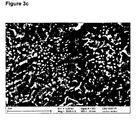
- the layers formed according to this invention may appear in form of more or less homogeneous thin layers (which do not show specific features in SEM due to their nanoscopic size) - see figure 3a - with only a small number of distinct particles of small size, or can occur in form of layers mainly consisting of distinct particles (see the SEM image in Figure 3c )
- Figure 3b shows an example of a coating according to the second aspect of the invention. Also here, no special features can be seen on the surface (apart from the copper crystal structure underneath the thin layer deposit).
- dispersion media organic solvents, preferably organic solvents miscible with water, water and mixtures thereof are suitable.
- Preferred solvents miscible with water are alcohols, in particular alcohols with a boiling point of more than 100°C and preferably below 250°C.
- Water and aqueous solvents are preferred as the dispersion medium. These are advantageous not only with regard to emissions and the non-wetting of the solder stop lacquer; it has also been found that water and aqueous solvents yield better results. This was surprising in that oxidation processes on copper proceed particularly rapidly in an aqueous environment. Solder stop lacquer is used to mask the areas of the printed circuit board which must not be wetted by the solder during the assembly process. The solder stop lacquer should not be wetted by the conductive polymer, since otherwise this would cause short circuits between the copper surfaces.
- dispersions which contain no formic acid or acetic acid are used, however, other acids and/or buffers can be contained in the dispersions.
- dispersions produced commercially by Ormecon GmbH are suitable for reaction with precious or semiprecious metal ions and for reformulation into dispersions which can deposit homogeneous layers in the shortest possible time.
- the dispersions D 1021, D 1022, OMP 7000 and OMN 7100 or 7200 from Ormecon GmbH are particularly suitable as starting dispersions.
- OMN 7100 and D 1022 are preferred. Both are aqueous dispersions with approximately 0.5 % organic metal.
- the doping agent is not critical. Para-toluene sulfonic acid, methane sulfonic acid or polystyrene sulfonic acid are preferred. Mixtures thereof may also be used.
- the dispersions of the conductive polymer(s) or organic metals and the solutions of the precious/semiprecious metal(s) can be used separately in succession, wherein the conductive polymer dispersion serves as a pre-treatment and the precious/semiprecious metal is then deposited on the Cu surface pre-treated with the conductive polymer/organic metal.
- coated articles according to the invention are characterized in particular in that they can not only be soldered well even after prolonged storage, but are also solderable several times, i.e. can be used in multistage soldering processes, so-called reflow processes. In this respect, the properties of (much thicker) metallic coatings were reached or exceeded.
- the new coating in particular that of the second aspect, is superior to all other known surface finishings.
- the colour does hardly change.
- the original colour is a mat silver-grey with copper-colour shining through, however, the copper red being significantly reduced). It merely becomes a bit darker.
- reflow tests even after 10 reflow steps, there was no decrease in the solderability.
- a layer prepared by the preferred method of the present invention shows clearly better aging properties.
- Ag layers of nanometer thickness prepared according to methods known in the prior art are hardly resistant against aging and the initially good conductivity decreases quickly. This does not happen to the coatings of the present invention.
- the surface and the deposition are favourably influenced by the organic nanometal (the conductive polymer).
- the dispersions according to the invention as herein defined can also be used to protect copper powders against oxidation, wherein the copper powder particles have a size in the micrometer range or submicrometer range, i.e. smaller than 1 ⁇ m.
- Example 1 Production of coated printed circuit board according to the first aspect of the invention
- Epoxy resin composite printed circuit boards were cleaned and degreased using a normal commercial cleaner based on sulphuric acid and citric acid (ACL 7001, Ormecon GmbH) in a cleaning bath for 2 minutes at 45°C.
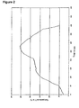
- the printed circuit boards used had a test design (see Figure 1 ), which has been agreed with test institutes and printed circuit board manufacturers and is modelled on real printed circuit board structures. These boards enable the solderability to be measured and assessed.
- the printed circuit boards were rinsed with tap-water at room temperature and then treated with an H 2 O 2 -containing etching solution (Etch 7000, Ormecon GmbH) for 2 minutes at 30°C.
- the boards were again rinsed with tap-water at room temperature and then coated with AgNO 3 with a dispersion according to the invention in the form of OMN 7100.
- the boards were immersed in the aqueous dispersion at room temperature for 1 minute. After this, the printed circuit boards were dried at 45 to 75°C.
- Example 2 Production of coated printed circuit boards with OMN 7100
- Printed circuit boards were coated analogously to Example 1, but wherein the dispersion OMN 7100 used contained no AgNO 3 .
- Table 1 Appearance of the coatings
- Example Active ingredient in dispersion Appearance of the treated boards 1 OMN 7100 with AgNO3 silvery with a copper colour showing through 2 comparative test OMN 7100 freshly copper-coloured 3 comparative test OSP 1 freshly copper-coloured 4 comparative test OSP 2 freshly copper-coloured
- the boards were subjected to a reflow test.
- the board was subjected in a commercial reflow oven to a heat profile (as shown in Figure 2 ) which was used for modern lead-free soldering methods.
- the reflow cycles served for the simulation of repeated soldering operations.
- the soldering angle was then measured by means of a soldering balance.
- Example 6 Production of coated printed circuit board according to the second aspect of the invention
- Epoxy resin composite printed circuit boards were cleaned and degreased as described in Example 1.
- the printed circuit boards used had a test design and were rinsed with tap-water at room temperature and then treated with an H 2 O 2 -containing etching solution as described in Example 1. After etching, the boards were again rinsed with tap-water at room temperature and then coated with a dispersion according to the invention in the form of OMN 7100 containing AgNO 3 in a concentration of 200 mg/l. For this purpose, the boards were immersed in the aqueous dispersion at a temperature of 35 °C for 90 s. After this, the printed circuit boards were dried at temperatures of up to 100 °C.
- Example 7 Production of coated printed circuit boards with OMN 7100
- Printed circuit boards were coated analogously to Example 1, but wherein the dispersion OMN 7100 used contained no AgNO 3 .
- Example 7 printed circuit boards were coated with normal commercial agents based on benzotriazole in accordance with the respective use instructions (Shikoku Co., Japan).
- Example 3 Experiment Reflow-steps Soldering Angle A(°) WA after 85°C/85% rel moisture 16 hr WA after aging at 155°C/4h
- Example 7 0 15-20 70 25-30 1 20-25 70 25-30 2 25-30 25-30 3 20-30 30-35 4 30-35 30-40 5-10 30-40
- Example 8 (Comparison "OM Nanofinish") 0 20-30 45-60 1 30-50 70-80 2 35-70 65-80 3 65-70 110-130 4 75-85 - For Comparison ORMECON CSN 0 15 80 20 1 25 >90 30 2 30 35 3 45 50 4 60 70
- Example 9 (Comparison) Conventional OSP 0 25-30 >90 1 40-50 >90 2 65-70 >90 3 >90 >90 4 >90
- Polyaniline powder was synthesized by oxidative polymerization of aniline in the presence of p-toluene sulfonic acid as dopant as described in WO-A-89/02155 .
- the resulting green polymer powder had a conductivity of 5 S/cm measured as a pressed pellet (10 t pressure at room temperature for 5 minutes).
- a polyaniline dispersion in water was created following reference.
- the dispersion had a particle size of 55 nm (measured by Laser Doppler technique) and showed a conductivity of 180 S/cm when deposited as a homogeneous layer on a glass substrate.
- Dispersing and surface active agents to improve soldering and AgNO3 (150 mg/l) were added to the dispersion. After thorough mixing the dispersion is ready to use.
- the process of providing a solderable surface finish for PCBs using the organic metal / silver nanoparticle finish is a procedure starting with an acid cleaning, followed by a microetch pretreatment step and then by the deposition of the active organic metal / silver layer, ending with rinsing and drying of the PCB.
- the OM/Ag dispersion deposition was carried out at 35°C for 90 sec.
- the PCB is pretreated by a dispersion containing polyaniline (1).
- the board is cleaned using an acidic solution (2), followed by two rinsing steps (3 & 4) in water.
- An acidic solution is used as a conditioner (5).
- the organic metal / silver nanolayer is deposited on the PCB using the aqueous dispersion of polyaniline containing a silver salt (6). After that the PCB is rinsed twice in water (7 & 8) and dried (9).
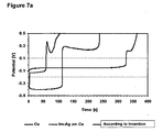
- GCM galvanostatic coulometric measurement
- the potential of the electrode moves to values characteristic of the couple Me A /Me A n+ .
- the potential at the electrode will rapidly change towards more positive values until a second oxidation process can start at the new interface Me B (intermetallic phase or second metal) .
- Equation (1) does not hold if secondary reactions occur and the current is not exclusively used for oxidation of Me A or the reduction of oxides.
- the electrochemical cell consisted of a working electrode with a 0.25 cm 2 area, designed specifically for the evaluation of layer thickness, a platinum wire counter electrode and a reference electrode (Ag/AgCl in 3 mol KCl).
- the test electrolyte was filled into a 50 ml glass body with three 14.5/23 standard tapers and the electrodes are mounted with taper joints.
- the electrolyte used was a water based solution of potassium thiocyanate. The electrolyte was not deaerated.
- the finish of the copper surface in dependence on the immersion time in organic metal / silver nanoparticle finish is displayed in figure 8 .
- the potentials indicate that the amount of free copper surface decreases slowly at the beginning of the process, having the highest rate between 40 and 60 s immersion time and after 60 s the rest of the free copper surface is coated slowly. After about 90 s there is no free copper detectable.
- Figure 3 shows a scanning electron microscopy (SEM) image of copper pad of a PCB after treatment with the organic metal / silver nanoparticle finish.
- SEM scanning electron microscopy
- XPS x-ray photoelectron spectroscopy
- Quantitative information about the surface composition was calculated from survey spectra using the standard Scofield sensitivity factors ( J.H. Scofield, Journal of Electron Spectroscopy and Related Phenomena 8, 129, (1976 )).
- the error can be estimated to be typically ⁇ 10 %; statistic errors of single measurements were calculated using the method of Harrison and Hazell (SIA, 18, 1992, p. 368 - 376 ).
- the surface potentials of copper, oxidized copper, silver on copper after immersion and organic metal / silver nanoparticle finish on copper after immersion were determined using a scanning kelvin probe (SKP, UBM Messtechnik GmbH, Ettlingen, Germany).
- the volta-potential measured with a kelvin sensor is suitable for non-contact measurements of surface potentials ( M. Stratmann, H. Streckel and R. Feser, Corros. Sci. 32, 467 (1991 )).
- the measured object, the working electrode, and the reference electrode of the Kelvin probe form, due to the small gap between them, a capacitor.
- the amplitude of the potential developed between them shows the degree of surface activity.
- a periodic variation in separation by means of an actuator built into the sensor changes the capacitance of the set-up.
- the resulting signal is converted to a measurement signal by means of a lock-in amplifier (Information brochure of UBM Messtechnik GmbH, Ettlingen (1996)).
- the volta-potential difference is directly determined by the surface potential ( M. Stratmann, M. Wolpers, H. Streckel and R. Feser, Ber. Bunsenges. Phys. Chem. 95, 1365 (1991 )).
- tungsten wire with a tip diameter of 80 ⁇ m was used.
- the tip was positioned about 25 ⁇ m above the specimen, the vibration amplitude was ⁇ 10 ⁇ m and the vibration frequency of the needle was 1.75 kHz.
- gold was used as reliable reference material.
- Kelvin potentials of different treated and untreated copper surfaces are summarized in Table 4.
- Table 4 Kelvin potentials of different surfaces Surface Kelvin potential [mV] Cu (pure, unoxidized) 70 Cu oxides 150 - 180 Cu treated with organic metal / silver nanoparticle finish (50 nm layer) 320 - 340 Cu treated with immersion silver (500 nm layer) 400
- the thermal aging was performed to simulate soldering and storage conditions.
- test panels on which the PAni-Ag complex had been deposited under standard conditions were aged up to 4 times in the reflow oven RO 300 FC N2 from Essemtec, Swizerland.
- a lead free soldering profile was chosen with a peak temperature - 250°C.
- To simulate storage conditions other test panels were aged 4h at 155°C in the IR hot air oven Techno HA-06 from Athelec.
- the solderability measurements were preformed using the wetting balance Meniscograph ST60 from Metronelec with appropriate test panels on which the Pani-Ag complex had been deposited under standard conditions. The solderability of the panels was determined as wetting angle under lead free soldering conditions. The solder Sn 95 . 5 Ag 3 . 8 CU 0 . 7 (260 °C) from Ecoloy and fluxer 959 T from Kester were used. The measurement data was converted to wetting angle using the software from Metronelec according to the standard NF-A-89 400P.
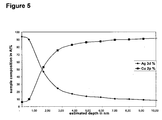
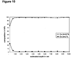
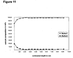
- the XPS showed a very small amount of the Cu surface atoms to be in oxidized stage even after thermal ageing under ambient atmosphere ( Fig. 11 and 12 ), only around 20 - 25%, and ageing does not change the degree of oxidation. Also, during ageing, the Ag did not migrate into the Cu ( Fig. 9 and 10 ).
- Figure 14 shows a printed circuit board before treatment, directly after the surface coating (i.e. surface finish) with organic metal / silver nanoparticle finish and the surface after treatment and aging.
Landscapes
- Engineering & Computer Science (AREA)
- Microelectronics & Electronic Packaging (AREA)
- Manufacturing & Machinery (AREA)
- Chemical & Material Sciences (AREA)
- Materials Engineering (AREA)
- Metallurgy (AREA)
- Organic Chemistry (AREA)
- Electrochemistry (AREA)
- Chemical Kinetics & Catalysis (AREA)
- Laminated Bodies (AREA)
- Parts Printed On Printed Circuit Boards (AREA)
- Preventing Corrosion Or Incrustation Of Metals (AREA)
- Manufacturing Of Printed Wiring (AREA)
- Non-Insulated Conductors (AREA)
- Manufacturing Of Electric Cables (AREA)
- Other Surface Treatments For Metallic Materials (AREA)
Claims (16)
- Beschichteter Artikel, der eine Leiterplatte ist, die(i) mindestens eine elektrisch leitende Basisschicht,(ii) mindestens eine Schicht aus Kupfer und/oder einer Kupferlegierung, und(iii) eine Schicht, die aus mindestens einem elektrisch leitfähigen Polymer, wobei das elektrisch leitfähige Polymer aus Polyanilin (PAni), Polythiophen (PTh), Polypyrrol (PPy), Poly (3,4-Ethylendioxythiophen (PEDT), Polythienothiophen (PTT), deren Derivaten und Mischungen davon ausgewählt ist, und mindestens einem dispergierten Edelmetall ausgewählt aus der Gruppe bestehend aus Ag, Au, Pd, Pt, Rh, Ir, Ru, Os und Re oder mindestens einem dispergierten Halbedelmetall ausgewählt aus der Gruppe bestehend aus Ni, Ti, Cu und Bi, oder einer Mischung davon, und gegebenenfalls weiteren Bestandteilen ausgewählt aus elektrisch nicht leitfähigen Bestandteilen und Komplexierungsmitteln besteht,aufweist, wobei die Kupfer- oder Kupferlegierungsschicht (ii) zwischen der Basisschicht (i) und Schicht (iii) angeordnet ist, die das leitfähige Polymer enthält, und wobei Schicht (iii) eine lötfähige Oberflächenbeschichtung darstellt.
- Beschichteter Artikel nach Anspruch 1, wobei das Edelmetall ausgewählt ist aus der Gruppe bestehend aus Ag und Au und insbesondere Ag ist, und wobei das Halbedelmetall ausgewählt ist aus der Gruppe bestehend aus Ni und Ti.
- Beschichteter Artikel nach Anspruch 1 oder Anspruch 2, wobei Schicht (iii) eine Schichtdicke von 10 nm bis 1 µm aufweist, insbesondere weniger als 500 nm oder weniger als 200 nm.
- Beschichteter Artikel nach einem der vorhergehenden Ansprüche, wobei Schicht (iii) 5% bis 45% leitfähiges Polymer und 5 bis 45% (Halb)Edelmetall enthält, bezogen auf die Masse von Schicht (iii).
- Beschichteter Artikel nach Anspruch 1, wobei Schicht (iii) eine nanoskopische Schicht mit einer durchschnittlichen Dicke von 100 nm oder weniger ist, wobei die Schicht mindestens 80 Gew.%, bezogen auf Schicht (iii), des mindestens einen Edelmetalls und/oder Halbedelmetalls aufweist, das von Kupfer verschieden ist.
- Beschichteter Artikel nach Anspruch 5, wobei Schicht (iii) eine durchschnittliche Dicke von 2 bis 100 nm oder weniger als 10 nm aufweist.
- Beschichteter Artikel nach einem der vorhergehenden Ansprüche, bei dem Schicht (iii) ferner mindestens einen elektrisch nicht leitfähigen Anteil enthält, vorzugsweise ein elektrisch nicht leitfähiges Polymer.
- Beschichteter Artikel nach einem der vorhergehenden Ansprüche, wobei Schicht (iii) mindestens ein Komplexierungsmittel, insbesondere ein Kupferkomplexierungsmittel enthält, wobei das Mittel vorzugsweise ausgewählt ist aus Benzimidazolen, Imidazolen, Benzotriazolen, Harnstoff, Thioharnstoff, Imidazol-2-thionen, (Natrium)ethylendiamintetraacetat (EDTA), (K-, Na-)Tartraten, Ethylendiamin-Bernsteinsäure und Mischungen davon.
- Beschichteter Artikel nach einem der vorhergehenden Ansprüche, wobei die Basisschicht (i) Epoxid, Epoxidverbundmaterial, Teflon, Cyanidester, Keramik, Cellulose, Celluloseverbundmaterial, Pappe und/oder Polyimid enthält.
- Beschichteter Artikel nach einem der vorhergehenden Ansprüche, wobei die Basisschicht (i) eine Schichtdicke von 0.1 bis 3 mm aufweist und/oder wobei Schicht (ii) eine Schichtdicke von 5 bis 210 µm aufweist.
- Beschichteter Artikel nach einem der vorhergehenden Ansprüche, der ferner eine Metall- oder Legierungsschicht (iv) enthält, die zwischen Schicht (ii) und Schicht (iii) angeordnet ist, und die insbesondere Silber, Zinn, Gold, Palladium oder Platin enthält und vorzugsweise eine Schichtdicke von 10 bis 800 nm aufweist.
- Verfahren zur Herstellung einer Leiterplatte gemäß einem der vorhergehenden Ansprüche, bei dem(1) man auf die Oberfläche einer Basisschicht eine Schicht aus Kupfer oder einer kupferhaltigen Legierung aufbringt,(2) man die in Schritt (1) hergestellt Schicht strukturiert und(3) man auf die strukturierte Kupfer- oder Kupferlegierungsschicht eine Schicht aufbringt, die aus mindestens einem elektrisch leitfähigem Polymer, wobei das elektrisch leitfähige Polymer ausgewählt ist aus Polyanilin (PAni), Polythiophen (PTh), Polypyrrol (PPy), Poly(3,4-Ethylendioxythiophen) (PEDT), Polythienothiophen (PTT), Derivaten davon und Mischungen davon, und mindestens einem dispergierten Edelmetall ausgewählt aus der Gruppe bestehend aus Ag, Au, Pd, Pt, Rh, Ir, Ru, Os und Re und/oder mindestens einem dispergierten Halbedelmetall ausgewählt aus der Gruppe bestehend aus Ni, Ti, Cu und Bi oder einer Mischung davon und gegebenenfalls weiteren Bestandteilen ausgewählt aus elektrisch nicht leitfähigen Bestandteilen und Komplexierungsmitteln besteht, wobei die Schicht eine lötfähige Oberflächenbeschichtung ergibt.
- Verfahren nach Anspruch 12, bei dem das Edelmetall ausgewählt ist aus der Gruppe bestehend aus Ag und Au und insbesondere Ag ist und wobei das Halbedelmetall ausgewählt ist aus der Gruppe bestehend aus Ni und Ti.
- Verfahren nach einem der Ansprüche 12 oder 13, wobei die Kupfer- oder Kupferlegierungsschicht (ii) im Anschluss an Schritt (1) einer Reinigung unterzogen wird und/oder wobei die Kupfer- oder Kupferlegierungsschicht (ii) im Anschluss an Schritt (1) oder nach der Reinigung einer oxidativen Vorbehandlung unterzogen wird.
- Verwendung einer Dispersion, die aus einem Dispersionsmedium, das bei Raumtemperatur flüssig ist, mindestens einem elektrisch leitfähigen Polymer, wobei das elektrisch leitfähige Polymer ausgewählt ist aus Polyanilin (PAni), Polythiophen (PTh), Polypyrrol (PPy), Poly(3,4-Ethylendioxythiophen) (PEDT), Polythienothiophen (PTT), Derivaten davon und Mischungen davon und mindestens einem Edelmetall ausgewählt aus der Gruppe bestehend aus Ag, Au, Pd, Pt, Rh, Ir, Ru, Os und Re und/oder Halbedelmetall ausgewählt aus der Gruppe bestehend aus Ni, Ti, Cu und Bi und gegebenenfalls mindestens einem weiteren Bestandteil, der ausgewählt ist aus elektrisch nicht leitfähigen Bestandteilen, Komplexierungsmitteln, Viskositätsmodifizierungsmitteln, Fließhilfen, Trocknungshilfen, Glanzverbesserern, Mattierungsmitteln und Mischungen davon besteht, zur Verhinderung der Korrosion und/oder zur Verhinderung eines Verlustes der Lötfähigkeit von Leiterplatten.
- Verwendung nach Anspruch 15, wobei das Dispersionsmittel Wasser, ein mit Wasser mischbares organisches Lösungsmittel oder eine Mischung davon enthält.
Applications Claiming Priority (3)
| Application Number | Priority Date | Filing Date | Title |
|---|---|---|---|
| DE200610043811 DE102006043811B4 (de) | 2006-09-13 | 2006-09-13 | Artikel mit einer Beschichtung von elektrisch leitfähigem Polymer und Edel-/Halbedelmetall sowie Verfahren zu deren Herstellung |
| DE102006047501 | 2006-10-05 | ||
| PCT/EP2007/007467 WO2008031492A1 (en) | 2006-09-13 | 2007-08-24 | Article with a coating of electrically conductive polymer and precious/semiprecious metal and process for production thereof |
Publications (2)
| Publication Number | Publication Date |
|---|---|
| EP2062467A1 EP2062467A1 (de) | 2009-05-27 |
| EP2062467B1 true EP2062467B1 (de) | 2012-02-15 |
Family
ID=38799833
Family Applications (1)
| Application Number | Title | Priority Date | Filing Date |
|---|---|---|---|
| EP07801892A Not-in-force EP2062467B1 (de) | 2006-09-13 | 2007-08-24 | Artikel mit beschichtung aus elektrisch leitendem polymer und edel-/halbedelmetal sowie herstellungsverfahren dafür |
Country Status (9)
| Country | Link |
|---|---|
| US (1) | US8153271B2 (de) |
| EP (1) | EP2062467B1 (de) |
| JP (1) | JP5114714B2 (de) |
| KR (1) | KR101422529B1 (de) |
| AT (1) | ATE546032T1 (de) |
| CA (1) | CA2662851A1 (de) |
| MY (1) | MY147793A (de) |
| TW (1) | TWI420994B (de) |
| WO (1) | WO2008031492A1 (de) |
Cited By (1)
| Publication number | Priority date | Publication date | Assignee | Title |
|---|---|---|---|---|
| US9865952B2 (en) | 2015-12-22 | 2018-01-09 | Continental Automotive Gmbh | Plug contact with organic coating and printed circuit board arrangement |
Families Citing this family (13)
| Publication number | Priority date | Publication date | Assignee | Title |
|---|---|---|---|---|
| DE102004003784B4 (de) * | 2004-01-23 | 2011-01-13 | Ormecon Gmbh | Dispersion intrinsisch leitfähigen Polyanilins und deren Verwendung |
| DE102004030388A1 (de) * | 2004-06-23 | 2006-01-26 | Ormecon Gmbh | Artikel mit einer Beschichtung von elektrisch leitfähigem Polymer und Verfahren zu deren Herstellung |
| DE102005010162B4 (de) * | 2005-03-02 | 2007-06-14 | Ormecon Gmbh | Leitfähige Polymere aus Teilchen mit anisotroper Morphologie |
| DE102005039608A1 (de) * | 2005-08-19 | 2007-03-01 | Ormecon Gmbh | Zusammensetzung mit intrinsisch leitfähigem Polymer |
| US8026168B2 (en) | 2007-08-15 | 2011-09-27 | Tokyo Electron Limited | Semiconductor device containing an aluminum tantalum carbonitride barrier film and method of forming |
| US7985680B2 (en) | 2008-08-25 | 2011-07-26 | Tokyo Electron Limited | Method of forming aluminum-doped metal carbonitride gate electrodes |
| EP2417241A4 (de) * | 2009-04-08 | 2014-10-15 | Sunsonix | Verfahren und vorrichtung zur entfernung von kontaminationsmaterial aus substraten |
| DE102012017058A1 (de) | 2012-08-29 | 2014-03-06 | BWSI GmbH & Co. KG | Chemische Beschichtungsanlagen mit turbulenzarmer Strömung |
| WO2014023745A1 (en) | 2012-08-07 | 2014-02-13 | Bwsi Gmbh & Co Kg | Chemical coating unit with low-turbulence flow |
| DE102012015459A1 (de) | 2012-08-07 | 2014-02-13 | BWSI GmbH & Co. KG | Chemische Beschichtungsanlage mit turbulenzarmer Strömung |
| CN105543766B (zh) * | 2016-01-07 | 2019-02-26 | 山东省特种设备检验研究院泰安分院 | NiTi合金复合涂层及其制备方法 |
| CN112992425B (zh) * | 2021-02-24 | 2022-08-30 | 烟台万隆真空冶金股份有限公司 | 一种梯度结构铜基复合电接触材料的制备方法 |
| CN114025474B (zh) * | 2021-11-22 | 2022-07-19 | 百强电子(深圳)有限公司 | 印刷电路板及其制造方法 |
Family Cites Families (75)
| Publication number | Priority date | Publication date | Assignee | Title |
|---|---|---|---|---|
| US3977756A (en) | 1975-09-22 | 1976-08-31 | General Motors Corporation | Transitional connector for printed circuits |
| US4394498A (en) | 1981-08-24 | 1983-07-19 | Celanese Corporation | Method for providing particulates of liquid crystal polymers and particulates produced therefrom |
| AT378008B (de) | 1982-09-07 | 1985-06-10 | Neumayer Karl Gmbh | Verfahren zur herstellung von mit einer zinnlegierung ueberzogenen draehten |
| US4585695A (en) | 1983-10-11 | 1986-04-29 | Agency Of Industrial Science And Technology | Electrically conductive polypyrrole article |
| DE3440617C1 (de) | 1984-11-07 | 1986-06-26 | Zipperling Kessler & Co (Gmbh & Co), 2070 Ahrensburg | Antistatische bzw. elektrisch halbleitende thermoplastische Polymerblends,Verfahren zu deren Herstellung und deren Verwendung |
| US4657632A (en) | 1985-08-29 | 1987-04-14 | Techno Instruments Investments 1983 Ltd. | Use of immersion tin coating as etch resist |
| US5104599A (en) | 1987-03-05 | 1992-04-14 | Allied-Signal Inc. | Method of forming short fibers composed of anisotropic polymers |
| DE3729566A1 (de) | 1987-09-04 | 1989-03-16 | Zipperling Kessler & Co | Intrinsisch leitfaehiges polymer in form eines dispergierbaren feststoffes, dessen herstellung und dessen verwendung |
| CA1339210C (en) * | 1988-05-31 | 1997-08-05 | John Lewicki | Recombinant techniques for production of novel natriuretic and vasodilator peptides |
| US5498761A (en) | 1988-10-11 | 1996-03-12 | Wessling; Bernhard | Process for producing thin layers of conductive polymers |
| EP0407492B1 (de) | 1988-10-11 | 1997-07-30 | Zipperling Kessler & Co (GmbH & Co) | Verfahren zur herstellung dünner schichten aus leitfähigen polymeren |
| US4959180A (en) | 1989-02-03 | 1990-09-25 | The United States Of America As Represented By The United States Department Of Energy | Colloidal polyaniline |
| EP0466943A4 (en) | 1990-02-05 | 1992-07-01 | Vsesojuzny Nauchno-Issledovatelsky Instrumentalny Institut | Liquid pulverizer |
| US5173766A (en) | 1990-06-25 | 1992-12-22 | Lsi Logic Corporation | Semiconductor device package and method of making such a package |
| US5192835A (en) | 1990-10-09 | 1993-03-09 | Eastman Kodak Company | Bonding of solid state device to terminal board |
| US5278213A (en) | 1991-04-22 | 1994-01-11 | Allied Signal Inc. | Method of processing neutral polyanilines in solvent and solvent mixtures |
| US5281363A (en) | 1991-04-22 | 1994-01-25 | Allied-Signal Inc. | Polyaniline compositions having a surface/core dopant arrangement |
| DE4238765A1 (de) | 1992-11-10 | 1994-05-11 | Stuebing Gmbh | Verfahren zur stromlosen Verzinnung von Leiterplatten und deren Verwendung |
| DE4317010A1 (de) | 1993-05-17 | 1994-11-24 | Zipperling Kessler & Co | Dispergierbares intrinsisch leitfähiges Polymer und Verfahren zu dessen Herstellung |
| JP2536817B2 (ja) | 1993-06-25 | 1996-09-25 | ツイッパーリング ケスラー ウント コー(ゲーエムベーハー ウント コー) | 腐食保護された金属材料の製造方法及びこの方法によって得られる材料 |
| US5532025A (en) | 1993-07-23 | 1996-07-02 | Kinlen; Patrick J. | Corrosion inhibiting compositions |
| US5403913A (en) | 1993-08-12 | 1995-04-04 | The Trustees Of The University Of Pennsylvania | Methods for preparing conductive polyanilines |
| DE4333127A1 (de) | 1993-09-29 | 1995-03-30 | Basf Ag | Verfahren zum Schutz von lötfähigen Kupfer- und Kupferlegierungsoberflächen vor Korrosion |
| US5682043A (en) | 1994-06-28 | 1997-10-28 | Uniax Corporation | Electrochemical light-emitting devices |
| US5595689A (en) | 1994-07-21 | 1997-01-21 | Americhem, Inc. | Highly conductive polymer blends with intrinsically conductive polymers |
| US5700398A (en) | 1994-12-14 | 1997-12-23 | International Business Machines Corporation | Composition containing a polymer and conductive filler and use thereof |
| US5645890A (en) | 1995-02-14 | 1997-07-08 | The Trustess Of The University Of Pennsylvania | Prevention of corrosion with polyaniline |
| DE19525708C1 (de) | 1995-07-14 | 1997-01-30 | Rmh Polymers Gmbh & Co Kg | Temporärer Anlaufschutz für Kupfer und Kupferlegierungen |
| US5846606A (en) | 1995-11-29 | 1998-12-08 | Zipperling Kessler & Co. (Gmbh&Co.) | Process for the production of metallized materials |
| US5733599A (en) | 1996-03-22 | 1998-03-31 | Macdermid, Incorporated | Method for enhancing the solderability of a surface |
| EP0993512B1 (de) | 1997-06-27 | 2002-08-14 | University Of Southampton | Poröser film und verfahren zu seiner herstellung |
| WO1999005687A1 (de) | 1997-07-25 | 1999-02-04 | Zipperling Kessler & Co. (Gmbh & Co.) | Chemische verbindungen von intrinsisch leitfähigen polymeren mit metallen |
| DE19754221A1 (de) | 1997-12-06 | 1999-06-17 | Federal Mogul Wiesbaden Gmbh | Schichtverbundwerkstoff für Gleitlager mit bleifreier Gleitschicht |
| US6015482A (en) | 1997-12-18 | 2000-01-18 | Circuit Research Corp. | Printed circuit manufacturing process using tin-nickel plating |
| US6123995A (en) | 1998-03-06 | 2000-09-26 | Shipley Company, L.L.C. | Method of manufacture of multilayer circuit boards |
| DE19812258A1 (de) | 1998-03-20 | 1999-09-23 | Bayer Ag | Elektrolumineszierende Anordnungen unter Verwendung von Blendsystemen |
| DE69913605T2 (de) | 1998-06-05 | 2004-09-23 | Teijin Ltd. | Antistatische Polyesterfolie und Verfahren zu ihrer Herstellung |
| JP3937113B2 (ja) | 1998-06-05 | 2007-06-27 | 日産化学工業株式会社 | 有機−無機複合導電性ゾル及びその製造法 |
| JP3796381B2 (ja) | 1999-01-26 | 2006-07-12 | 株式会社エスアイアイ・マイクロパーツ | 電気二重層キャパシタ |
| US6593399B1 (en) | 1999-06-04 | 2003-07-15 | Rohm And Haas Company | Preparing conductive polymers in the presence of emulsion latexes |
| US6821323B1 (en) | 1999-11-12 | 2004-11-23 | Enthone Inc. | Process for the non-galvanic tin plating of copper or copper alloys |
| US6361823B1 (en) | 1999-12-03 | 2002-03-26 | Atotech Deutschland Gmbh | Process for whisker-free aqueous electroless tin plating |
| US6706418B2 (en) | 2000-07-01 | 2004-03-16 | Shipley Company L.L.C. | Metal alloy compositions and plating methods related thereto |
| US6730401B2 (en) | 2001-03-16 | 2004-05-04 | Eastman Chemical Company | Multilayered packaging materials for electrostatic applications |
| JP2003049293A (ja) | 2001-03-16 | 2003-02-21 | Shipley Co Llc | 錫メッキ |
| JP2002289653A (ja) | 2001-03-26 | 2002-10-04 | Hitachi Cable Ltd | 半導体装置用テープキャリアおよびその製造方法 |
| US6824857B2 (en) * | 2001-04-02 | 2004-11-30 | Nashua Corporation | Circuit elements having an embedded conductive trace and methods of manufacture |
| CN101330800B (zh) | 2001-07-19 | 2011-03-23 | 东丽株式会社 | 电路基板的制造方法 |
| JP2005502192A (ja) | 2001-08-22 | 2005-01-20 | ワールド プロパティーズ インク. | 回路基板の金属への接着を改善する方法及びその方法で製作された物品 |
| GB2380964B (en) | 2001-09-04 | 2005-01-12 | Multicore Solders Ltd | Lead-free solder paste |
| JP3513709B2 (ja) | 2001-10-16 | 2004-03-31 | 石原薬品株式会社 | 前処理によるスズホイスカーの防止方法 |
| TW200302685A (en) | 2002-01-23 | 2003-08-01 | Matsushita Electric Industrial Co Ltd | Circuit component built-in module and method of manufacturing the same |
| KR20040096630A (ko) | 2002-03-01 | 2004-11-16 | 이 아이 듀폰 디 네모아 앤드 캄파니 | 첨가제를 함유하는 유기 전도성 중합체의 인쇄 |
| JP3940620B2 (ja) | 2002-03-22 | 2007-07-04 | ガンツ化成株式会社 | 非球塊状ポリマー微粒子の製造法 |
| JP3855161B2 (ja) | 2002-05-10 | 2006-12-06 | 石原薬品株式会社 | 電子部品のスズホイスカーの防止方法 |
| DE10227362A1 (de) | 2002-06-19 | 2004-01-08 | Basf Ag | Komplexbildner für die Behandlung von Metall- und Kunstoffoberflächen |
| DE10234363A1 (de) * | 2002-07-27 | 2004-02-12 | Robert Bosch Gmbh | Korrosionsschutzlack für metallische Oberflächen |
| EP1549696A1 (de) | 2002-09-24 | 2005-07-06 | E.I. Du Pont De Nemours And Company | Mit polymersüurekolloiden hergestellte wasserdispergierbare polyaniline für elektronikanwendungen |
| ATE404609T1 (de) | 2002-09-24 | 2008-08-15 | Du Pont | Wasserdispergierbare polythiophene hergestellt unter verwendung von kolloiden auf basis von polymersäuren |
| EP2341118A1 (de) * | 2002-09-24 | 2011-07-06 | E. I. du Pont de Nemours and Company | Elektrisch leitfähige Kompositwerkstoffe basierend auf organischen Polymeren und Nanoteilchen sowie deren Verwendung |
| US6962642B2 (en) | 2002-09-26 | 2005-11-08 | International Business Machines Corporation | Treating copper surfaces for electronic applications |
| US20040191605A1 (en) | 2002-12-27 | 2004-09-30 | Foamex L.P. | Gas diffusion layer containing inherently conductive polymer for fuel cells |
| JP4603812B2 (ja) | 2003-05-12 | 2010-12-22 | ローム・アンド・ハース・エレクトロニック・マテリアルズ,エル.エル.シー. | 改良されたスズめっき方法 |
| AT412094B (de) | 2003-05-13 | 2004-09-27 | Austria Tech & System Tech | Verfahren zur beschichtung von rohlingen zur herstellung von gedruckten leiterplatten (pcb) |
| DE102004003784B4 (de) | 2004-01-23 | 2011-01-13 | Ormecon Gmbh | Dispersion intrinsisch leitfähigen Polyanilins und deren Verwendung |
| JP5245188B2 (ja) | 2004-03-03 | 2013-07-24 | 日清紡ホールディングス株式会社 | 楕円球状有機ポリマー粒子およびその製造方法 |
| EP1730215B1 (de) | 2004-03-18 | 2017-08-16 | Enthone GmbH | Zusammensetzung, die ein leitfähiges polymer in kolloidaler form und kohlenstoff enthält |
| US20050269555A1 (en) | 2004-05-11 | 2005-12-08 | Suck-Hyun Lee | Conductive polymers having highly enhanced solubility in organic solvent and electrical conductivity and synthesizing process thereof |
| DE102004030388A1 (de) | 2004-06-23 | 2006-01-26 | Ormecon Gmbh | Artikel mit einer Beschichtung von elektrisch leitfähigem Polymer und Verfahren zu deren Herstellung |
| DE102004030930A1 (de) * | 2004-06-25 | 2006-02-23 | Ormecon Gmbh | Zinnbeschichtete Leiterplatten mit geringer Neigung zur Whiskerbildung |
| US7087441B2 (en) | 2004-10-21 | 2006-08-08 | Endicott Interconnect Technologies, Inc. | Method of making a circuitized substrate having a plurality of solder connection sites thereon |
| DE102005010162B4 (de) | 2005-03-02 | 2007-06-14 | Ormecon Gmbh | Leitfähige Polymere aus Teilchen mit anisotroper Morphologie |
| DE202005010364U1 (de) * | 2005-07-01 | 2005-09-08 | Ormecon Gmbh | Zinnbeschichtete flexible Leiterplatten mit geringer Neigung zur Whiskerbildung |
| DE102005039608A1 (de) * | 2005-08-19 | 2007-03-01 | Ormecon Gmbh | Zusammensetzung mit intrinsisch leitfähigem Polymer |
| DE102007040065A1 (de) | 2007-08-24 | 2009-02-26 | Ormecon Gmbh | Artikel mit einer nanoskopischen Beschichtung aus Edel-/Halbedelmetall sowie Verfahren zu deren Herstellung |
-
2007
- 2007-08-24 WO PCT/EP2007/007467 patent/WO2008031492A1/en not_active Ceased
- 2007-08-24 AT AT07801892T patent/ATE546032T1/de active
- 2007-08-24 KR KR1020097007211A patent/KR101422529B1/ko not_active Expired - Fee Related
- 2007-08-24 EP EP07801892A patent/EP2062467B1/de not_active Not-in-force
- 2007-08-24 US US12/439,133 patent/US8153271B2/en not_active Expired - Fee Related
- 2007-08-24 JP JP2009527711A patent/JP5114714B2/ja not_active Expired - Fee Related
- 2007-08-24 CA CA002662851A patent/CA2662851A1/en not_active Abandoned
- 2007-08-24 MY MYPI20090991A patent/MY147793A/en unknown
- 2007-08-27 TW TW096131658A patent/TWI420994B/zh not_active IP Right Cessation
Cited By (1)
| Publication number | Priority date | Publication date | Assignee | Title |
|---|---|---|---|---|
| US9865952B2 (en) | 2015-12-22 | 2018-01-09 | Continental Automotive Gmbh | Plug contact with organic coating and printed circuit board arrangement |
Also Published As
| Publication number | Publication date |
|---|---|
| JP2010504225A (ja) | 2010-02-12 |
| KR20090075683A (ko) | 2009-07-08 |
| US20100012359A1 (en) | 2010-01-21 |
| WO2008031492A1 (en) | 2008-03-20 |
| EP2062467A1 (de) | 2009-05-27 |
| TWI420994B (zh) | 2013-12-21 |
| ATE546032T1 (de) | 2012-03-15 |
| MY147793A (en) | 2013-01-31 |
| KR101422529B1 (ko) | 2014-07-24 |
| US8153271B2 (en) | 2012-04-10 |
| JP5114714B2 (ja) | 2013-01-09 |
| TW200822825A (en) | 2008-05-16 |
| WO2008031492A8 (en) | 2009-04-23 |
| CA2662851A1 (en) | 2008-03-20 |
Similar Documents
| Publication | Publication Date | Title |
|---|---|---|
| EP2062467B1 (de) | Artikel mit beschichtung aus elektrisch leitendem polymer und edel-/halbedelmetal sowie herstellungsverfahren dafür | |
| US7547479B2 (en) | Tin-coated printed circuit boards with low tendency to whisker formation | |
| US20070275159A1 (en) | Process for producing an article with a coating of electrically conductive polymer | |
| Yu et al. | Electrochemical migration of Sn-Pb and lead free solder alloys under distilled water | |
| EP1594141A1 (de) | Abschlussbeschichtung zur Verwendung für oberflächenmontierbare Bauelemente | |
| KR100215181B1 (ko) | 도전성 은/증합체 복합체의 부식 및 용해 방지구조물 | |
| CN101524006B (zh) | 具有导电聚合物和贵/半贵金属涂层的制品及其生产方法 | |
| EP1521862A1 (de) | Verfahren zum aussenstromlosen abscheiden von silber | |
| WO2009027016A1 (en) | Article with a nanoscopic coating of precious/semiprecious metal and process for its production | |
| KR100679798B1 (ko) | 커넥터용 접속단자 및 그 표면 처리 방법 | |
| DE202005010364U1 (de) | Zinnbeschichtete flexible Leiterplatten mit geringer Neigung zur Whiskerbildung | |
| Wessling et al. | An organic metal/silver nanoparticle finish on copper for efficient passivation and solderability preservation | |
| Cullen | New Generation Metallic Solderability Preservatives: Immersion Silver Performance Results | |
| KR100405350B1 (ko) | 전자부품용 리드선 및 그 제조방법 | |
| Arendt et al. | Nanotechnology for Lead-Free PWB Final Finishes with the Organic Metal | |
| Baudrand | htroducti on |
Legal Events
| Date | Code | Title | Description |
|---|---|---|---|
| PUAI | Public reference made under article 153(3) epc to a published international application that has entered the european phase |
Free format text: ORIGINAL CODE: 0009012 |
|
| 17P | Request for examination filed |
Effective date: 20090129 |
|
| AK | Designated contracting states |
Kind code of ref document: A1 Designated state(s): AT BE BG CH CY CZ DE DK EE ES FI FR GB GR HU IE IS IT LI LT LU LV MC MT NL PL PT RO SE SI SK TR |
|
| AX | Request for extension of the european patent |
Extension state: AL BA HR MK RS |
|
| 17Q | First examination report despatched |
Effective date: 20100127 |
|
| GRAP | Despatch of communication of intention to grant a patent |
Free format text: ORIGINAL CODE: EPIDOSNIGR1 |
|
| GRAS | Grant fee paid |
Free format text: ORIGINAL CODE: EPIDOSNIGR3 |
|
| RAP1 | Party data changed (applicant data changed or rights of an application transferred) |
Owner name: ENTHONE, INC. |
|
| GRAA | (expected) grant |
Free format text: ORIGINAL CODE: 0009210 |
|
| AK | Designated contracting states |
Kind code of ref document: B1 Designated state(s): AT BE BG CH CY CZ DE DK EE ES FI FR GB GR HU IE IS IT LI LT LU LV MC MT NL PL PT RO SE SI SK TR |
|
| DAX | Request for extension of the european patent (deleted) | ||
| REG | Reference to a national code |
Ref country code: CH Ref legal event code: EP Ref country code: GB Ref legal event code: FG4D |
|
| REG | Reference to a national code |
Ref country code: IE Ref legal event code: FG4D |
|
| REG | Reference to a national code |
Ref country code: AT Ref legal event code: REF Ref document number: 546032 Country of ref document: AT Kind code of ref document: T Effective date: 20120315 |
|
| REG | Reference to a national code |
Ref country code: DE Ref legal event code: R096 Ref document number: 602007020726 Country of ref document: DE Effective date: 20120419 |
|
| REG | Reference to a national code |
Ref country code: NL Ref legal event code: T3 |
|
| LTIE | Lt: invalidation of european patent or patent extension |
Effective date: 20120215 |
|
| PG25 | Lapsed in a contracting state [announced via postgrant information from national office to epo] |
Ref country code: IS Free format text: LAPSE BECAUSE OF FAILURE TO SUBMIT A TRANSLATION OF THE DESCRIPTION OR TO PAY THE FEE WITHIN THE PRESCRIBED TIME-LIMIT Effective date: 20120615 Ref country code: LT Free format text: LAPSE BECAUSE OF FAILURE TO SUBMIT A TRANSLATION OF THE DESCRIPTION OR TO PAY THE FEE WITHIN THE PRESCRIBED TIME-LIMIT Effective date: 20120215 |
|
| PG25 | Lapsed in a contracting state [announced via postgrant information from national office to epo] |
Ref country code: BE Free format text: LAPSE BECAUSE OF FAILURE TO SUBMIT A TRANSLATION OF THE DESCRIPTION OR TO PAY THE FEE WITHIN THE PRESCRIBED TIME-LIMIT Effective date: 20120215 Ref country code: PL Free format text: LAPSE BECAUSE OF FAILURE TO SUBMIT A TRANSLATION OF THE DESCRIPTION OR TO PAY THE FEE WITHIN THE PRESCRIBED TIME-LIMIT Effective date: 20120215 Ref country code: GR Free format text: LAPSE BECAUSE OF FAILURE TO SUBMIT A TRANSLATION OF THE DESCRIPTION OR TO PAY THE FEE WITHIN THE PRESCRIBED TIME-LIMIT Effective date: 20120516 Ref country code: FI Free format text: LAPSE BECAUSE OF FAILURE TO SUBMIT A TRANSLATION OF THE DESCRIPTION OR TO PAY THE FEE WITHIN THE PRESCRIBED TIME-LIMIT Effective date: 20120215 Ref country code: LV Free format text: LAPSE BECAUSE OF FAILURE TO SUBMIT A TRANSLATION OF THE DESCRIPTION OR TO PAY THE FEE WITHIN THE PRESCRIBED TIME-LIMIT Effective date: 20120215 Ref country code: PT Free format text: LAPSE BECAUSE OF FAILURE TO SUBMIT A TRANSLATION OF THE DESCRIPTION OR TO PAY THE FEE WITHIN THE PRESCRIBED TIME-LIMIT Effective date: 20120615 |
|
| REG | Reference to a national code |
Ref country code: AT Ref legal event code: MK05 Ref document number: 546032 Country of ref document: AT Kind code of ref document: T Effective date: 20120215 |
|
| PG25 | Lapsed in a contracting state [announced via postgrant information from national office to epo] |
Ref country code: CY Free format text: LAPSE BECAUSE OF FAILURE TO SUBMIT A TRANSLATION OF THE DESCRIPTION OR TO PAY THE FEE WITHIN THE PRESCRIBED TIME-LIMIT Effective date: 20120215 |
|
| PG25 | Lapsed in a contracting state [announced via postgrant information from national office to epo] |
Ref country code: EE Free format text: LAPSE BECAUSE OF FAILURE TO SUBMIT A TRANSLATION OF THE DESCRIPTION OR TO PAY THE FEE WITHIN THE PRESCRIBED TIME-LIMIT Effective date: 20120215 Ref country code: SE Free format text: LAPSE BECAUSE OF FAILURE TO SUBMIT A TRANSLATION OF THE DESCRIPTION OR TO PAY THE FEE WITHIN THE PRESCRIBED TIME-LIMIT Effective date: 20120215 Ref country code: DK Free format text: LAPSE BECAUSE OF FAILURE TO SUBMIT A TRANSLATION OF THE DESCRIPTION OR TO PAY THE FEE WITHIN THE PRESCRIBED TIME-LIMIT Effective date: 20120215 Ref country code: SI Free format text: LAPSE BECAUSE OF FAILURE TO SUBMIT A TRANSLATION OF THE DESCRIPTION OR TO PAY THE FEE WITHIN THE PRESCRIBED TIME-LIMIT Effective date: 20120215 Ref country code: CZ Free format text: LAPSE BECAUSE OF FAILURE TO SUBMIT A TRANSLATION OF THE DESCRIPTION OR TO PAY THE FEE WITHIN THE PRESCRIBED TIME-LIMIT Effective date: 20120215 Ref country code: RO Free format text: LAPSE BECAUSE OF FAILURE TO SUBMIT A TRANSLATION OF THE DESCRIPTION OR TO PAY THE FEE WITHIN THE PRESCRIBED TIME-LIMIT Effective date: 20120215 |
|
| PG25 | Lapsed in a contracting state [announced via postgrant information from national office to epo] |
Ref country code: SK Free format text: LAPSE BECAUSE OF FAILURE TO SUBMIT A TRANSLATION OF THE DESCRIPTION OR TO PAY THE FEE WITHIN THE PRESCRIBED TIME-LIMIT Effective date: 20120215 |
|
| PLBE | No opposition filed within time limit |
Free format text: ORIGINAL CODE: 0009261 |
|
| STAA | Information on the status of an ep patent application or granted ep patent |
Free format text: STATUS: NO OPPOSITION FILED WITHIN TIME LIMIT |
|
| 26N | No opposition filed |
Effective date: 20121116 |
|
| PG25 | Lapsed in a contracting state [announced via postgrant information from national office to epo] |
Ref country code: AT Free format text: LAPSE BECAUSE OF FAILURE TO SUBMIT A TRANSLATION OF THE DESCRIPTION OR TO PAY THE FEE WITHIN THE PRESCRIBED TIME-LIMIT Effective date: 20120215 |
|
| REG | Reference to a national code |
Ref country code: DE Ref legal event code: R097 Ref document number: 602007020726 Country of ref document: DE Effective date: 20121116 |
|
| REG | Reference to a national code |
Ref country code: CH Ref legal event code: PL |
|
| PG25 | Lapsed in a contracting state [announced via postgrant information from national office to epo] |
Ref country code: MC Free format text: LAPSE BECAUSE OF NON-PAYMENT OF DUE FEES Effective date: 20120831 |
|
| PG25 | Lapsed in a contracting state [announced via postgrant information from national office to epo] |
Ref country code: ES Free format text: LAPSE BECAUSE OF FAILURE TO SUBMIT A TRANSLATION OF THE DESCRIPTION OR TO PAY THE FEE WITHIN THE PRESCRIBED TIME-LIMIT Effective date: 20120526 Ref country code: LI Free format text: LAPSE BECAUSE OF NON-PAYMENT OF DUE FEES Effective date: 20120831 Ref country code: CH Free format text: LAPSE BECAUSE OF NON-PAYMENT OF DUE FEES Effective date: 20120831 |
|
| REG | Reference to a national code |
Ref country code: IE Ref legal event code: MM4A |
|
| PG25 | Lapsed in a contracting state [announced via postgrant information from national office to epo] |
Ref country code: IE Free format text: LAPSE BECAUSE OF NON-PAYMENT OF DUE FEES Effective date: 20120824 Ref country code: BG Free format text: LAPSE BECAUSE OF FAILURE TO SUBMIT A TRANSLATION OF THE DESCRIPTION OR TO PAY THE FEE WITHIN THE PRESCRIBED TIME-LIMIT Effective date: 20120515 |
|
| PG25 | Lapsed in a contracting state [announced via postgrant information from national office to epo] |
Ref country code: MT Free format text: LAPSE BECAUSE OF FAILURE TO SUBMIT A TRANSLATION OF THE DESCRIPTION OR TO PAY THE FEE WITHIN THE PRESCRIBED TIME-LIMIT Effective date: 20120215 |
|
| PG25 | Lapsed in a contracting state [announced via postgrant information from national office to epo] |
Ref country code: TR Free format text: LAPSE BECAUSE OF FAILURE TO SUBMIT A TRANSLATION OF THE DESCRIPTION OR TO PAY THE FEE WITHIN THE PRESCRIBED TIME-LIMIT Effective date: 20120215 |
|
| PG25 | Lapsed in a contracting state [announced via postgrant information from national office to epo] |
Ref country code: LU Free format text: LAPSE BECAUSE OF NON-PAYMENT OF DUE FEES Effective date: 20120824 |
|
| PG25 | Lapsed in a contracting state [announced via postgrant information from national office to epo] |
Ref country code: HU Free format text: LAPSE BECAUSE OF FAILURE TO SUBMIT A TRANSLATION OF THE DESCRIPTION OR TO PAY THE FEE WITHIN THE PRESCRIBED TIME-LIMIT Effective date: 20070824 |
|
| REG | Reference to a national code |
Ref country code: FR Ref legal event code: PLFP Year of fee payment: 10 |
|
| REG | Reference to a national code |
Ref country code: FR Ref legal event code: PLFP Year of fee payment: 11 |
|
| REG | Reference to a national code |
Ref country code: FR Ref legal event code: PLFP Year of fee payment: 12 |
|
| PGFP | Annual fee paid to national office [announced via postgrant information from national office to epo] |
Ref country code: NL Payment date: 20200727 Year of fee payment: 14 |
|
| PGFP | Annual fee paid to national office [announced via postgrant information from national office to epo] |
Ref country code: GB Payment date: 20200722 Year of fee payment: 14 Ref country code: FR Payment date: 20200721 Year of fee payment: 14 Ref country code: DE Payment date: 20200721 Year of fee payment: 14 |
|
| PGFP | Annual fee paid to national office [announced via postgrant information from national office to epo] |
Ref country code: IT Payment date: 20200721 Year of fee payment: 14 |
|
| REG | Reference to a national code |
Ref country code: DE Ref legal event code: R119 Ref document number: 602007020726 Country of ref document: DE |
|
| REG | Reference to a national code |
Ref country code: NL Ref legal event code: MM Effective date: 20210901 |
|
| GBPC | Gb: european patent ceased through non-payment of renewal fee |
Effective date: 20210824 |
|
| PG25 | Lapsed in a contracting state [announced via postgrant information from national office to epo] |
Ref country code: NL Free format text: LAPSE BECAUSE OF NON-PAYMENT OF DUE FEES Effective date: 20210901 |
|
| PG25 | Lapsed in a contracting state [announced via postgrant information from national office to epo] |
Ref country code: IT Free format text: LAPSE BECAUSE OF NON-PAYMENT OF DUE FEES Effective date: 20210824 Ref country code: GB Free format text: LAPSE BECAUSE OF NON-PAYMENT OF DUE FEES Effective date: 20210824 Ref country code: FR Free format text: LAPSE BECAUSE OF NON-PAYMENT OF DUE FEES Effective date: 20210831 Ref country code: DE Free format text: LAPSE BECAUSE OF NON-PAYMENT OF DUE FEES Effective date: 20220301 |