EP2057675B1 - Implant au niveau d'un angle d'isolation par tranchée peu profonde - Google Patents
Implant au niveau d'un angle d'isolation par tranchée peu profonde Download PDFInfo
- Publication number
- EP2057675B1 EP2057675B1 EP07837483A EP07837483A EP2057675B1 EP 2057675 B1 EP2057675 B1 EP 2057675B1 EP 07837483 A EP07837483 A EP 07837483A EP 07837483 A EP07837483 A EP 07837483A EP 2057675 B1 EP2057675 B1 EP 2057675B1
- Authority
- EP
- European Patent Office
- Prior art keywords
- mask layer
- semiconductor substrate
- hard mask
- implant
- dopant
- Prior art date
- Legal status (The legal status is an assumption and is not a legal conclusion. Google has not performed a legal analysis and makes no representation as to the accuracy of the status listed.)
- Active
Links
- 239000007943 implant Substances 0.000 title claims description 66
- 238000002955 isolation Methods 0.000 title claims description 23
- 239000000758 substrate Substances 0.000 claims description 57
- 239000004065 semiconductor Substances 0.000 claims description 51
- 239000002019 doping agent Substances 0.000 claims description 33
- 229920002120 photoresistant polymer Polymers 0.000 claims description 17
- 238000000034 method Methods 0.000 claims description 16
- 125000006850 spacer group Chemical group 0.000 claims description 14
- 238000005530 etching Methods 0.000 claims description 6
- 238000000059 patterning Methods 0.000 claims description 3
- XUIMIQQOPSSXEZ-UHFFFAOYSA-N Silicon Chemical compound [Si] XUIMIQQOPSSXEZ-UHFFFAOYSA-N 0.000 description 7
- 229910052710 silicon Inorganic materials 0.000 description 7
- 239000010703 silicon Substances 0.000 description 7
- 238000009792 diffusion process Methods 0.000 description 6
- VYPSYNLAJGMNEJ-UHFFFAOYSA-N Silicium dioxide Chemical compound O=[Si]=O VYPSYNLAJGMNEJ-UHFFFAOYSA-N 0.000 description 4
- 238000000623 plasma-assisted chemical vapour deposition Methods 0.000 description 4
- 239000003989 dielectric material Substances 0.000 description 3
- 238000002513 implantation Methods 0.000 description 3
- 238000004518 low pressure chemical vapour deposition Methods 0.000 description 3
- 238000004519 manufacturing process Methods 0.000 description 3
- ZOXJGFHDIHLPTG-UHFFFAOYSA-N Boron Chemical compound [B] ZOXJGFHDIHLPTG-UHFFFAOYSA-N 0.000 description 2
- GYHNNYVSQQEPJS-UHFFFAOYSA-N Gallium Chemical compound [Ga] GYHNNYVSQQEPJS-UHFFFAOYSA-N 0.000 description 2
- OAICVXFJPJFONN-UHFFFAOYSA-N Phosphorus Chemical compound [P] OAICVXFJPJFONN-UHFFFAOYSA-N 0.000 description 2
- QAOWNCQODCNURD-UHFFFAOYSA-N Sulfuric acid Chemical compound OS(O)(=O)=O QAOWNCQODCNURD-UHFFFAOYSA-N 0.000 description 2
- 229910052782 aluminium Inorganic materials 0.000 description 2
- XAGFODPZIPBFFR-UHFFFAOYSA-N aluminium Chemical compound [Al] XAGFODPZIPBFFR-UHFFFAOYSA-N 0.000 description 2
- 229910052787 antimony Inorganic materials 0.000 description 2
- WATWJIUSRGPENY-UHFFFAOYSA-N antimony atom Chemical compound [Sb] WATWJIUSRGPENY-UHFFFAOYSA-N 0.000 description 2
- 229910052785 arsenic Inorganic materials 0.000 description 2
- RQNWIZPPADIBDY-UHFFFAOYSA-N arsenic atom Chemical compound [As] RQNWIZPPADIBDY-UHFFFAOYSA-N 0.000 description 2
- QVGXLLKOCUKJST-UHFFFAOYSA-N atomic oxygen Chemical compound [O] QVGXLLKOCUKJST-UHFFFAOYSA-N 0.000 description 2
- 230000015572 biosynthetic process Effects 0.000 description 2
- 229910052796 boron Inorganic materials 0.000 description 2
- 238000005229 chemical vapour deposition Methods 0.000 description 2
- 238000000151 deposition Methods 0.000 description 2
- 230000008021 deposition Effects 0.000 description 2
- 229910052733 gallium Inorganic materials 0.000 description 2
- 229910052738 indium Inorganic materials 0.000 description 2
- APFVFJFRJDLVQX-UHFFFAOYSA-N indium atom Chemical compound [In] APFVFJFRJDLVQX-UHFFFAOYSA-N 0.000 description 2
- 239000000463 material Substances 0.000 description 2
- 229910052760 oxygen Inorganic materials 0.000 description 2
- 239000001301 oxygen Substances 0.000 description 2
- 229910052698 phosphorus Inorganic materials 0.000 description 2
- 239000011574 phosphorus Substances 0.000 description 2
- 229910021420 polycrystalline silicon Inorganic materials 0.000 description 2
- 229920005591 polysilicon Polymers 0.000 description 2
- 230000001681 protective effect Effects 0.000 description 2
- 235000012239 silicon dioxide Nutrition 0.000 description 2
- 239000000377 silicon dioxide Substances 0.000 description 2
- JBRZTFJDHDCESZ-UHFFFAOYSA-N AsGa Chemical compound [As]#[Ga] JBRZTFJDHDCESZ-UHFFFAOYSA-N 0.000 description 1
- 229910002601 GaN Inorganic materials 0.000 description 1
- 229910001218 Gallium arsenide Inorganic materials 0.000 description 1
- JMASRVWKEDWRBT-UHFFFAOYSA-N Gallium nitride Chemical compound [Ga]#N JMASRVWKEDWRBT-UHFFFAOYSA-N 0.000 description 1
- 229910052581 Si3N4 Inorganic materials 0.000 description 1
- 229910000577 Silicon-germanium Inorganic materials 0.000 description 1
- LEVVHYCKPQWKOP-UHFFFAOYSA-N [Si].[Ge] Chemical compound [Si].[Ge] LEVVHYCKPQWKOP-UHFFFAOYSA-N 0.000 description 1
- 238000004380 ashing Methods 0.000 description 1
- 238000001505 atmospheric-pressure chemical vapour deposition Methods 0.000 description 1
- 238000001311 chemical methods and process Methods 0.000 description 1
- 230000000295 complement effect Effects 0.000 description 1
- 238000007796 conventional method Methods 0.000 description 1
- 230000005574 cross-species transmission Effects 0.000 description 1
- 230000007547 defect Effects 0.000 description 1
- 238000009826 distribution Methods 0.000 description 1
- 239000012212 insulator Substances 0.000 description 1
- 230000000873 masking effect Effects 0.000 description 1
- 229910052751 metal Inorganic materials 0.000 description 1
- 239000002184 metal Substances 0.000 description 1
- 229910044991 metal oxide Inorganic materials 0.000 description 1
- 150000004706 metal oxides Chemical class 0.000 description 1
- 150000004767 nitrides Chemical class 0.000 description 1
- 150000002978 peroxides Chemical class 0.000 description 1
- 238000001020 plasma etching Methods 0.000 description 1
- HBMJWWWQQXIZIP-UHFFFAOYSA-N silicon carbide Chemical compound [Si+]#[C-] HBMJWWWQQXIZIP-UHFFFAOYSA-N 0.000 description 1
- 229910010271 silicon carbide Inorganic materials 0.000 description 1
- HQVNEWCFYHHQES-UHFFFAOYSA-N silicon nitride Chemical compound N12[Si]34N5[Si]62N3[Si]51N64 HQVNEWCFYHHQES-UHFFFAOYSA-N 0.000 description 1
- 239000002904 solvent Substances 0.000 description 1
Images


Classifications
-
- H—ELECTRICITY
- H01—ELECTRIC ELEMENTS
- H01L—SEMICONDUCTOR DEVICES NOT COVERED BY CLASS H10
- H01L21/00—Processes or apparatus adapted for the manufacture or treatment of semiconductor or solid state devices or of parts thereof
- H01L21/70—Manufacture or treatment of devices consisting of a plurality of solid state components formed in or on a common substrate or of parts thereof; Manufacture of integrated circuit devices or of parts thereof
- H01L21/71—Manufacture of specific parts of devices defined in group H01L21/70
- H01L21/76—Making of isolation regions between components
- H01L21/762—Dielectric regions, e.g. EPIC dielectric isolation, LOCOS; Trench refilling techniques, SOI technology, use of channel stoppers
- H01L21/76224—Dielectric regions, e.g. EPIC dielectric isolation, LOCOS; Trench refilling techniques, SOI technology, use of channel stoppers using trench refilling with dielectric materials
- H01L21/76237—Dielectric regions, e.g. EPIC dielectric isolation, LOCOS; Trench refilling techniques, SOI technology, use of channel stoppers using trench refilling with dielectric materials introducing impurities in trench side or bottom walls, e.g. for forming channel stoppers or alter isolation behavior
-
- H—ELECTRICITY
- H01—ELECTRIC ELEMENTS
- H01L—SEMICONDUCTOR DEVICES NOT COVERED BY CLASS H10
- H01L21/00—Processes or apparatus adapted for the manufacture or treatment of semiconductor or solid state devices or of parts thereof
- H01L21/70—Manufacture or treatment of devices consisting of a plurality of solid state components formed in or on a common substrate or of parts thereof; Manufacture of integrated circuit devices or of parts thereof
- H01L21/77—Manufacture or treatment of devices consisting of a plurality of solid state components or integrated circuits formed in, or on, a common substrate
- H01L21/78—Manufacture or treatment of devices consisting of a plurality of solid state components or integrated circuits formed in, or on, a common substrate with subsequent division of the substrate into plural individual devices
- H01L21/82—Manufacture or treatment of devices consisting of a plurality of solid state components or integrated circuits formed in, or on, a common substrate with subsequent division of the substrate into plural individual devices to produce devices, e.g. integrated circuits, each consisting of a plurality of components
- H01L21/822—Manufacture or treatment of devices consisting of a plurality of solid state components or integrated circuits formed in, or on, a common substrate with subsequent division of the substrate into plural individual devices to produce devices, e.g. integrated circuits, each consisting of a plurality of components the substrate being a semiconductor, using silicon technology
- H01L21/8232—Field-effect technology
- H01L21/8234—MIS technology, i.e. integration processes of field effect transistors of the conductor-insulator-semiconductor type
- H01L21/823481—MIS technology, i.e. integration processes of field effect transistors of the conductor-insulator-semiconductor type isolation region manufacturing related aspects, e.g. to avoid interaction of isolation region with adjacent structure
-
- H—ELECTRICITY
- H01—ELECTRIC ELEMENTS
- H01L—SEMICONDUCTOR DEVICES NOT COVERED BY CLASS H10
- H01L27/00—Devices consisting of a plurality of semiconductor or other solid-state components formed in or on a common substrate
- H01L27/14—Devices consisting of a plurality of semiconductor or other solid-state components formed in or on a common substrate including semiconductor components sensitive to infrared radiation, light, electromagnetic radiation of shorter wavelength or corpuscular radiation and specially adapted either for the conversion of the energy of such radiation into electrical energy or for the control of electrical energy by such radiation
- H01L27/144—Devices controlled by radiation
- H01L27/146—Imager structures
- H01L27/14601—Structural or functional details thereof
- H01L27/1463—Pixel isolation structures
-
- H—ELECTRICITY
- H01—ELECTRIC ELEMENTS
- H01L—SEMICONDUCTOR DEVICES NOT COVERED BY CLASS H10
- H01L27/00—Devices consisting of a plurality of semiconductor or other solid-state components formed in or on a common substrate
- H01L27/14—Devices consisting of a plurality of semiconductor or other solid-state components formed in or on a common substrate including semiconductor components sensitive to infrared radiation, light, electromagnetic radiation of shorter wavelength or corpuscular radiation and specially adapted either for the conversion of the energy of such radiation into electrical energy or for the control of electrical energy by such radiation
- H01L27/144—Devices controlled by radiation
- H01L27/146—Imager structures
- H01L27/14683—Processes or apparatus peculiar to the manufacture or treatment of these devices or parts thereof
- H01L27/14689—MOS based technologies
Definitions
- the present invention generally relates to a method of fabricating an integrated circuit in a semiconductor device. More particularly, the present invention relates to fabricating an implant at the shallow trench isolation corner of an image sensor to suppress the surface dark current.
- Dark current is an undesirable signal that is generated in a semiconductor substrate and collected by a photodetector. Dark current is generated when light is both striking and not striking the photodetector. Dark current adds noise, which reduces the dynamic range and the signal-to-noise ratio of the image sensor.
- Shallow trench isolation physically isolates pixels so that signal collected in any given pixel will not spill over to the neighboring pixel or pixels.
- STI features can potentially produce surface dark current because the features create additional surface states and localized high stress regions.
- Image sensors such as Complementary Metal Oxide Semiconductor (CMOS) image sensors, with STI regions suffer from high surface dark current at the sidewalls and bottom of the STI trench.
- CMOS Complementary Metal Oxide Semiconductor
- high angle implants are performed on the sides and bottom of the STI regions to reduce the surface dark current. Additionally, corner implants further suppress surface dark current.
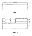
- FIG. 1 shows a cross-sectional view of a semiconductor substrate with a shallow trench isolation region according to the prior art.
- Substrate 10 includes a STI having a trench with corner implants 13 and sidewall implants 14.
- One conventional method for fabricating corner implants 13 requires the formation and patterning of photoresist mask 12 on the device and the implantation of dopants (represented by arrows) into the corners of the shallow trench.
- dopants represented by arrows
- corner implants 13 Another method to form corner implants 13 is to remove a hard mask (not shown) from the sidewalls and corners of the shallow trench region of the semiconductor substrate and then simultaneously implant both the sidewalls and corners. Unfortunately, subsequent etches performed during the fabrication process can create undesirable silicon pits at the corner implants of the STI.
- the present invention is directed to overcoming one or more of the problems set forth above.
- the present invention relates to a method for fabricating an image sensor with corner implants in the shallow trench isolation regions.
- the method includes the steps of forming a first hard mask layer of over an etch-stop layer on a semiconductor substrate and providing a photoresist mask over the hard mask layer.
- the photoresist mask is patterned to create an opening and the portion of the first hard mask layer exposed in the opening is etched down to the etch-stop layer.
- a first dopant is then implanted into the semiconductor substrate through the exposed etch-stop layer.
- the photoresist mask is removed and a second hard mask layer is formed on the remaining structure and etched to create sidewall spacers along the side edges of the first hard mask layer.
- the etch stop layer and the semiconductor substrate positioned between the sidewall spacers are then etched to create a trench and a second dopant implanted into the side and bottom walls of the trench.
- the trench is then typically filled with a dielectric material to create a shallow trench isolation region in the semiconductor substrate.
- the present advantage has the advantage of reducing the surface dark current by forming corner implants that do not cause silicon pitting with a shallow trench isolation that is self-aligned.
- the present invention includes a method for forming corner implants in STI regions of an integrated circuit.
- the implant is self-aligned to the STI corner without the need for additional photoresist masking or exposing the STI corner, which can lead to silicon pitting.
- the present invention is described with reference to the accompanying drawings, in which exemplary embodiments of the invention are shown. The invention may, however, be embodied in may different forms and should not be construed as being limited to the embodiments set forth herein; rather, these embodiments are provided to fully convey the concept of the present invention to those skilled in the art.
- the drawings are not to scale and many portions are exaggerated for clarity.
- Semiconductor substrate 20 is silicon, silicon carbide, silicon-on-insulator, silicon-germanium, gallium-nitride, or gallium-arsenide in one embodiment in accordance with the invention. Furthermore, semiconductor substrate 20 can be n-type, p-type or an undoped substrate. Additionally, semiconductor substrate 20 may optionally have an epitaxial layer (not shown) that is the same or opposite conductivity type as semiconductor substrate 20. Semiconductor substrate 20 may also contain wells that are of the same or opposite conductivity type as either the epitaxial layer or semiconductor substrate 20 implanted therein.
- Etch-stop layer 21 is formed on the surface of semiconductor substrate 20.
- etch-stop layer 21 is formed as a thin layer of silicon dioxide or polysilicon.
- a silicon dioxide etch-stop layer may be grown on the substrate in oxygen or steam typically at 800 - 1200°C.
- etch stop layer 21 may be deposited directly on the surface of semiconductor substrate 20 by oxide chemical vapor deposition. Oxide chemical vapor deposition is accomplished by a low-pressure low temperature deposition or a plasma enhanced chemical vapor deposition.
- First hard mask layer 22 is deposited on etch-stop layer 21 via traditional processes such as low pressure chemical vapor deposition (LPCVD) or plasma enhanced chemical vapor deposition (PECVD).
- First hard mask layer 22 is configured as any mask layer that is deposited or grown on the device. Examples of a hard mask layer include, but are not limited to, silicon nitride, polysilicon and a metal film.
- FIG. 3 shows a cross-sectional view of a semiconductor substrate with an etched first hard mask layer in an embodiment in accordance with the invention.
- Photoresist mask 23 is coated onto first hard mask layer 22 and patterned to form opening 18.
- An anisotropic etch is then performed to remove the portion of first hard mask layer 22 exposed in opening 18.
- Opening 19 in first hard mask layer 22 is wider than the width of a shallow trench that will be formed in semiconductor substrate 20.
- Shallow implant 24 is typically implanted to a depth between 100 and 500A in an embodiment in accordance with the invention.
- Photoresist mask 23 and first hard mask layer 22 serve as a protective mask for the regions of the semiconductor substrate in which a shallow implant is not to be formed.
- Shallow implant 24 is a dopant having a conductivity type opposite the conductivity type of the photodetectors (not shown) in the image sensor.
- the dopant is an n-type dopant such as phosphorus, arsenic, or antimony.
- the dopant is a p-type dopant such as boron, aluminum, gallium or indium.
- the implant energy depends on the particular dopant used and is typically between 5-200KeV for an implant depth typically between 100 and 500A.
- the implant profile distribution is such that the implant dopant remains near the surface of substrate 20. If thermal processing occurs after implantation the dopant will diffuse away from the initial implant area. This diffusion is accounted for when choosing the initial implant depth and concentration of the elementary dopant.
- Photoresist mask 23 is then removed by an oxygen ashing process, wet sulfuric acid mixed with peroxide, or solvent chemistry methods. If adequate thickness is used for first hard mask layer 22, photoresist mask 23 is removed and first hard mask layer 22 is the protective mask for the implant in an embodiment in accordance with the invention. In another embodiment in accordance with the invention, shallow implant 24 is formed in substrate 20 before first hard mask layer 22 is ansiotropically etched.
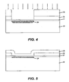
- FIG. 5 shows a cross-sectional view of a semiconductor substrate with a second hard mask layer in an embodiment in accordance with the invention.
- Second hard mask layer 25 is deposited on first hard mask layer 22 and the exposed portion of etch-stop layer 21.
- Second hard mask layer 25 may be of the same or different material than first hard mask layer 22.
- Second hard mask layer 25 is of a material that has a slow removal rate during an STI anisotropic etch when compared to the silicon removal rate in an embodiment in accordance with the invention.
- FIG. 6 a cross-sectional view of a semiconductor substrate with an etched second hard mask layer in an embodiment in accordance with the invention is shown.
- An anisotropic etch such as plasma etching, is used to form sidewall spacers 26 along the sides of first hard mask layer 22.
- Sidewall spacers 26 are positioned over the perimeter portions of shallow implant 24.
- Sidewall spacers 26 each typically have a width between 0.05 and 0.2 ⁇ m in an embodiment in accordance with the invention. The width of sidewall spacers 26 is primarily controlled by the thickness of second hard mask layer 25 (see FIG. 5 ).
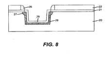
- FIG. 7 shows a cross-sectional view of a semiconductor substrate with a shallow trench in an embodiment in accordance with the invention.
- Shallow trench 40 is formed by anisotropically etching through shallow implant 24 and into semiconductor substrate 20.
- Shallow trench 40 is formed in the area between sidewall spacers 26 in semiconductor substrate 20.
- Corner implants 27 are the only portions of shallow implant 24 to remain in substrate 20. By etching through opening 19 in second hard mask layer 25, the inside edges of corner implants 27 are self-aligned with the inside edge of second hard mask layer 25.
- shallow trench 40 typically has a depth between 0.3 and 0.5 ⁇ m and a width between 0.15 and 0.6 ⁇ m.
- the width of shallow trench 40 should be as small as possible to minimize the amount of semiconductor substrate used for the STI regions. Minimizing the size of the STI regions advantageously increases the amount of substrate that is available for photodetectors in an image sensor.
- Implant dopant 28 is typically implanted between 0 and 100A from the exposed surface of the substrate 20 and the concentration of implant dopant 28 is typically between 10 12 -10 13 atoms/cm 2 in an embodiment in accordance with the invention.
- This implant is usually done at an angle and quaded (i.e., done at four separate wafer rotations ninety degrees apart) so that implant dopant 28 is implanted into all four sides and the bottom of shallow trench 40.
- Implant dopant 28 is of the same conductivity type as the corner implants 27. In one embodiment in accordance with the invention, implant dopant 28 is also the same dopant as the shallow implant 24 dopant. Implant dopant 28 can be an n-type dopant such as phosphorus, arsenic, or antimony, or a p-type dopant such as boron, aluminum, gallium or indium.
- Dielectric layer 29 is typically formed on the regions of the silicon implanted with dopant 28 by a low-pressure chemical vapor deposition, an atmospheric pressure chemical vapor deposition, a plasma enhanced chemical vapor deposition, or a high density plasma deposition.
- a dielectric material that can be used for dielectric layer 29 include, but are not limited to, a liner oxide or nitride.
- Dielectric layer 29 can be grown or deposited either prior to or after the implantation of implant dopant 28. Isolation trench 40 is then filled with a dielectric material (not shown).
- FIG. 9a a first cross-sectional view of a semiconductor substrate containing devices between two shallow trench isolations with sidewall implants in embodiments in accordance with the invention is shown.
- STI regions 42, 43 are shown adjacent to photodetectors 30, 31, respectively.
- Photodetectors 30, 31 have a conductivity type that is opposite the conductivity type of implant dopant 28 and corner implants 27.
- transfer gate 32 is pulsed, charge is transferred from one photodetector (e.g., photodetector 30 ) into floating diffusion 33, also referred to as a sensing node, contained in well 34.
- the signal is then sensed by the pixel amplifier (not shown) and fed into the downstream circuitry (not shown) outside of the pixel array.
- Floating diffusion 33 has a conductivity type that is opposite the conductivity type of implant dopant 28 and corner implants 27.
- FIG. 9b shows a second cross-sectional view of a semiconductor substrate containing devices between two shallow trench isolations with sidewall implants in embodiments in accordance with the invention.
- the conductivity type of corner implants 27, implant dopant 28, photodetectors 30, 31, floating diffusion 33, well 34, and pining layers 35, 36 is reversed with respect to the conductivity types shown in FIG. 9a .
- the first hard mask layer and second hard mask layer have been removed from the structure shown in FIGS. 9a and 9b . However, it is understood that these layers may alternatively remain in the final structure.
- an image sensor with two shared photodetectors is shown in FIGS. 9a and 9b it is understood that any number of photodetectors may be used. Typically one, two or four photodetectors can be connected to a single floating diffusion by transfer gates. The photodetectors are usually formed at a depth that is less than the shallow trench.
Claims (7)
- Procédé pour former une zone isolante dans un substrat semi-conducteur afin d'isoler les dispositifs formés dans le substrat, comprenant dans l'ordre les étapes suivantes :a) formation d'un implant peu profond (24) dans une portion du substrat semi-conducteur (20) en implantant un premier dopant à travers une ouverture (19) dans un premier masque dur (22) ;b) formation d'un deuxième masque dur (25) au-dessus de la portion du substrat semi-conducteur (20) et du premier masque dur (22) ;c) gravure du deuxième masque dur (25) pour former des éléments d'espacement latéraux (26) le long des bords du premier masque dur (22), où chaque élément d'espacement latéral (26) recouvre une portion de l'implant peu profond (24) dans le substrat semi-conducteur (20) ; etd) gravure dans le substrat semi-conducteur (20) entre les éléments d'espacement latéraux (26) pour former une tranchée isolante (40) et des implants d'angle (27).
- Procédé selon la revendication 1, comprenant aussi :la formation d'une couche d'arrêt de gravure (21) au-dessus de la surface du substrat semi-conducteur ;la formation du premier masque dur (22) au-dessus de la couche d'arrêt de gravure (21) ;l'application d'un masque de photoresist (23) au-dessus du premier masque dur (22) ;le modelage du masque de photoresist (23) pour former une ouverture (18) dans le masque de photoresist (23) ; etla gravure du premier masque dur (22) à travers l'ouverture (18) dans le masque de photoresist (23) pour former l'ouverture (19) dans le premier masque dur (22).
- Procédé selon la revendication 1, comprenant aussi :l'implantation d'un deuxième dopant (28) dans les parois latérales et le fond de la tranchée isolante (40).
- Procédé selon la revendication 3, comprenant aussi la formation d'une couche isolante conforme (29) au-dessus des parois latérales et du fond de la tranchée isolante (40).
- Procédé selon la revendication 3, dans lequel le deuxième dopant (28) a le même type de conductivité que le premier dopant.
- Procédé selon la revendication 2, comprenant aussi l'étape de formation d'un photodétecteur (30, 31) dans le substrat semi-conducteur (20) pour capturer la lumière et la convertir en une charge, dans lequel le photodétecteur (30, 31) est latéralement adjacent à la tranchée isolante (40).
- Procédé selon la revendication 2, dans lequel l'étape de gravure du substrat semi-conducteur (20) entre les éléments d'espacement latéraux (26) pour former une tranchée isolante (40) et des implants d'angle (27) aligne automatiquement un bord intérieur de chaque implant d'angle (27) avec un bord intérieur d'un élément d'espacement latéral correspondant (26).
Applications Claiming Priority (3)
| Application Number | Priority Date | Filing Date | Title |
|---|---|---|---|
| US84207506P | 2006-09-01 | 2006-09-01 | |
| US11/840,299 US20080057612A1 (en) | 2006-09-01 | 2007-08-17 | Method for adding an implant at the shallow trench isolation corner in a semiconductor substrate |
| PCT/US2007/018997 WO2008030371A2 (fr) | 2006-09-01 | 2007-08-29 | Implant au niveau d'un angle d'isolation par tranchée peu profonde |
Publications (2)
| Publication Number | Publication Date |
|---|---|
| EP2057675A2 EP2057675A2 (fr) | 2009-05-13 |
| EP2057675B1 true EP2057675B1 (fr) | 2010-09-29 |
Family
ID=39031210
Family Applications (1)
| Application Number | Title | Priority Date | Filing Date |
|---|---|---|---|
| EP07837483A Active EP2057675B1 (fr) | 2006-09-01 | 2007-08-29 | Implant au niveau d'un angle d'isolation par tranchée peu profonde |
Country Status (7)
| Country | Link |
|---|---|
| US (1) | US20080057612A1 (fr) |
| EP (1) | EP2057675B1 (fr) |
| JP (1) | JP5281008B2 (fr) |
| KR (1) | KR101329462B1 (fr) |
| DE (1) | DE602007009548D1 (fr) |
| TW (1) | TWI413167B (fr) |
| WO (1) | WO2008030371A2 (fr) |
Cited By (1)
| Publication number | Priority date | Publication date | Assignee | Title |
|---|---|---|---|---|
| TWI587490B (zh) * | 2012-06-08 | 2017-06-11 | 台灣積體電路製造股份有限公司 | 影像感測元件與其形成方法 |
Families Citing this family (19)
| Publication number | Priority date | Publication date | Assignee | Title |
|---|---|---|---|---|
| US20100148230A1 (en) * | 2008-12-11 | 2010-06-17 | Stevens Eric G | Trench isolation regions in image sensors |
| US7968424B2 (en) * | 2009-01-16 | 2011-06-28 | Taiwan Semiconductor Manufacturing Company, Ltd. | Method of implantation |
| US7838325B2 (en) * | 2009-02-13 | 2010-11-23 | Taiwan Semiconductor Manufacturing Company, Ltd. | Method to optimize substrate thickness for image sensor device |
| US9196547B2 (en) | 2009-04-03 | 2015-11-24 | Taiwan Semiconductor Manufacturing Company, Ltd. | Dual shallow trench isolation and related applications |
| US8048711B2 (en) * | 2009-12-30 | 2011-11-01 | Omnivision Technologies, Inc. | Method for forming deep isolation in imagers |
| US9000500B2 (en) | 2009-12-30 | 2015-04-07 | Omnivision Technologies, Inc. | Image sensor with doped transfer gate |
| US8367512B2 (en) | 2010-08-30 | 2013-02-05 | Taiwan Semiconductor Manufacturing Company, Ltd. | Self-aligned implants to reduce cross-talk of imaging sensors |
| FR2981502A1 (fr) * | 2011-10-18 | 2013-04-19 | St Microelectronics Crolles 2 | Procede de realisation d'au moins une tranchee d'isolation profonde |
| US9673245B2 (en) | 2012-10-01 | 2017-06-06 | Taiwan Semiconductor Manufacturing Company, Ltd. | Implant isolated devices and method for forming the same |
| US9355888B2 (en) | 2012-10-01 | 2016-05-31 | Taiwan Semiconductor Manufacturing Company, Ltd. | Implant isolated devices and method for forming the same |
| US8969997B2 (en) * | 2012-11-14 | 2015-03-03 | Taiwan Semiconductor Manufacturing Company, Ltd. | Isolation structures and methods of forming the same |
| WO2014209421A1 (fr) * | 2013-06-29 | 2014-12-31 | Sionyx, Inc. | Régions texturées formées de tranchées peu profondes et procédés associés. |
| JP6362449B2 (ja) | 2014-07-01 | 2018-07-25 | ルネサスエレクトロニクス株式会社 | 半導体集積回路装置の製造方法 |
| KR102399338B1 (ko) * | 2014-09-12 | 2022-05-19 | 삼성전자주식회사 | 이미지 센서의 제조 방법 |
| US9647022B2 (en) * | 2015-02-12 | 2017-05-09 | Taiwan Semiconductor Manufacturing Co., Ltd. | Multi-layer structure for high aspect ratio etch |
| US10580789B2 (en) * | 2017-07-10 | 2020-03-03 | Macronix International Co., Ltd. | Semiconductor device having etching control layer in substrate and method of fabricating the same |
| CN109256389B (zh) * | 2017-07-13 | 2021-06-11 | 旺宏电子股份有限公司 | 半导体元件及其制造方法 |
| CN110021559B (zh) * | 2018-01-09 | 2021-08-24 | 联华电子股份有限公司 | 半导体元件及其制作方法 |
| US11923205B2 (en) * | 2021-12-17 | 2024-03-05 | United Microelectronics Corporation | Method for manufacturing semiconductor device |
Family Cites Families (27)
| Publication number | Priority date | Publication date | Assignee | Title |
|---|---|---|---|---|
| JPS6052580B2 (ja) * | 1978-10-20 | 1985-11-20 | 三洋電機株式会社 | 半導体装置に於ける表面保護膜の製法 |
| JPH01125935A (ja) * | 1987-11-11 | 1989-05-18 | Seiko Instr & Electron Ltd | 半導体装置の製造方法 |
| JPH0621047A (ja) * | 1992-05-08 | 1994-01-28 | Sanyo Electric Co Ltd | 半導体装置及びその製造方法 |
| US5780353A (en) * | 1996-03-28 | 1998-07-14 | Advanced Micro Devices, Inc. | Method of doping trench sidewalls before trench etching |
| US5874346A (en) * | 1996-05-23 | 1999-02-23 | Advanced Micro Devices, Inc. | Subtrench conductor formation with large tilt angle implant |
| US5891787A (en) * | 1997-09-04 | 1999-04-06 | Advanced Micro Devices, Inc. | Semiconductor fabrication employing implantation of excess atoms at the edges of a trench isolation structure |
| US6030898A (en) * | 1997-12-19 | 2000-02-29 | Advanced Micro Devices, Inc. | Advanced etching method for VLSI fabrication |
| US6096612A (en) * | 1998-04-30 | 2000-08-01 | Texas Instruments Incorporated | Increased effective transistor width using double sidewall spacers |
| KR100372103B1 (ko) * | 1998-06-30 | 2003-03-31 | 주식회사 하이닉스반도체 | 반도체소자의소자분리방법 |
| TW391051B (en) * | 1998-11-06 | 2000-05-21 | United Microelectronics Corp | Method for manufacturing shallow trench isolation structure |
| TW406350B (en) * | 1998-12-07 | 2000-09-21 | United Microelectronics Corp | Method for manufacturing the shallow trench isolation area |
| TW486774B (en) * | 1998-12-19 | 2002-05-11 | United Microelectronics Corp | Shallow trench isolation technique joining field oxide layer |
| JP3425896B2 (ja) * | 1999-06-15 | 2003-07-14 | Necエレクトロニクス株式会社 | 半導体装置の製造方法 |
| KR20010059185A (ko) * | 1999-12-30 | 2001-07-06 | 박종섭 | 반도체소자의 소자분리막 형성방법 |
| US6150235A (en) * | 2000-01-24 | 2000-11-21 | Worldwide Semiconductor Manufacturing Corp. | Method of forming shallow trench isolation structures |
| US6437417B1 (en) * | 2000-08-16 | 2002-08-20 | Micron Technology, Inc. | Method for making shallow trenches for isolation |
| US6624016B2 (en) * | 2001-02-22 | 2003-09-23 | Silicon-Based Technology Corporation | Method of fabricating trench isolation structures with extended buffer spacers |
| KR100438403B1 (ko) * | 2001-09-05 | 2004-07-02 | 동부전자 주식회사 | 플랫 셀 메모리 소자의 제조방법 |
| JP4087108B2 (ja) * | 2001-12-10 | 2008-05-21 | シャープ株式会社 | 不揮発性半導体記憶装置及びその製造方法 |
| KR100480897B1 (ko) * | 2002-12-09 | 2005-04-07 | 매그나칩 반도체 유한회사 | 반도체소자의 소자분리막 형성방법 |
| US7102184B2 (en) * | 2003-06-16 | 2006-09-05 | Micron Technology, Inc. | Image device and photodiode structure |
| US7067387B2 (en) * | 2003-08-28 | 2006-06-27 | Taiwan Semiconductor Manufacturing Company | Method of manufacturing dielectric isolated silicon structure |
| US6951780B1 (en) * | 2003-12-18 | 2005-10-04 | Matrix Semiconductor, Inc. | Selective oxidation of silicon in diode, TFT, and monolithic three dimensional memory arrays |
| US7154136B2 (en) * | 2004-02-20 | 2006-12-26 | Micron Technology, Inc. | Isolation structures for preventing photons and carriers from reaching active areas and methods of formation |
| US7045410B2 (en) * | 2004-07-27 | 2006-05-16 | Texas Instruments Incorporated | Method to design for or modulate the CMOS transistor threshold voltage using shallow trench isolation (STI) |
| US7279397B2 (en) * | 2004-07-27 | 2007-10-09 | Texas Instruments Incorporated | Shallow trench isolation method |
| US7262110B2 (en) * | 2004-08-23 | 2007-08-28 | Micron Technology, Inc. | Trench isolation structure and method of formation |
-
2007
- 2007-08-17 US US11/840,299 patent/US20080057612A1/en not_active Abandoned
- 2007-08-29 WO PCT/US2007/018997 patent/WO2008030371A2/fr active Application Filing
- 2007-08-29 DE DE602007009548T patent/DE602007009548D1/de active Active
- 2007-08-29 KR KR1020097004162A patent/KR101329462B1/ko active IP Right Grant
- 2007-08-29 JP JP2009526696A patent/JP5281008B2/ja active Active
- 2007-08-29 EP EP07837483A patent/EP2057675B1/fr active Active
- 2007-08-31 TW TW096132663A patent/TWI413167B/zh active
Cited By (1)
| Publication number | Priority date | Publication date | Assignee | Title |
|---|---|---|---|---|
| TWI587490B (zh) * | 2012-06-08 | 2017-06-11 | 台灣積體電路製造股份有限公司 | 影像感測元件與其形成方法 |
Also Published As
| Publication number | Publication date |
|---|---|
| TW200830381A (en) | 2008-07-16 |
| JP2010503212A (ja) | 2010-01-28 |
| WO2008030371A3 (fr) | 2008-04-17 |
| JP5281008B2 (ja) | 2013-09-04 |
| US20080057612A1 (en) | 2008-03-06 |
| EP2057675A2 (fr) | 2009-05-13 |
| KR101329462B1 (ko) | 2013-11-13 |
| DE602007009548D1 (de) | 2010-11-11 |
| KR20090045294A (ko) | 2009-05-07 |
| WO2008030371A2 (fr) | 2008-03-13 |
| TWI413167B (zh) | 2013-10-21 |
Similar Documents
| Publication | Publication Date | Title |
|---|---|---|
| EP2057675B1 (fr) | Implant au niveau d'un angle d'isolation par tranchée peu profonde | |
| US7491561B2 (en) | Pixel sensor having doped isolation structure sidewall | |
| EP1213757B1 (fr) | Circuits intégrés et régions adjacentes p-dopées avec des structures d'isolation par tranchées peu profondes sans revêtement du type "Liner" et méthodes de fabrication | |
| KR100748342B1 (ko) | 씨모스 이미지 센서의 제조방법 | |
| US20060276014A1 (en) | Self-aligned high-energy implantation for deep junction structure | |
| US7732246B2 (en) | Method for fabricating vertical CMOS image sensor | |
| US7528427B2 (en) | Pixel sensor cell having asymmetric transfer gate with reduced pinning layer barrier potential | |
| EP2323161A2 (fr) | Structure d'isolation de tranches peu profondes présentant un entrefer, capteur d'images cmos utilisant une telle structure et procédé de production correspondant | |
| CN109728010B (zh) | 集成芯片及其形成方法 | |
| JP2005197682A (ja) | Cmosイメージセンサ及びその製造方法 | |
| JP2007027686A (ja) | イメージセンサ及びその製造方法 | |
| TWI458045B (zh) | 製備自我對準隔離區的方法 | |
| US11705475B2 (en) | Method of forming shallow trench isolation (STI) structure for suppressing dark current | |
| US7429496B2 (en) | Buried photodiode for image sensor with shallow trench isolation technology | |
| US8987033B2 (en) | Method for forming CMOS image sensors | |
| JP2007300084A (ja) | プラズマ損傷からフォトダイオードを保護するcmosイメージセンサの製造方法 | |
| CN116110920A (zh) | 半导体结构的制造方法及半导体结构 | |
| CN101512752A (zh) | 在浅沟槽隔离拐角处的注入 | |
| KR100518868B1 (ko) | 이미지센서 및 그 제조방법 | |
| US20080299700A1 (en) | Method for fabricating photodiode | |
| KR20070096555A (ko) | 소자 분리 영역 형성 방법 및 이를 이용한 이미지 소자형성 방법 |
Legal Events
| Date | Code | Title | Description |
|---|---|---|---|
| PUAI | Public reference made under article 153(3) epc to a published international application that has entered the european phase |
Free format text: ORIGINAL CODE: 0009012 |
|
| 17P | Request for examination filed |
Effective date: 20090302 |
|
| AK | Designated contracting states |
Kind code of ref document: A2 Designated state(s): AT BE BG CH CY CZ DE DK EE ES FI FR GB GR HU IE IS IT LI LT LU LV MC MT NL PL PT RO SE SI SK TR |
|
| AX | Request for extension of the european patent |
Extension state: AL BA HR MK RS |
|
| RIN1 | Information on inventor provided before grant (corrected) |
Inventor name: STEVENS, ERIC, GORDON Inventor name: DOAN, HUNG, QUOC |
|
| 17Q | First examination report despatched |
Effective date: 20090810 |
|
| DAX | Request for extension of the european patent (deleted) | ||
| GRAP | Despatch of communication of intention to grant a patent |
Free format text: ORIGINAL CODE: EPIDOSNIGR1 |
|
| GRAS | Grant fee paid |
Free format text: ORIGINAL CODE: EPIDOSNIGR3 |
|
| GRAA | (expected) grant |
Free format text: ORIGINAL CODE: 0009210 |
|
| RBV | Designated contracting states (corrected) |
Designated state(s): DE FR GB NL |
|
| AK | Designated contracting states |
Kind code of ref document: B1 Designated state(s): DE FR GB NL |
|
| REG | Reference to a national code |
Ref country code: GB Ref legal event code: FG4D |
|
| REF | Corresponds to: |
Ref document number: 602007009548 Country of ref document: DE Date of ref document: 20101111 Kind code of ref document: P |
|
| REG | Reference to a national code |
Ref country code: NL Ref legal event code: T3 |
|
| REG | Reference to a national code |
Ref country code: GB Ref legal event code: 732E Free format text: REGISTERED BETWEEN 20110704 AND 20110706 |
|
| PLBE | No opposition filed within time limit |
Free format text: ORIGINAL CODE: 0009261 |
|
| STAA | Information on the status of an ep patent application or granted ep patent |
Free format text: STATUS: NO OPPOSITION FILED WITHIN TIME LIMIT |
|
| REG | Reference to a national code |
Ref country code: NL Ref legal event code: SD Effective date: 20110815 |
|
| REG | Reference to a national code |
Ref country code: DE Ref legal event code: R082 Ref document number: 602007009548 Country of ref document: DE Representative=s name: WAGNER & GEYER PARTNERSCHAFT MBB PATENT- UND R, DE Effective date: 20110729 Ref country code: DE Ref legal event code: R082 Ref document number: 602007009548 Country of ref document: DE Representative=s name: WAGNER & GEYER PARTNERSCHAFT PATENT- UND RECHT, DE Effective date: 20110729 Ref country code: DE Ref legal event code: R081 Ref document number: 602007009548 Country of ref document: DE Owner name: OMNIVISION TECHNOLOGIES, INC., SANTA CLARA, US Free format text: FORMER OWNER: EASTMAN KODAK CO., ROCHESTER, N.Y., US Effective date: 20110729 |
|
| REG | Reference to a national code |
Ref country code: DE Ref legal event code: R097 Ref document number: 602007009548 Country of ref document: DE Effective date: 20110630 |
|
| REG | Reference to a national code |
Ref country code: FR Ref legal event code: PLFP Year of fee payment: 10 |
|
| REG | Reference to a national code |
Ref country code: FR Ref legal event code: PLFP Year of fee payment: 11 |
|
| REG | Reference to a national code |
Ref country code: FR Ref legal event code: PLFP Year of fee payment: 12 |
|
| PGFP | Annual fee paid to national office [announced via postgrant information from national office to epo] |
Ref country code: NL Payment date: 20230720 Year of fee payment: 17 |
|
| PGFP | Annual fee paid to national office [announced via postgrant information from national office to epo] |
Ref country code: GB Payment date: 20230712 Year of fee payment: 17 |
|
| PGFP | Annual fee paid to national office [announced via postgrant information from national office to epo] |
Ref country code: FR Payment date: 20230710 Year of fee payment: 17 Ref country code: DE Payment date: 20230711 Year of fee payment: 17 |