EP2042913A2 - Modulateur optique de phase par déplacement de phase en quadrature - Google Patents
Modulateur optique de phase par déplacement de phase en quadrature Download PDFInfo
- Publication number
- EP2042913A2 EP2042913A2 EP08013952A EP08013952A EP2042913A2 EP 2042913 A2 EP2042913 A2 EP 2042913A2 EP 08013952 A EP08013952 A EP 08013952A EP 08013952 A EP08013952 A EP 08013952A EP 2042913 A2 EP2042913 A2 EP 2042913A2
- Authority
- EP
- European Patent Office
- Prior art keywords
- light
- phase
- outputted
- light source
- outputs
- Prior art date
- Legal status (The legal status is an assumption and is not a legal conclusion. Google has not performed a legal analysis and makes no representation as to the accuracy of the status listed.)
- Withdrawn
Links
Images


Classifications
-
- G—PHYSICS
- G02—OPTICS
- G02F—OPTICAL DEVICES OR ARRANGEMENTS FOR THE CONTROL OF LIGHT BY MODIFICATION OF THE OPTICAL PROPERTIES OF THE MEDIA OF THE ELEMENTS INVOLVED THEREIN; NON-LINEAR OPTICS; FREQUENCY-CHANGING OF LIGHT; OPTICAL LOGIC ELEMENTS; OPTICAL ANALOGUE/DIGITAL CONVERTERS
- G02F1/00—Devices or arrangements for the control of the intensity, colour, phase, polarisation or direction of light arriving from an independent light source, e.g. switching, gating or modulating; Non-linear optics
- G02F1/01—Devices or arrangements for the control of the intensity, colour, phase, polarisation or direction of light arriving from an independent light source, e.g. switching, gating or modulating; Non-linear optics for the control of the intensity, phase, polarisation or colour
- G02F1/0121—Operation of devices; Circuit arrangements, not otherwise provided for in this subclass
- G02F1/0123—Circuits for the control or stabilisation of the bias voltage, e.g. automatic bias control [ABC] feedback loops
-
- G—PHYSICS
- G02—OPTICS
- G02F—OPTICAL DEVICES OR ARRANGEMENTS FOR THE CONTROL OF LIGHT BY MODIFICATION OF THE OPTICAL PROPERTIES OF THE MEDIA OF THE ELEMENTS INVOLVED THEREIN; NON-LINEAR OPTICS; FREQUENCY-CHANGING OF LIGHT; OPTICAL LOGIC ELEMENTS; OPTICAL ANALOGUE/DIGITAL CONVERTERS
- G02F1/00—Devices or arrangements for the control of the intensity, colour, phase, polarisation or direction of light arriving from an independent light source, e.g. switching, gating or modulating; Non-linear optics
- G02F1/01—Devices or arrangements for the control of the intensity, colour, phase, polarisation or direction of light arriving from an independent light source, e.g. switching, gating or modulating; Non-linear optics for the control of the intensity, phase, polarisation or colour
- G02F1/21—Devices or arrangements for the control of the intensity, colour, phase, polarisation or direction of light arriving from an independent light source, e.g. switching, gating or modulating; Non-linear optics for the control of the intensity, phase, polarisation or colour by interference
- G02F1/225—Devices or arrangements for the control of the intensity, colour, phase, polarisation or direction of light arriving from an independent light source, e.g. switching, gating or modulating; Non-linear optics for the control of the intensity, phase, polarisation or colour by interference in an optical waveguide structure
- G02F1/2255—Devices or arrangements for the control of the intensity, colour, phase, polarisation or direction of light arriving from an independent light source, e.g. switching, gating or modulating; Non-linear optics for the control of the intensity, phase, polarisation or colour by interference in an optical waveguide structure controlled by a high-frequency electromagnetic component in an electric waveguide structure
-
- H—ELECTRICITY
- H04—ELECTRIC COMMUNICATION TECHNIQUE
- H04B—TRANSMISSION
- H04B10/00—Transmission systems employing electromagnetic waves other than radio-waves, e.g. infrared, visible or ultraviolet light, or employing corpuscular radiation, e.g. quantum communication
- H04B10/50—Transmitters
- H04B10/501—Structural aspects
- H04B10/503—Laser transmitters
- H04B10/505—Laser transmitters using external modulation
- H04B10/5053—Laser transmitters using external modulation using a parallel, i.e. shunt, combination of modulators
-
- H—ELECTRICITY
- H04—ELECTRIC COMMUNICATION TECHNIQUE
- H04B—TRANSMISSION
- H04B10/00—Transmission systems employing electromagnetic waves other than radio-waves, e.g. infrared, visible or ultraviolet light, or employing corpuscular radiation, e.g. quantum communication
- H04B10/50—Transmitters
- H04B10/501—Structural aspects
- H04B10/503—Laser transmitters
- H04B10/505—Laser transmitters using external modulation
- H04B10/5057—Laser transmitters using external modulation using a feedback signal generated by analysing the optical output
- H04B10/50577—Laser transmitters using external modulation using a feedback signal generated by analysing the optical output to control the phase of the modulating signal
-
- H—ELECTRICITY
- H04—ELECTRIC COMMUNICATION TECHNIQUE
- H04B—TRANSMISSION
- H04B10/00—Transmission systems employing electromagnetic waves other than radio-waves, e.g. infrared, visible or ultraviolet light, or employing corpuscular radiation, e.g. quantum communication
- H04B10/50—Transmitters
- H04B10/501—Structural aspects
- H04B10/503—Laser transmitters
- H04B10/505—Laser transmitters using external modulation
- H04B10/5059—Laser transmitters using external modulation using a feed-forward signal generated by analysing the optical or electrical input
- H04B10/50595—Laser transmitters using external modulation using a feed-forward signal generated by analysing the optical or electrical input to control the modulator DC bias
-
- H—ELECTRICITY
- H04—ELECTRIC COMMUNICATION TECHNIQUE
- H04L—TRANSMISSION OF DIGITAL INFORMATION, e.g. TELEGRAPHIC COMMUNICATION
- H04L27/00—Modulated-carrier systems
- H04L27/18—Phase-modulated carrier systems, i.e. using phase-shift keying
- H04L27/20—Modulator circuits; Transmitter circuits
- H04L27/2032—Modulator circuits; Transmitter circuits for discrete phase modulation, e.g. in which the phase of the carrier is modulated in a nominally instantaneous manner
- H04L27/2053—Modulator circuits; Transmitter circuits for discrete phase modulation, e.g. in which the phase of the carrier is modulated in a nominally instantaneous manner using more than one carrier, e.g. carriers with different phases
- H04L27/206—Modulator circuits; Transmitter circuits for discrete phase modulation, e.g. in which the phase of the carrier is modulated in a nominally instantaneous manner using more than one carrier, e.g. carriers with different phases using a pair of orthogonal carriers, e.g. quadrature carriers
- H04L27/2067—Modulator circuits; Transmitter circuits for discrete phase modulation, e.g. in which the phase of the carrier is modulated in a nominally instantaneous manner using more than one carrier, e.g. carriers with different phases using a pair of orthogonal carriers, e.g. quadrature carriers with more than two phase states
- H04L27/2071—Modulator circuits; Transmitter circuits for discrete phase modulation, e.g. in which the phase of the carrier is modulated in a nominally instantaneous manner using more than one carrier, e.g. carriers with different phases using a pair of orthogonal carriers, e.g. quadrature carriers with more than two phase states in which the data are represented by the carrier phase, e.g. systems with differential coding
-
- H—ELECTRICITY
- H04—ELECTRIC COMMUNICATION TECHNIQUE
- H04L—TRANSMISSION OF DIGITAL INFORMATION, e.g. TELEGRAPHIC COMMUNICATION
- H04L27/00—Modulated-carrier systems
- H04L27/18—Phase-modulated carrier systems, i.e. using phase-shift keying
- H04L27/20—Modulator circuits; Transmitter circuits
- H04L27/2096—Arrangements for directly or externally modulating an optical carrier
-
- G—PHYSICS
- G02—OPTICS
- G02F—OPTICAL DEVICES OR ARRANGEMENTS FOR THE CONTROL OF LIGHT BY MODIFICATION OF THE OPTICAL PROPERTIES OF THE MEDIA OF THE ELEMENTS INVOLVED THEREIN; NON-LINEAR OPTICS; FREQUENCY-CHANGING OF LIGHT; OPTICAL LOGIC ELEMENTS; OPTICAL ANALOGUE/DIGITAL CONVERTERS
- G02F1/00—Devices or arrangements for the control of the intensity, colour, phase, polarisation or direction of light arriving from an independent light source, e.g. switching, gating or modulating; Non-linear optics
- G02F1/01—Devices or arrangements for the control of the intensity, colour, phase, polarisation or direction of light arriving from an independent light source, e.g. switching, gating or modulating; Non-linear optics for the control of the intensity, phase, polarisation or colour
- G02F1/21—Devices or arrangements for the control of the intensity, colour, phase, polarisation or direction of light arriving from an independent light source, e.g. switching, gating or modulating; Non-linear optics for the control of the intensity, phase, polarisation or colour by interference
- G02F1/212—Mach-Zehnder type
Definitions
- the present invention relates to a technique for stabilizing control of a phase modulator, and in particular, to a quaternary phase modulator which modulates the phase of a light on four levels.
- Chromatic dispersion (hereafter, distribution) is the wavelength dependency of the group velocity with which a signal spreads in an optical fiber.
- a light waveform has plural wavelength components (i.e., spectral broadening), and if the group velocity has wavelength dependency, there will be a component which propagates slowly and a component which propagates rapidly in the optical fiber, and as a result, the waveform will broaden. Hence, if the amount of dispersion cannot be ignored, waveform distortion will occur and receiving characteristics will deteriorate.
- the transmission distance of a chromatic dispersion limit is in inverse proportion to the square of the transmission bandwidth. For example, if it is attempted to convert a signal propagating at 10Gbps to 40Gbps, the distance will be reduced to 1/16.
- the transmission distance at the polarization dispersion limit is in inverse proportion to the transmission bandwidth, and as in the previous example, if it is attempted to convert a signal propagating at 10Gbps to 40Gbps, the distance will be reduced to 1/4.
- the increase of bit rate also brings about an increase in signal bandwidth occupancy. For example, it is attempted to increase the bit rate by 4 times, the signal bandwidth occupancy, i.e., the spectral bandwidth of the occupying signal, is also increased by 4 times. If it is attempted to convert an optical signal to multi-channel in the wavelength direction such as in wavelength multiplexed transmission (WDM), the bandwidth is then limited by the amplification bandwidth of the optical amplifier which performs package amplification of this wavelength multiplexing signal. Specifically, if it is desired to set wavelengths so that wavelength multiplexing signals do not overlap, the product of the occupied spectral bandwidth and the wavelength number must necessarily be the amplification bandwidth of this optical amplifier.
- WDM wavelength multiplexed transmission
- the amplification bandwidth is constant and it is necessary to decrease the wavelength number if the occupied spectral bandwidth is increased, even if the bit rate is improved, the spectral bandwidth will increase by a corresponding amount and the wavelength number will decrease, so the total capacity does not change and conversion to high capacity will thus be limited.
- Optical multi-level modulation is now attracting attention as a way of overcoming the limitations of device response speed, the limitations due to chromatic dispersion and polarization, and the limitations due to broadening of spectral bandwidth.
- Optical multi-level modulation is a technique whereby, by performing M (M>2) modulations of light intensity, optical phase, or both, the total transmission capacity is increased by log M times (the base of the logarithm is 2), without increasing the bit rate of the modulation drive signal.
- the transmission capacity can be increased by 3 times by providing three signals of approximately 13Gbps.
- the transmission capacity can be increased by 4 times by providing four signals of 10Gbps. In both of these cases, therefore, 40Gbps transmission can be realized.
- the chromatic dispersion, polarization dispersion and occupied spectral bandwidth are limited by the rate of these driving signals, so in the case of a 40Gbps signal formed by two 20Gbps signals mentioned hereinabove, as compared to transmitting the 40GB/s signal by binary transmission according to the prior art, the chromatic dispersion limiting distance can be extended by 4 times, the polarization dispersion limiting distance can be extended by 2 times, and the occupied spectral bandwidth can be reduced to 1/2.
- QPSK Quadrature Phase Shift Keying
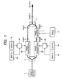
- FIG. 1 A signal light outputted from a light source (1) is split in a branching filter (2). The signal light split into two parts reaches phase modulators A and B (3A, 3B), respectively. An electrical signal wherein a bias voltage 1A (6A) is superposed on a data signal A (7A) by a bias superposer (8A), is applied to the phase modulator A. The lightwave signal inputted into the phase modulator A (3A) is subjected to binary phase modulation by this electrical signal, and the result is outputted.
- a bias voltage 1A (6A) is superposed on a data signal A (7A) by a bias superposer (8A
- a Mach-Zehnder (MZ) type interferometer is generally used for the phase modulator.
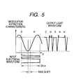
- the output characteristic (extinction characteristic) of the MZ modulator is shown in FIG. 2 .
- the applied voltage (horizontal axis) of the MZ modulator is varied, the output (vertical axis) from the modulator traces a locus which resembles a sinusoidal wave as shown in FIG. 2 .
- the voltage required for the extinction to change from a valley to a peak is a key parameter which is defined as V ⁇ , and represents the characteristic of the modulator.
- a binary electrical waveform of amplitude 2V ⁇ centered on the valley of the extinction characteristic (wherein the bias voltage is made to coincide with the valley of the extinction characteristic), is applied to this modulator. Since modulation is performed from peak to peak of the extinction characteristic, the output of the modulator is a waveform which first changes from a peak to a valley, and then becomes a peak again. Specifically, at the center of a bit, the output is always at the position of a peak and the amplitude is fixed. However, regarding the phase of the light, care is required. At adjacent peaks of the extinction characteristic of a MZ modulator, the phases of the outputted light differ by ⁇ .
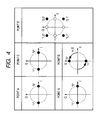
- FIG. 4 shows the phase states at a point A in FIG. 1 , i. e. , in the output of the phase modulator A (3A).
- the graphs of FIG. 4 are diagrams which represent the phase in a complex plane using the I-axis and the Q-axis.
- the I-axis represents the amount of an in-phase component
- the Q-axis represents the amount of a quadrature component.
- the distance of the signal point from the origin represents the amplitude of the signal.
- the angle between a line which connects the signal point from the origin, and a line which connects the positive direction of the I-axis from the origin represents the phase of the signal.
- two points are disposed on the I-axis symmetrically around the origin. Specifically, data signals of amplitudes "0", "1" are changed into two points of phase "0" and phase” ⁇ ", respectively.
- phase modulator B an electrical signal wherein a bias voltage 1B (6B) is superposed on a data signal B (7B) by a bias superposer (8B), is applied to the phase modulator B.
- the lightwave signal inputted into the phase modulator B (3B) is subjected to binary phase modulation by this electrical signal, and the result is outputted.
- a point B in FIG. 1 i.e., the phase state in the output of the phase modulator B (3B)
- data signals of amplitude "0", "1” are changed into two points of phase "0" and phase” ⁇ ", respectively.
- the phase adjuster (4) is installed in the output of the phase modulator B (3B), which is one of the two phase modulators.
- a bias voltage 2 is applied to the phase adjuster (4).
- the phase of the lightwave signal inputted into the phase adjuster (4) is adjusted by an amount according to this bias voltage 2, and is outputted.
- ⁇ /2 is an ideal value.
- the phase states at a point C and a point D give mutually different results, as shown in FIG. 4 . Specifically, the phase state at the point D, as a result of rotating each signal point by ⁇ /2, shifts to two points disposed on the Q-axis disposed symmetrically about the origin.
- the output of the phase modulator A (3A), and the output of the phase adjuster (4), are multiplexed by the multiplexer (5).
- the output of the multiplexer (5) i.e., the phase state of the signal points at a point E, is shown in FIG. 4 .
- These signal points correspond to four points shown by small circles with dotted lines in the diagram before multiplexing, and as a result of multiplexing by the multiplexer (5), four signal points are output which are a combined electric field, or geometrically, a combined vector, of these four points.
- x, y show the state of data A, and the state of data B, respectively, and the signal point when the data A is "0" and the data B is "1", i.e., "0, 1", is disposed at a point in the fourth quadrant of the coordinates.
- a quaternary phase modulation signal having the four phase levels + ⁇ /4, +3 ⁇ /4, -3 ⁇ /4 and - ⁇ /4, is formed.
- the quaternary phase modulation waveform as shown in FIG. 4 assumes that the bias voltage 1A (6A) of the phase modulator A (3A) and the bias voltage 1B (6B) of the phase modulator B (3B) both coincide with the valley of the extinction characteristic of the phase modulator, and that the bias voltage 2(9) of the phase adjuster (4) is equivalent to a phase shift of ⁇ /2.
- the case is considered where a bias drift occurs in the phase modulator A (3A), and the valley and bias voltage 1A (6A) of the phase modulator do not coincide.
- the center (bias) of the electrical waveform is offset from the valley of the extinction characteristic.
- the output reaches the peak of the extinction characteristic, but continues increasing even after reaching maximum output, and settles down to the middle of the peak. As a result, the amplitude of the output waveform will decrease.
- the result will be as shown in FIG. 6 .
- the modulator output i.e., the phase state at the point E, is characterized by a condensation in the I axis direction.
- the case is also considered when there is a bias drift in the phase adjuster (4), and the phase shift is less than ⁇ /2.
- the modulator output i.e., the phase state at the point E which was previously square, changes to a lozenge shape. Specifically, the amplitude in the states “1, 0", and “0, 1” will decrease, and the receiving sensitivity in the states “1, 0", “0, 1” will deteriorate.
- the ideal bias voltage at which the extinction characteristic of the phase modulators A, B is a valley, or the ideal bias voltage at which the phase shift of the phase adjuster (4) is ⁇ /2, is a different value for each device, so there was a problem that if a separate adjustment was not made for each device, it led to a deterioration of receiving sensitivity.
- phase modulator when the phase modulator was started up, it is necessary to perform control from the initial state (in many cases, zero voltage, or a certain default value memorized by the device) to an ideal bias voltage at which the extinction characteristic of the phase modulators A,B is a valley, or to perform control to the ideal bias voltage at which the phase shift of the phase adjuster (4) is ⁇ /2, and if such a control mechanism was not provided, there was a problem that this would also cause a deterioration of receiving sensitivity.
- a quaternary phase modulator includes: an optical branching filter which splits light output from a first light source into two parts; two phase modulators respectively disposed in the two outputs of the splitter, which respectively modulate the phases of the two lights, and output the resulting light; one phase adjuster disposed in one of the outputs of the phase modulators, which shifts the phase of the light and outputs the resulting light; an optical multiplexer which multiplexes the output light of the phase adjuster and the output light of the phase modulator on the side where the phase adjuster is not installed; and a second light source for a backward light which propagates in the opposite direction to that of the light output from the first light source in the quaternary phase modulator; and an optical coupler provided in the output of the optical multiplexer to introduce this second light source into the multi-level phase modulator, in which the quaternary phase modulator includes a first controller which feedback controls the bias voltage of the modulating electrical signal applied
- a quaternary phase modulator includes: an optical branching filter which splits light output from a first light source into two parts; two phase modulators respectively disposed in the two outputs of the modulators which respectively modulate the phases of the two lights, and output the resulting lights; one phase adjuster disposed in one of the outputs of the phase modulators, which shifts the phase of the light and outputs the resulting light; an optical .multiplexer which multiplexes the output light of the phase adjuster and the output light of the phase modulator on the side where the phase adjuster is not installed, and outputs the resulting light; a second light source for a backward light which propagates in the opposite direction to that of the light output from the first light source in the quaternary phase modulator; and an optical coupler provided in the output of the optical multiplexer to introduce this second light source into the multi-level phase modulator, and the quaternary phase modulator includes a first controller which feedback controls the bias voltage
- a .quaternary phase modulator includes: an optical branching filter which splits light output from a first light source into two parts; two phase modulators respectively disposed in the two outputs of the modulators which respectively modulate the phases of the two lights, and output the resulting lights; one phase adjuster disposed in one of the outputs of the phase modulators, which shifts the phase of the light and outputs the resulting light; an optical multiplexer which multiplexes the output light of the phase adjuster and the output light of the phase modulator on the side where the phase adjuster is not installed, and outputs the resulting light; a second light source for a backward light which propagates in the opposite direction to that of the light output from the first light source in the quaternary phase modulator; and an optical coupler provided in the output of the optical multiplexer to introduce this second light source into the multi-level phase modulator; and the quaternary phase modulator includes a first controller which feedback controls the bias voltage of the
- the output light of the optical multiplexer is photoelectrically converted and filtered at the frequency of the sum or difference of the two low frequency signals, feedback controls the voltage applied to the phase adjuster so that the absolute value of the filtered light is a minimum value, or does not exceed a specified value; in which the first controller is preferentially implemented after the second controller.
- a quaternary phase modulator includes: an optical branching filter which splits light output from a first light source into two parts; two phase modulators respectively disposed in the two outputs of the modulators which respectively modulate the phases of the two lights, and output the resulting lights; one phase adjuster disposed in one of the outputs of the phase modulators, which shifts the phase of the light and outputs the resulting light; an optical multiplexer which multiplexes the output light of the phase adjuster and the output light of the phase modulator on the side where the phase adjuster is not installed, and outputs the resulting light; a second light source for a backward light which propagates in the opposite direction to that of the light output from the first light source in the quaternary phase modulator; and an optical coupler provided in the.output of the optical multiplexer to introduce this second light source into the multi-level phase modulator; and the quaternary phase modulator includes a first controller which feedback controls the bias voltage of
- a quaternary phase modulator includes: an optical branching filter which splits light output from a first light source into two parts; two phase modulators respectively disposed in the two outputs of the modulators which respectively modulate the phases of the two lights, and output the resulting lights; one phase adjuster disposed in one of the outputs of the phase modulators, which shifts the phase of the light and outputs the resulting light; an optical multiplexer which multiplexes the output light of the phase adjuster and the output light of the phase modulator on the side where the phase adjuster is not installed, and outputs the resulting light; a second light source for a backward light which propagates in the opposite direction to that of the light output from the first light source in the quaternary phase modulator; and an optical coupler provided in the output of the optical multiplexer to introduce this second light source into the multi-level phase modulator; and the quaternary phase modulator includes a first controller which feedback controls the bias voltage of the modul
- the optical branching filter on the input side of the optical branching filter, is photoelectrically converted and filtered at the frequency of the sum or difference of the two low frequency signals, feedback controls the voltage applied to the phase adjuster so that the absolute value of the filtered light is a minimum value, or does not exceed a specified value; in which the first controller is preferentially implemented after the second controller.
- a quaternary phase modulator includes: an optical branching filter which splits light output from a first light source into two parts; two phase modulators respectively disposed in the two outputs of the modulators which respectively modulate the phases of the two lights, and output the resulting lights; one phase adjuster disposed in one of the outputs of the phase modulators, which shifts the phase of the light and outputs the resulting light; an optical multiplexer which multiplexes the output light of the phase adjuster and the output light of the phase modulator on the side where the phase adjuster is not installed, and outputs the resulting light; a second light source for a backward light which propagates in the opposite direction to that of the light output from the first light source in the quaternary phase modulator; and an optical coupler provided in the output of the optical multiplexer to introduce this second light source into the multi-level phase modulator; and the quaternary phase modulator includes a first controller which feedback controls the bias voltage of the modul
- a control time constant of the second controller is a smaller value than a control time constant of the first controller.
- the bias voltage of the two phase modulators is stably controlled by the first controller
- the bias voltage of the phase adjuster is stably controlled by the second controller
- a more stable quaternary phase modulator can be realized.
- the quaternary phase modulator can also be started up more rapidly.
- the bias voltage of the two phase modulators is stably controlled by the first controller
- the bias voltage of the phase adjuster is stably controlled by the second controller
- FIG. 8 to FIG. 20 A first embodiment of the present invention will now be described referring to FIG. 8 to FIG. 20 .
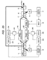
- a signal light outputted from the light source 1 (11) is split into two parts by the branching filter (14).
- Another branching filter (12) is installed between the light source 1 (11) and the branching filter (14), the light propagated in the opposite direction is spectrally separated by this branching filter (14), and the signal light outputted from the light source 1 (11) reaches the photodiode (13).
- the signal light split into two parts by the branching filter (14) reaches the phase modulators A, B (15A, 15B), respectively.
- An electrical signal wherein the bias voltage 1A (22A) is superposed on the data signal A (23A) by the bias superposer (24A), is applied to the phase modulator A (15).
- the lightwave signal inputted into the phase modulator A (15A) is subjected to binary phase modulation by this electrical signal, and the result is outputted.
- the lightwave signal inputted into the phase modulator B (15B) is subjected to binary phase modulation by this electrical signal, and the result is outputted.
- the phase adjuster (16) is installed in the output of the phase modulator B (15B), which is one of the two phase modulators.
- the bias voltage 2 (26) is applied to the phase adjuster (16).
- the phase of the lightwave signal inputted into the phase adjuster (16) is adjusted by an amount according to this bias voltage 2 (26), and is outputted.
- ⁇ /2 is an ideal value.
- the output of the phase modulator A (15A), and the output of the phase adjuster (16), are multiplexed by the multiplexer (17).
- the output of the multiplexer (17) acts as a quaternary phase modulation signal having four phase levels, i.e., + ⁇ /4, +3 ⁇ /4, -3 ⁇ /4 and - ⁇ /4, when the bias of the phase modulator A (15A), phase modulator B (15B), and phase adjuster (16) is ideal.
- the branching filter (18) which extracts part of the outputted light is installed in the output of the multiplexer (17), and the split optical signal reaches the photodiode (19) .
- the photodiode (19) has a frequency response characteristic not exceeding the bit rate.
- the multiplexer (20) that multiplexes the signal light from the light source 2 (21) is further installed in the other output of the branching filter (18).
- the lightwave signal outputted from the light source 1 (11) propagates from the left to the right of the figure, i.e., it reaches the multiplexer (17) via the phase modulator A (15A) or phase modulator B (15B), and the phase adjuster (16) from the branching filter (14), and whereas part thereof is photoelectrically converted by the photodiode (19), the light output from the light source 2 (21) propagates from right to left, i.e., it reaches the branching filter (14) from the multiplexer (17) via the phase modulator A (15A), phase adjuster (16) and phase modulator B (15B), and is finally photoelectrically converted by the photodiode (13).
- V ⁇ of the phase modulator is a value of about 4-6V, and if it is attempted to obtain an amplitude of 2V ⁇ to perform binary phase modulation, a considerably large amplitude signal of 8-12V is required as the drive amplitude. To lower the cost of the transmitter, it is desirable to reduce the amplitude to some extent.
- FIG. 9 shows the modulation situation when the drive amplitude is less than 2V ⁇ . When the modulation amplitude is reduced from 2V ⁇ , the amplitude will be different for each adjacent data. In this case, since the average power is an intermediate value of these different amplitudes, the average power fluctuation accompanying the bias shift actually decreases.
- FIG. 10 shows a simulation result wherein the output of the modulator, i.e., the multiplexer (17), is plotted relative to the bias shift.
- the bias shift is normalized to 2V ⁇ .
- a bias shift amount of 50% is a bias shift amount corresponding to V ⁇ .
- the modulation amplitude is also normalized to 2v ⁇ .
- a modulation amplitude of 100% is a modulation amplitude equivalent to 2V ⁇ , and is the ideal modulation amplitude as shown in FIG. 5 .
- the modulator output also gradually changes. Even if the bias has shifted by 50%, the variation is about 4dB at most, while the modulation amplitude decreases from 100%, and the variation also decreases. Whatever the modulation amplitude is, if the bias shift is 10% or less, the variation is less than 0.2dB and it is difficult to adjust the bias from the modulator output.
- the modulator used for high speed modulation such as 10Gbps or 20Gbps is usually a progressive wave modulator.
- a progressive wave modulator is a modulator which increases the interaction length of an electrical signal and a lightwave signal, and increases the modulation efficiency, when the modulating electrical.signal and the light signal being modulated propagate in the same direction inside the modulator.
- the interaction length decreases, so the modulation efficiency decreases considerably. Specifically, most of the light propagated in the backward direction is output from the modulator without being modulated.
- the relation between the bias voltage and the output light coincides with the extinction characteristic itself.
- the bias voltage can be set to the maximum value.
- a data signal has a spectrum that contains not only high-speed components such as 10GHz and 20GHz, but is continuous from low speed frequencies. Since the interaction length of the aforesaid electrical signal and lightwave signal increases relatively in the case of these low-speed components, even in the case of light which propagates in the opposite direction, it will be modulated by low-speed frequency components.
- FIG. 11 shows the result of a simulation of the relation between bias shift amount and modulator output (in this case, backward light output, i.e., the result monitored by the photodiode (13)), as in the case of FIG.
- the modulation response frequency of the electrical waveform (frequency at which the response characteristics decrease by 3 dB) is 500MHz
- the monitor result changes by as much as 17dB for a bias shift amount of 50%, so the sensitivity of the backward-propagated light output to the bias shift is very high. If the modulation amplitude increases, there is the additional effect that the back-propagated light is modulated by the aforesaid low-frequency components, and the variation of the back-propagated light output decreases.
- the bias of the phase modulator A(15A) can be maintained at an optimum point.
- FIG. 12 is a figure schematically showing the photoelectric field, optical power, and RF Power after reception by the photodiode (19) when the phase difference is ideal, i.e., ⁇ /2, or in the worst case, i.e., when the phase difference is zero.
- the photoelectric field amplitude of the light output is always constant, for example ⁇ 2 as shown in FIG. 12(1) .
- phase difference can be adjusted to ⁇ /2, i.e., the ideal state, by making this monitor result a minimum.
- FIG. 13 shows the result of a simulation of the monitor result of RF power when the phase difference is arranged to be ⁇ /2 or 0.
- a RZ (Return-to-Zero)-DQPSK (Differential QPSK) signal of 40Gbps i.e., a quaternary phase modulation signal
- the RF power when the output was photoelectrically converted by a photodiode was calculated using the bandwidth of the photodiode (horizontal axis) as a parameter.
- the value (vertical axis) of the RF power is a relative value.
- the bias of the phase adjuster (16) can be maintained at an optimum point.
- FIG. 14 is a figure describing the effect of another bias control of the bias characteristic of the phase adjuster (16).
- This diagram is an experimental result which measured the modulation output of a RZ-DQPSK signal of 40Gbps using a photodiode of 2.5GHz bandwidth, while varying the bias of the phase adjuster.
- An evaluation was performed for three bias states of the two phase modulators, i.e., (1) both optimum values, (2) an intermediate value between both optimum values and both worst values, (3) one worst value and one optimum value.
- the amplitude of the variation characteristic of monitor power changes with the bias states of the two phase modulators, but the bias voltage in a valley, i.e., the control convergence point when minimization control is performed, hardly changes at all.
- the bias control of the phase adjuster the effect of the bias state of the two phase modulators is minor.
- Figs. 15, 16 , and 17 are diagrams describing the effect of another bias control on the bias characteristic of the phase modulator 1A (15A).
- FIG. 14 these are also experimental results obtained by measuring the monitor output of the backward light of a RZ-DQPSK signal of 40Gbps, while varying the bias of the phase modulator. An evaluation was performed for three bias states of the other phase modulator, i.e., (1) the optimum value, (2) an intermediate value between the optimum value and the worst value, (3) the worst value.
- FIG. 15 shows the optimum value
- FIG. 16 shows an intermediate value between the optimum value and the worst value
- FIG. 17 shows the worst value.
- the bias 1A is a minimum value in the vicinity of -2.5V regardless of the bias state 1B.
- the control convergence point when the bias 1A is subjected to minimization control hardly changes at all even if the bias 1B changes, and the bias 1B and bias 1A can be minimization-controlled independently.
- the situation is different when the bias 2 is an intermediate value.
- the minimum value of the bias 1A changes according to the value of the bias 1B
- the bias 1B shifts from the optimum value to the worst value
- the minimum value of the bias 1A shifts to the negative side.
- the control convergence point when the bias 1A is minimization-controlled depends on the bias 1B.
- the bias 1A and bias 1B are controlled independently, the mutual control convergence point changes due to the effect of the interaction, and the output waveform changes in an unstable manner without the control converging. Referring to FIG. 17 , it is seen that this tendency becomes even stronger when the bias 2 is the worst value.
- the bias control of the phase adjuster is hardly affected by the bias of the two phase modulators, the bias control of the two phase modulators is strongly affected by the bias of the phase period. The reason can be understood from the schematic diagrams shown in FIG. 18 and FIG. 19 .
- FIG. 18 is a schematic diagram showing the situation of the backward light when the bias 2 is an optimum value, i.e., when the phase difference is ⁇ /2, and the two phase modulation components are orthogonal.
- the backward light which penetrates the phase modulator A(15A) is represented by a vector A
- the backward light which penetrates the phase modulator B(15B) is represented by a vector B.
- the vector lengths of the vector A and vector B represent the light intensity.
- the vector A and vector B are subject to a combined electric field, i.e., a combined vector, in the branching filter (14).
- the light received by the photodiode (13) is a vector shown by the dotted line, i.e., a combined vector of the vector A and vector B.
- the bias of the phase modulator A (15A) is adjusted while the bias of the phase modulator B (15B) is fixed at a specified value.
- This operation is equivalent to the operation, in FIG. 18 , of changing the length of the vector A while the length of the vector B is fixed.
- the operation of monitoring the intensity of the photodiode (13), is equivalent to an operation which measures the length of the combined vector.
- the operation of adjusting the bias of the phase modulator A (15A) so that the backward light is a minimum is equivalent to the operation of adjusting the length of the vector A so that the length of the combined vector is minimized.
- the length of the vector A changes from a positive to a negative value in Case 1, Case 2, and Case 3, of FIG. 18 , the length of the combined vector is a minimum when the vector A is a zero vector.
- the vector A can be minimized regardless of the state of vector B, therefore the bias of the phase modulator A and phase modulator B can be minimization-controlled independently.
- the length of the vector A at this time depends on the length of the vector B when the angle (the acute angle side is selected) made by the two vectors is ⁇ , except for the case where ⁇ is ⁇ /2, since cos ⁇ is multiplied by the length of the vector B. Specifically, this means that when they do not intersect perpendicularly, the control convergence point of the phase modulator A varies according to the bias of the phase modulator B. It is seen that, whereas in the bias control of the phase adjuster, there is hardly any effect due to the bias of the two phase modulators, in the bias control of the two phase modulators, there is a strong effect due to the bias of the phase period.
- phase adjuster (16) of the quaternary phase modulator shown in FIG. 8 and the two phase modulators (15A, 15B), by performing control according to the flowchart shown in FIG. 20 .
- Control 2 bias control of the phase adjuster, i.e., control of orthogonality
- Control 1 bias control of the phase modulator
- the phase adjuster and phase modulator can be controlled without being affected by the other phase modulator and phase adjuster, which was described referring to FIG. 15, FIG. 16 , FIG. 17 , FIG. 18 and FIG. 19 .
- the present invention not only compensates a bias drift of the phase modulators or the phase adjuster, but it is also effective for absorbing individual variations in the ideal characteristics of the phase modulators or phase adjuster, effective for controlling a shift from a voltage of zero volts, for control in the case of starting from a preset initial value (default value) and bringing the device to operational stability, and particularly effective for control in the case of starting up a device.
- the minimization control shown in FIG. 21 is suitable, for example.
- a 2 variable control such as Control 1
- sequential control which first minimizes the bias 1A and then minimizes the bias 1B is appropriate.
- the mountain climbing method wherein the bias 1A and bias 1B are respectively made to vary by ⁇ A, ⁇ B, and the next ⁇ A, ⁇ B at which the slope is a maximum together with the variation amount in the monitor result are sequentially calculated repeatedly.
- a laser light source or a LED light source may be used. If the spontaneous emission light from an erbium addition amplifier (EDFA, 32) is used, as shown in FIG. 24 , there is the advantage that the polarized wave adjustment of the backward light and phase modulator can be omitted.
- EDFA erbium addition amplifier
- part of the signal light source may be split by the branching filter (31) and looped back to substitute for the backward light source.
- part of the signal light may be reflected by a reflector (33) and reversed to substitute for the backward light source.
- phase modulator B(15B) and phase adjuster (16) there is no predominant difference in the arrangement order of the phase modulator B(15B) and phase adjuster (16), and even if the phase adjuster (16) is arranged ahead of the phase modulator B(15B), this patent can still be applied satisfactorily. It can likewise be applied to the other embodiments shown below.
- the present invention can apply any material, e.g., a semiconductor such as LiNbO 3 (lithium niobate), GaAs or InP.
- a semiconductor such as LiNbO 3 (lithium niobate), GaAs or InP.
- phase modulators and phase adjuster may likewise be applied when the phase modulators and phase adjuster are formed on an integrated waveguide path, or when they are manufactured by connecting individual components, and may likewise be applied in the other embodiments shown below.
- phase adjuster (16) of the quaternary phase modulator and the two phase modulators (15A, 15B) shown in FIG. 8 can be stably controlled by performing control according to the flowchart of FIG. 27 .
- the difference in the control time constant if the difference is about for example one order of magnitude, as in the case t1>10xt2, there is no problem as regards stable operation. Further, if there is a certain degree of restriction on the time constant such as the limit of a sample hold circuit, the invention may still be applied without a problem even if the restriction is several orders of magnitude.
- FIG. 28 in addition to the composition of FIG. 8 , a circuit (29A) which superposes a low-speed frequency fA (28A) on the bias 1A, and a circuit (29B) which superposes a low-speed frequency fB (28B) on the bias 1B are provided, and the electrical bandpass filter (30) is also added to the output of the photodiode (19).
- Control 1 in FIG. 28 is the same as that of the first embodiment.
- a sum (fA+fB) or a difference (fA-fB) of two low frequency signals is extracted by the electrical bandpass filter (30) installed in the output of the photodiode (19), and the bias 2 (26) of the phase adj uster (16) is controlled so that the absolute value is a minimum, or does not exceed a predetermined specific value.
- Control 2 may be performed with higher precision.
- phase adjuster (16) and the two phase modulators (15A, 15B) of the quaternary phase modulator shown in FIG. 28 can be stably controlled by performing control according to the flowchart of FIG. 20 .
- Control 2 bias control of the phase adjuster, i.e., control of orthogonality
- Control 1 bias control of the phase modulator
- the bias of each phase modulator is controlled while maintaining orthogonality.
- the phase adjuster and phase modulators can be controlled without being affected by the other phase modulator and phase adjuster.
- phase adjuster (16) and the two phase modulators (15A, 15B) of the quaternary phase modulator shown in FIG. 28 can be stably controlled by performing control according to the flowchart of FIG. 27 .
- control 1 control of the bias of the phase modulator
- control 2 control of the bias of the phase adjuster, i.e., control of orthogonality
- t2 control of the bias of the phase adjuster
- Control 1 is the same as that of Examples 1 and 3.
- a sum (fA+fB) or a difference (fA-fB)) of two low frequency signals is extracted by an electrical bandpass filter (30) installed in the output of the photodiode (13), and the bias 2(26) of the phase adjuster (16) is controlled so that the absolute value is a minimum, or does not exceed a predetermined specific value.
- Control 2 may be performed with higher precision.
- phase adjuster (16) and the two phase modulators (15A, 15B) of the quaternary phase modulator shown in FIG. 29 can be stably controlled.
- Control 2. bias control of the phase adjuster, i.e., control of orthogonality
- Control 1 bias control of the phase modulator
- the bias of each phase modulator is controlled while maintaining orthogonality.
- the phase adjuster and phase modulators can be controlled without being affected by the other phase modulator and phase adjuster.
- FIG. 29 A sixth embodiment of the present invention will now be described referring FIG. 29 and FIG. 27 .
- the phase adjuster (16) and the two phase modulators (15A, 15B) of the quaternary phase modulator shown in FIG. 29 can be stably controlled by performing control according to the flowchart of FIG. 27 .
Landscapes
- Physics & Mathematics (AREA)
- Optics & Photonics (AREA)
- Engineering & Computer Science (AREA)
- Computer Networks & Wireless Communication (AREA)
- Signal Processing (AREA)
- Nonlinear Science (AREA)
- Electromagnetism (AREA)
- General Physics & Mathematics (AREA)
- Optical Modulation, Optical Deflection, Nonlinear Optics, Optical Demodulation, Optical Logic Elements (AREA)
- Optical Communication System (AREA)
- Digital Transmission Methods That Use Modulated Carrier Waves (AREA)
Applications Claiming Priority (1)
| Application Number | Priority Date | Filing Date | Title |
|---|---|---|---|
| JP2007250368A JP4934557B2 (ja) | 2007-09-27 | 2007-09-27 | 4値位相変調器 |
Publications (2)
| Publication Number | Publication Date |
|---|---|
| EP2042913A2 true EP2042913A2 (fr) | 2009-04-01 |
| EP2042913A3 EP2042913A3 (fr) | 2011-04-06 |
Family
ID=40138707
Family Applications (1)
| Application Number | Title | Priority Date | Filing Date |
|---|---|---|---|
| EP08013952A Withdrawn EP2042913A3 (fr) | 2007-09-27 | 2008-08-04 | Modulateur optique de phase par déplacement de phase en quadrature |
Country Status (4)
| Country | Link |
|---|---|
| US (1) | US8095018B2 (fr) |
| EP (1) | EP2042913A3 (fr) |
| JP (1) | JP4934557B2 (fr) |
| CN (1) | CN101399613B (fr) |
Cited By (4)
| Publication number | Priority date | Publication date | Assignee | Title |
|---|---|---|---|---|
| WO2012144082A1 (fr) * | 2011-04-19 | 2012-10-26 | Nec Corporation | Émetteur optique et son procédé de commande |
| WO2013140634A1 (fr) * | 2012-03-22 | 2013-09-26 | Nec Corporation | Émetteur optique et son procédé de commande |
| US20180074386A1 (en) * | 2016-09-09 | 2018-03-15 | Huawei Technologies Canada Co., Ltd. | Method and apparatus for monitoring and controlling a photonic switch using phase sweeping |
| US10177852B2 (en) | 2015-05-04 | 2019-01-08 | Plugtech Precision Systems Limited (Shenzhen) | Method and apparatus for automatically controlling bias voltage of optical modulator |
Families Citing this family (27)
| Publication number | Priority date | Publication date | Assignee | Title |
|---|---|---|---|---|
| US7912378B2 (en) * | 2007-01-26 | 2011-03-22 | Fujitsu Limited | Modulating a signal using a fractional phase modulator |
| JP4946833B2 (ja) * | 2007-11-30 | 2012-06-06 | 富士通オプティカルコンポーネンツ株式会社 | 光変調装置 |
| TWI382684B (zh) * | 2008-11-07 | 2013-01-11 | Univ Nat Chiao Tung | Dual Service Fiber Capture System |
| US20100142964A1 (en) * | 2008-12-08 | 2010-06-10 | Sun-Hyok Chang | Optical transmission apparatus with stable optical signal output |
| JP5374709B2 (ja) * | 2009-08-07 | 2013-12-25 | 株式会社日立製作所 | 光送信器 |
| US9020361B2 (en) * | 2009-09-08 | 2015-04-28 | Nippon Telegraph And Telephone Corporation | Optical signal transmitter, and bias voltage control method |
| JP5421792B2 (ja) * | 2010-01-12 | 2014-02-19 | 株式会社日立製作所 | 偏波多重送信器及び伝送システム |
| EP2541806B1 (fr) * | 2010-02-25 | 2018-03-28 | Mitsubishi Electric Corporation | Transmetteur optique |
| JP5506575B2 (ja) * | 2010-07-08 | 2014-05-28 | 三菱電機株式会社 | 光変調器、光送信装置およびバイアス調整方法 |
| JP5853386B2 (ja) | 2010-12-16 | 2016-02-09 | 富士通オプティカルコンポーネンツ株式会社 | 光変調装置および光変調制御方法 |
| CN102156499B (zh) * | 2011-04-06 | 2013-06-19 | 烽火通信科技股份有限公司 | 基于对数检波的光相位延迟器的偏置控制方法与装置 |
| CN102201868B (zh) * | 2011-04-06 | 2014-01-01 | 烽火通信科技股份有限公司 | 双并联mz调制器的偏置控制方法与装置 |
| JP2013089754A (ja) * | 2011-10-18 | 2013-05-13 | Sumitomo Electric Ind Ltd | 波長可変半導体レーザの制御方法 |
| JP2013183455A (ja) * | 2012-02-29 | 2013-09-12 | Zte (Usa) Inc | ナイキスト波長分割多重システム |
| US9344194B2 (en) * | 2013-02-21 | 2016-05-17 | Fujitsu Limited | System and method for monitoring and control of an optical modulator for an M-QAM transmitter |
| US10192017B2 (en) * | 2015-04-28 | 2019-01-29 | Teledyne Signal Processing Devices Sweden Ab | Drift compensation |
| JP6368295B2 (ja) * | 2015-05-18 | 2018-08-01 | 日本電信電話株式会社 | 光送信器 |
| CN108028702B (zh) * | 2015-09-22 | 2021-04-30 | 英特尔公司 | 采用差分偏置控制的电光调制器 |
| CN105302019A (zh) * | 2015-10-13 | 2016-02-03 | 电子科技大学 | 一种电光调制器偏置工作点控制装置及方法 |
| CN106301554B (zh) * | 2016-08-31 | 2019-01-22 | 武汉光迅科技股份有限公司 | 一种并联mzi电光调制器工作点电压的调试方法及调试装置 |
| CN108667520B (zh) * | 2017-03-31 | 2020-12-29 | 富士通株式会社 | 光发射机调制器的偏置控制装置及方法、光发射机 |
| JP6961986B2 (ja) * | 2017-04-07 | 2021-11-05 | 富士通オプティカルコンポーネンツ株式会社 | 光送信機、及び光伝送方法 |
| US10707837B2 (en) * | 2017-07-06 | 2020-07-07 | Analog Photonics LLC | Laser frequency chirping structures, methods, and applications |
| CN110870225B (zh) * | 2017-07-14 | 2022-07-26 | 日本电信电话株式会社 | 偏压控制电路和偏压控制方法 |
| CN109581701A (zh) * | 2018-12-12 | 2019-04-05 | 北京中创为量子通信技术有限公司 | 一种光强度调制的实时维稳系统及方法 |
| US11216024B1 (en) * | 2021-03-20 | 2022-01-04 | Sitrus Technology Corporation | Referenceless frequency acquisition |
| CN116699880A (zh) * | 2022-02-25 | 2023-09-05 | 苏州极刻光核科技有限公司 | 电光调制器 |
Citations (1)
| Publication number | Priority date | Publication date | Assignee | Title |
|---|---|---|---|---|
| US7266306B1 (en) | 2003-10-03 | 2007-09-04 | Nortel Networks Limited | Method for optical carrier suppression and quadrature control |
Family Cites Families (10)
| Publication number | Priority date | Publication date | Assignee | Title |
|---|---|---|---|---|
| JP2869585B2 (ja) * | 1991-02-18 | 1999-03-10 | 日本電信電話株式会社 | 光変調装置 |
| JP3841261B2 (ja) * | 2000-09-11 | 2006-11-01 | 三菱電機株式会社 | 位相変調装置及び位相変調方法 |
| GB2370473B (en) | 2000-12-21 | 2004-04-07 | Marconi Caswell Ltd | Improvements in or relating to optical communication |
| CN1223133C (zh) * | 2002-05-15 | 2005-10-12 | 华为技术有限公司 | 光信号调制方法、波分复用光传输系统中传输方法及系统 |
| US7314640B2 (en) * | 2003-07-11 | 2008-01-01 | Mongkol Sriwongjanya | Formulation and process for drug loaded cores |
| JP4814494B2 (ja) * | 2004-03-30 | 2011-11-16 | 株式会社日立製作所 | 光波長挿入分岐装置 |
| JP4440091B2 (ja) * | 2004-12-24 | 2010-03-24 | 住友大阪セメント株式会社 | 光変調器 |
| JP2007163941A (ja) * | 2005-12-15 | 2007-06-28 | Nippon Telegr & Teleph Corp <Ntt> | 4相位相変調回路 |
| JP4910388B2 (ja) * | 2005-12-22 | 2012-04-04 | 株式会社日立製作所 | 光変調装置、光送信器、及び光伝送装置 |
| JP4563944B2 (ja) * | 2006-01-31 | 2010-10-20 | 富士通株式会社 | 光送信器 |
-
2007
- 2007-09-27 JP JP2007250368A patent/JP4934557B2/ja not_active Expired - Fee Related
-
2008
- 2008-08-04 EP EP08013952A patent/EP2042913A3/fr not_active Withdrawn
- 2008-08-12 US US12/222,574 patent/US8095018B2/en not_active Expired - Fee Related
- 2008-08-13 CN CN2008102106382A patent/CN101399613B/zh not_active Expired - Fee Related
Patent Citations (1)
| Publication number | Priority date | Publication date | Assignee | Title |
|---|---|---|---|---|
| US7266306B1 (en) | 2003-10-03 | 2007-09-04 | Nortel Networks Limited | Method for optical carrier suppression and quadrature control |
Non-Patent Citations (1)
| Title |
|---|
| KENRO SEKINE ET AL.: "A Novel Bias Control Technique for MZ Modulator with Monitoring Power of Backward Light for Advanced Modulation Formats", OPTICAL FIBER COMMUNICATION CONFERENCE AND EXPOSITION NATIONAL FIBER OPTIC ENGINEERS CONFERENCE, OFCNFOEC, 1 March 2007 (2007-03-01), pages 1 - 3 |
Cited By (7)
| Publication number | Priority date | Publication date | Assignee | Title |
|---|---|---|---|---|
| WO2012144082A1 (fr) * | 2011-04-19 | 2012-10-26 | Nec Corporation | Émetteur optique et son procédé de commande |
| US9166697B2 (en) | 2011-04-19 | 2015-10-20 | Nec Corporation | Optical transmitter and method for controlling the same |
| WO2013140634A1 (fr) * | 2012-03-22 | 2013-09-26 | Nec Corporation | Émetteur optique et son procédé de commande |
| US9544060B2 (en) | 2012-03-22 | 2017-01-10 | Nec Corporation | Optical transmitter and method for controlling the same |
| US10177852B2 (en) | 2015-05-04 | 2019-01-08 | Plugtech Precision Systems Limited (Shenzhen) | Method and apparatus for automatically controlling bias voltage of optical modulator |
| US20180074386A1 (en) * | 2016-09-09 | 2018-03-15 | Huawei Technologies Canada Co., Ltd. | Method and apparatus for monitoring and controlling a photonic switch using phase sweeping |
| US10209537B2 (en) * | 2016-09-09 | 2019-02-19 | Huawei Technologies Canada Co., Ltd. | Method and apparatus for monitoring and controlling a photonic switch using phase sweeping |
Also Published As
| Publication number | Publication date |
|---|---|
| US20090092401A1 (en) | 2009-04-09 |
| JP4934557B2 (ja) | 2012-05-16 |
| JP2009081747A (ja) | 2009-04-16 |
| US8095018B2 (en) | 2012-01-10 |
| CN101399613A (zh) | 2009-04-01 |
| EP2042913A3 (fr) | 2011-04-06 |
| CN101399613B (zh) | 2012-01-04 |
Similar Documents
| Publication | Publication Date | Title |
|---|---|---|
| US8095018B2 (en) | Quaternary phase modulator | |
| US9419720B2 (en) | Optical signal transmitter | |
| US7907324B2 (en) | Optical modulator and controlling method and apparatus thereof | |
| US8412047B2 (en) | Polarization multiplexed light transmitter and control method thereof | |
| US7068948B2 (en) | Generation of optical signals with return-to-zero format | |
| US7869719B2 (en) | Method and system for automatic feedback control for fine tuning a delay interferometer | |
| EP2267923B1 (fr) | Système de transmission optique | |
| CA2588585C (fr) | Procede et appareil de controle de polarisation et d'alignement dans un emetteur de signal optique | |
| US20070146860A1 (en) | Optical modulation device, optical transmitter, and optical transmission equipment | |
| US8103173B2 (en) | Method and system for a polarization mode dispersion tolerant optical homodyne detection system with optimized transmission modulation | |
| US9614639B2 (en) | Power control of optical signals having different polarizations | |
| JP4675796B2 (ja) | 自動分散補償型光伝送システム | |
| JP5198996B2 (ja) | 光変調器 | |
| Corzine et al. | 10-channel× 40Gb/s per channel DQPSK monolithically integrated InP-based transmitter PIC | |
| KR100547781B1 (ko) | 편광 듀오바이너리 광전송장치 | |
| JP2013174761A (ja) | 光送信器、光通信システムおよび光送信方法 | |
| JP4836839B2 (ja) | 光角度変調器 | |
| EP1873575A1 (fr) | Appareil de modulation optique et méthode de control de l'appareil | |
| KR101367407B1 (ko) | 단측파대 광송신장치 | |
| US11429007B2 (en) | Electro-optical modulator and method of modulating an optical beam to carry an RF signal | |
| EP1524548A1 (fr) | Système de stabilisation d'un modulateur optique pour signaux RZ | |
| EP1641151A1 (fr) | Procédé et dispositif de génération d'un signal optique à quatre niveaux | |
| JP5630512B2 (ja) | 光変調器 | |
| Han et al. | Novel method for monitoring principal state of polarization for PMD compensation |
Legal Events
| Date | Code | Title | Description |
|---|---|---|---|
| PUAI | Public reference made under article 153(3) epc to a published international application that has entered the european phase |
Free format text: ORIGINAL CODE: 0009012 |
|
| AK | Designated contracting states |
Kind code of ref document: A2 Designated state(s): AT BE BG CH CY CZ DE DK EE ES FI FR GB GR HR HU IE IS IT LI LT LU LV MC MT NL NO PL PT RO SE SI SK TR |
|
| AX | Request for extension of the european patent |
Extension state: AL BA MK RS |
|
| RAP1 | Party data changed (applicant data changed or rights of an application transferred) |
Owner name: HITACHI, LTD. |
|
| 17P | Request for examination filed |
Effective date: 20100331 |
|
| PUAL | Search report despatched |
Free format text: ORIGINAL CODE: 0009013 |
|
| AK | Designated contracting states |
Kind code of ref document: A3 Designated state(s): AT BE BG CH CY CZ DE DK EE ES FI FR GB GR HR HU IE IS IT LI LT LU LV MC MT NL NO PL PT RO SE SI SK TR |
|
| AX | Request for extension of the european patent |
Extension state: AL BA MK RS |
|
| AKX | Designation fees paid |
Designated state(s): AT BE BG CH CY CZ DE DK EE ES FI FR GB GR HR HU IE IS IT LI LT LU LV MC MT NL NO PL PT RO SE SI SK TR |
|
| 17Q | First examination report despatched |
Effective date: 20141020 |
|
| STAA | Information on the status of an ep patent application or granted ep patent |
Free format text: STATUS: THE APPLICATION IS DEEMED TO BE WITHDRAWN |
|
| 18D | Application deemed to be withdrawn |
Effective date: 20150303 |