EP2022590B1 - Wave soldering tank - Google Patents
Wave soldering tank Download PDFInfo
- Publication number
- EP2022590B1 EP2022590B1 EP07740811A EP07740811A EP2022590B1 EP 2022590 B1 EP2022590 B1 EP 2022590B1 EP 07740811 A EP07740811 A EP 07740811A EP 07740811 A EP07740811 A EP 07740811A EP 2022590 B1 EP2022590 B1 EP 2022590B1
- Authority
- EP
- European Patent Office
- Prior art keywords
- casing
- screw pump
- wave soldering
- soldering tank
- pump
- Prior art date
- Legal status (The legal status is an assumption and is not a legal conclusion. Google has not performed a legal analysis and makes no representation as to the accuracy of the status listed.)
- Active
Links
- 238000005476 soldering Methods 0.000 title claims abstract description 59
- 229910000679 solder Inorganic materials 0.000 abstract description 66
- 230000010349 pulsation Effects 0.000 abstract description 18
- 208000028659 discharge Diseases 0.000 description 25
- 238000003780 insertion Methods 0.000 description 11
- 230000037431 insertion Effects 0.000 description 11
- 239000007788 liquid Substances 0.000 description 9
- 230000008602 contraction Effects 0.000 description 4
- 230000000694 effects Effects 0.000 description 3
- 230000005484 gravity Effects 0.000 description 3
- 230000003647 oxidation Effects 0.000 description 3
- 238000007254 oxidation reaction Methods 0.000 description 3
- 230000000052 comparative effect Effects 0.000 description 2
- 238000000926 separation method Methods 0.000 description 2
- 241000237858 Gastropoda Species 0.000 description 1
- 229910020220 Pb—Sn Inorganic materials 0.000 description 1
- 230000015572 biosynthetic process Effects 0.000 description 1
- 238000001816 cooling Methods 0.000 description 1
- 239000012530 fluid Substances 0.000 description 1
- 230000004907 flux Effects 0.000 description 1
- 238000004519 manufacturing process Methods 0.000 description 1
- 230000008018 melting Effects 0.000 description 1
- 238000002844 melting Methods 0.000 description 1
- 238000005086 pumping Methods 0.000 description 1
- 238000007711 solidification Methods 0.000 description 1
- 230000008023 solidification Effects 0.000 description 1
Images


Classifications
-
- B—PERFORMING OPERATIONS; TRANSPORTING
- B23—MACHINE TOOLS; METAL-WORKING NOT OTHERWISE PROVIDED FOR
- B23K—SOLDERING OR UNSOLDERING; WELDING; CLADDING OR PLATING BY SOLDERING OR WELDING; CUTTING BY APPLYING HEAT LOCALLY, e.g. FLAME CUTTING; WORKING BY LASER BEAM
- B23K3/00—Tools, devices, or special appurtenances for soldering, e.g. brazing, or unsoldering, not specially adapted for particular methods
- B23K3/06—Solder feeding devices; Solder melting pans
- B23K3/0646—Solder baths
- B23K3/0653—Solder baths with wave generating means, e.g. nozzles, jets, fountains
-
- B—PERFORMING OPERATIONS; TRANSPORTING
- B23—MACHINE TOOLS; METAL-WORKING NOT OTHERWISE PROVIDED FOR
- B23K—SOLDERING OR UNSOLDERING; WELDING; CLADDING OR PLATING BY SOLDERING OR WELDING; CUTTING BY APPLYING HEAT LOCALLY, e.g. FLAME CUTTING; WORKING BY LASER BEAM
- B23K1/00—Soldering, e.g. brazing, or unsoldering
- B23K1/0008—Soldering, e.g. brazing, or unsoldering specially adapted for particular articles or work
- B23K1/0016—Brazing of electronic components
-
- B—PERFORMING OPERATIONS; TRANSPORTING
- B23—MACHINE TOOLS; METAL-WORKING NOT OTHERWISE PROVIDED FOR
- B23K—SOLDERING OR UNSOLDERING; WELDING; CLADDING OR PLATING BY SOLDERING OR WELDING; CUTTING BY APPLYING HEAT LOCALLY, e.g. FLAME CUTTING; WORKING BY LASER BEAM
- B23K1/00—Soldering, e.g. brazing, or unsoldering
- B23K1/08—Soldering by means of dipping in molten solder
- B23K1/085—Wave soldering
-
- H—ELECTRICITY
- H05—ELECTRIC TECHNIQUES NOT OTHERWISE PROVIDED FOR
- H05K—PRINTED CIRCUITS; CASINGS OR CONSTRUCTIONAL DETAILS OF ELECTRIC APPARATUS; MANUFACTURE OF ASSEMBLAGES OF ELECTRICAL COMPONENTS
- H05K3/00—Apparatus or processes for manufacturing printed circuits
- H05K3/30—Assembling printed circuits with electric components, e.g. with resistor
- H05K3/32—Assembling printed circuits with electric components, e.g. with resistor electrically connecting electric components or wires to printed circuits
- H05K3/34—Assembling printed circuits with electric components, e.g. with resistor electrically connecting electric components or wires to printed circuits by soldering
- H05K3/3457—Solder materials or compositions; Methods of application thereof
- H05K3/3468—Applying molten solder
-
- B—PERFORMING OPERATIONS; TRANSPORTING
- B23—MACHINE TOOLS; METAL-WORKING NOT OTHERWISE PROVIDED FOR
- B23K—SOLDERING OR UNSOLDERING; WELDING; CLADDING OR PLATING BY SOLDERING OR WELDING; CUTTING BY APPLYING HEAT LOCALLY, e.g. FLAME CUTTING; WORKING BY LASER BEAM
- B23K2101/00—Articles made by soldering, welding or cutting
- B23K2101/36—Electric or electronic devices
- B23K2101/42—Printed circuits
Definitions
- This invention relates to a wave soldering tank which is installed in an automatic soldering apparatus and which carries out soldering of printed circuit boards.
- processing equipment such as a fluxer, a preheater, a wave soldering tank, and a cooler are arranged in series, and a conveyor runs above the processing equipment. While being transported by the conveyor, a printed circuit board undergoes flux application in the fluxer, preheating in the preheater, adhesion of solder in the wave soldering tank, and cooling in the cooler to carry out soldering.
- the wave soldering tank must not have pulsing in which the height of spouted solder moves up and down, and oxides which are floating in molten solder must not be enveloped therein.
- a wave soldering tank carries out soldering by spouting molten solder upwards and contacting a printed circuit board with the spouted molten solder.
- a wave soldering tank requires a discharge pump for pumping molten solder and a discharge nozzle for upwardly spouting molten solder which is sent to it by the pump.
- the discharge pump and the discharge nozzle are connected by a duct.
- the discharge pump is provided at one end of the duct, and the discharge nozzle is installed at the other end of the duct.
- the discharge pump is installed inside a casing formed at the end of the duct. The discharge pump sucks in molten solder and sends the molten solder to the discharge nozzle through the duct, and it spouts molten solder upwards from the discharge nozzle.
- An impeller pump has a large number of plate-shaped blades radially installed on the periphery of a shaft.
- the casing of an impeller pump is formed at one end of a duct and has roughly the shape of a snail.
- the shaft of an impeller pump passes through a shaft hole formed in the top of the casing and projects above the surface of molten solder.
- An inlet of the casing is formed in the bottom of the casing.
- the impeller pump merely has blades radially installed on a shaft, so it is easy to manufacture and inexpensive.
- An impeller pump causes the pulsation of molten solder since the molten solder is pumped discontinuously.
- a screw pump has one or more plate-shaped members helically wrapped around the periphery of a shaft. Molten solder rests on and is transported by the helical plate-shaped members. Accordingly, a screw pump does not have discontinuous operation, and theoretically it does not cause pulsations. From long in the past, there have been many proposals in patents and utility models of wave soldering tanks using screw pumps (see US-A-4 700 878 as well as Patent Documents 1 - 7).
- an inlet R is formed by the inner surface of a cylindrical casing K. Because the inner diameter R 2 of the inlet R is larger than the diameter P 1 of the screw pump P, a wide gap G is formed between the screw pump P and the casing K.
- molten solder which is sucked into the inlet R in the bottom of the casing attempts to flow along the duct D towards the discharge nozzle (as shown by arrow b), but it is pushed back by the resistance of molten solder which is already present inside the duct.
- the molten solder which is pushed back flows backward as shown by arrow c through the gap G between the screw pump P and the casing K and flows outwards from the inlet R.
- the molten solder which flows outwards interferes with molten solder which is being sucked in by the screw pump P (arrow a) and disturbs the molten solder which is being sucked in.
- the turbulent molten solder which is sucked in is pushed out by the screw pump P, it remains turbulent, and the turbulence is thought to cause pulsation when the solder is spouted from the discharge nozzle.
- molten solder in upper portions does not undergo reverse flow downwards through the gap if the gap is 0.5 mm or less. It is possible to precisely form the diameter of the screw pump and the diameter of the casing so as to eliminate this gap. However, objects installed inside a wave soldering tank are invariably deformed. Therefore, even if the gap is finished to 0.5 mm, for example, a screw pump installed inside the casing will become eccentric and end up contacting the casing.
- a heater inside the wave soldering tank is energized and solder is maintained in a molten state.
- the heater no longer is energized, and the solder which had melted cools and solidifies.
- the heater is again made to conduct and solder is heated and melted. In this manner, melting and solidification of solder are repeatedly carried out in a wave soldering tank. Solder thermally expands when it is heated by the heater, and it thermally contracts when the heater stops being energized and the solder cools. Therefore, objects inside a wave soldering tank are subjected to the thermal expansion and contraction of solder and are deformed.
- a casing or a screw pump installed inside a casing is also subjected to the thermal expansion and contraction of solder and deforms.
- the screw pump becomes eccentric and rubs against the casing or is strongly pressed against the casing and can no longer smoothly rotate.
- pulsation take place, but the screw pump or the casing is damaged.
- the inlet for molten solder in the bottom of the casing has the same diameter as the inner diameter of the casing, so molten solder which flows in reverse from above as shown by arrow c in Figure 5 flows downwardly outwards and causes turbulence of molten solder which is sucked into the screw pump P (arrow a).
- the present inventors discovered that if reverse flow can be prevented, pulsation no longer takes place even in a wave soldering tank having a large gap between a screw pump and a casing, and they completed the present invention.
- the present invention is a wave soldering tank according to claim 1.
- the upper portion of the casing is an arcuate outlet having a portion which faces in the direction of the duct, and outwardly flaring guide walls are formed on both sides of the outlet.
- outwardly flaring guide walls are installed at the outlet of the casing to provide stable fluid flow in a soldering tank using a screw pump.
- the upper portion of the casing has an arcuate portion which opens in the direction of flow, and outwardly flaring guide walls are installed on both sides of the arc.
- a wave soldering tank according to the present invention does not require precise finishing of the gap between the screw pump and a casing, and it can be inexpensively manufactured. According to the present invention, even if the screw pump or the casing deforms to a certain extent due to thermal expansion and contraction of solder, the screw pump does not rub against and is not pressed against the casing, and the screw pump can stably rotate. In a wave soldering tank according to the present invention, as the diameter of the inlet formed in the bottom of the casing is smaller than the diameter of the screw pump, when molten solder which is sucked in by the screw pump flows backwards between the screw pump and the casing, it is obstructed by the inner flange of the inlet and does not flow out from the inlet.
- molten solder which is sucked in by the screw pump does not become turbulent. Therefore, it does not become turbulent when it leaves the screw pump and flows through the duct, and it does not undergo pulsation when it spouts from the discharge nozzle.
- a wave soldering tank according to the present invention can always stably contact molten solder with the surface to be soldered of a printed circuit board, and reliable soldered portions are obtained.
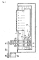
- Figure 1 is a front cross-sectional view of a wave soldering tank according to the present invention
- Figure 2 is an enlarged partially cross-sectional perspective view of important portions
- Figure 3 is a cross-sectional view taken along line X-X of Figure 1
- Figure 4 is a view for explaining the flow of molten solder in a screw pump of a wave soldering tank according to the present invention.
- a wave soldering tank according to the present invention has a lidless box-shaped body 1.
- a duct 2 is installed inside the body.
- a casing 3 is installed at one end of the duct 2, and a discharge nozzle 4 is installed at the upper portion of the other end.
- a screw pump 5 is installed inside the casing 3 with a suitable gap G, such as a gap of a size such that the screw pump will not contact the casing even if the screw pump develops a certain amount of eccentricity due to thermal expansion and contraction of solder.
- An inlet 6 is formed in the bottom of the casing 3.
- the inlet 6 is formed by an inner flange 7 at the bottom of the casing 3.
- the diameter R 1 of the inlet 6 is smaller than the diameter P 1 of the screw pump.
- the upper portion of the casing 3 is partially cut away to form an arcuate outlet 8.
- Outwardly flaring guide walls 9, 9 are formed on both sides of the outlet 8.
- the ends of the guide walls are secured to both walls 10, 10 of the duct 2.
- a portion which is flush with the outlet 8 forms a guide plate 11, and the lower portion of the guide plate is secured to the bottom surface 12 of the duct 2.
- the duct 2 which forms the top of the casing 3 has a pump insertion hole 13 having roughly the same diameter as the inner diameter of the casing 3, and a shaft holding member 14 is installed above the pump insertion hole.
- a pump shaft 16 which is secured to the screw pump 5 at its lower end and to a pulley 15 at its upper end is rotatably mounted on the shaft holding member 14.
- the shaft holding member 14 is constituted by a lower plate 17, an upper plate 18, four pipes 19, four nuts 20, two bearings 21 and 21, and an inlay board 22.
- the lower plate 17 and the upper plate 18 are connected by the four pipes 19.
- the pipes 19 have a length such that when the shaft holding member 14 is disposed atop the duct 2, the pipes project upwards from the liquid surface of the molten solder S by a sufficient amount as shown in Figure 1 .
- a bearing plate 23 extends upwards from and is secured to one end of the top of the upper plate 18, and the two bearings 21, 21 are installed on the bearing plate so that the holes in the bearings are concentric and extend vertically.
- Shaft insertion holes 24 and 25 which are slightly larger in diameter than the pump shaft 16 are concentrically positioned with respect to the bearings 21, 21 at approximately the center of the lower plate 17 and the upper plate 18.
- the disc-shaped inlay board 22 which serves as a positioning member is secured to the rear surface of the bottom plate 17.
- the pump insertion hole 13 is utilized as a receiving portion of the duct 2, with the receiving portion fitting over the inlay board 22. As the inlay board 22 is slightly smaller in diameter than the pump insertion hole 13, the inlay board 22 can fit into the pump insertion hole 13 with almost no gap.
- a shaft insertion hole 26 having roughly the same diameter as the shaft insertion hole 24 of the lower plate 17 is formed at the center of the inlay board.
- the shaft insertion hole 24 of the lower plate 17 is concentric with the shaft
- the pump shaft 16 is inserted into the shaft insertion holes 26, 24, and 25 of the inlay board 22, the lower plate 17, and the upper plate 18, respectively, and is rotatably supported by the two bearings 21, 21.
- the pulley 15 which is mounted on the upper end of the pump shaft 16 is connected by a belt 29 to a pulley 28 of a motor 27 disposed on the exterior of the body 1.
- a rectangular oxidation preventing float 32 is disposed between the four pipes 19.
- the oxidation preventing float has a length in the widthwise direction of the tank which is slightly smaller than the separation between two of the pipes 19, 19, and it has a length in the lengthwise direction of the tank which is longer than the separation between two opposing pipes 19, 19.
- a hole 33 which is slightly larger than the diameter of the pump shaft 16 is formed at approximately its center.
- a hollow portion is formed in the periphery of the oxidation preventing float 32 to provide buoyancy.
- Example 1 the diameter of the screw pump was 86 mm, the inner diameter of the casing was 94 mm, the diameter of the inlet was 60 mm, and an Sn-3Ag-0.75Cu (specific gravity of 7.4) lead-free solder was spouted from a wave soldering tank having guide walls which were not outwardly flaring but were perpendicular to the wall surfaces of the duct in the discharge opening.
- the up and down movement of the liquid surface of a secondary discharge nozzle was precisely measured with a laser measuring apparatus and was found to be 0.2 mm.
- Example 2 was the same as Example 1 except for guide walls.
- the up and down movement of the liquid surface was at most 0.1 mm.
- a comparative example employed a screw pump, a casing, and a lead-free solder which were the same as in the examples.
- the up and down movement of the liquid surface of the secondary discharge nozzle was measured in a wave soldering tank which had an inlet with the same inner diameter as the casing of 94 mm, the up and down movement of the liquid surface in the comparative example was 0.7 mm, and there was clear pulsing.
- a wave soldering tank according to the present invention can be employed not only with a secondary discharge nozzle which spouts a gentle wave but can also of course be employed with a primary discharge nozzle which spouts a turbulent wave. Even a wave soldering tank which does not experience pulsation when using a Pb-Sn solder having a high specific gravity can easily experience pulsation when using a lead-free solder having Sn as a main component which has a low specific gravity. However, a wave soldering tank according to the present invention does not experience pulsing even when a lead-free solder is used.
Landscapes
- Engineering & Computer Science (AREA)
- Mechanical Engineering (AREA)
- Manufacturing & Machinery (AREA)
- Microelectronics & Electronic Packaging (AREA)
- Molten Solder (AREA)
- Electric Connection Of Electric Components To Printed Circuits (AREA)
- Piezo-Electric Or Mechanical Vibrators, Or Delay Or Filter Circuits (AREA)
- Structures Of Non-Positive Displacement Pumps (AREA)
Priority Applications (1)
| Application Number | Priority Date | Filing Date | Title |
|---|---|---|---|
| PL07740811T PL2022590T3 (pl) | 2006-04-05 | 2007-04-02 | Zbiornik do lutowania falowego |
Applications Claiming Priority (2)
| Application Number | Priority Date | Filing Date | Title |
|---|---|---|---|
| JP2006103736 | 2006-04-05 | ||
| PCT/JP2007/057375 WO2007116853A1 (ja) | 2006-04-05 | 2007-04-02 | 噴流はんだ槽 |
Publications (3)
| Publication Number | Publication Date |
|---|---|
| EP2022590A1 EP2022590A1 (en) | 2009-02-11 |
| EP2022590A4 EP2022590A4 (en) | 2009-06-10 |
| EP2022590B1 true EP2022590B1 (en) | 2011-09-14 |
Family
ID=38581143
Family Applications (1)
| Application Number | Title | Priority Date | Filing Date |
|---|---|---|---|
| EP07740811A Active EP2022590B1 (en) | 2006-04-05 | 2007-04-02 | Wave soldering tank |
Country Status (8)
| Country | Link |
|---|---|
| US (1) | US7959055B2 (ko) |
| EP (1) | EP2022590B1 (ko) |
| JP (1) | JP4893738B2 (ko) |
| KR (1) | KR101076645B1 (ko) |
| CN (1) | CN101454108B (ko) |
| AT (1) | ATE524266T1 (ko) |
| PL (1) | PL2022590T3 (ko) |
| WO (1) | WO2007116853A1 (ko) |
Families Citing this family (10)
| Publication number | Priority date | Publication date | Assignee | Title |
|---|---|---|---|---|
| KR101044582B1 (ko) * | 2006-04-26 | 2011-06-29 | 센주긴조쿠고교 가부시키가이샤 | 분류 땜납조 |
| GB2483265B (en) * | 2010-09-01 | 2018-03-28 | Pillarhouse Int Ltd | Soldering nozzle |
| JP5601342B2 (ja) | 2012-04-27 | 2014-10-08 | 千住金属工業株式会社 | 偏流板及び噴流装置 |
| KR20150016970A (ko) * | 2012-06-05 | 2015-02-13 | 머핀 인코포레이티드 | 세포 치료요법에 유용한 카테터 시스템 및 방법 |
| US10321946B2 (en) * | 2012-08-24 | 2019-06-18 | Boston Scientific Scimed, Inc. | Renal nerve modulation devices with weeping RF ablation balloons |
| EP4230162A1 (en) | 2012-11-02 | 2023-08-23 | Neurotronic, Inc. | Chemical ablation formulations and methods of treatments for various diseases |
| US20190366460A1 (en) * | 2018-06-01 | 2019-12-05 | Progress Y&Y Corp. | Soldering apparatus and solder nozzle module thereof |
| CN109794683B (zh) * | 2019-01-25 | 2020-12-22 | 山东钧策科技服务有限公司 | 一种长焊缝高精度激光焊接工艺 |
| CN109794681B (zh) * | 2019-01-25 | 2020-11-10 | 上海中巽科技股份有限公司 | 一种长焊缝高精度激光焊接设备 |
| JP6590232B1 (ja) * | 2019-04-22 | 2019-10-16 | 千住金属工業株式会社 | はんだ付け装置及びはんだ付け方法 |
Family Cites Families (25)
| Publication number | Priority date | Publication date | Assignee | Title |
|---|---|---|---|---|
| JPS4819425Y1 (ko) | 1969-12-16 | 1973-06-02 | ||
| JPS4855025U (ko) | 1971-10-15 | 1973-07-14 | ||
| JPS5122859B2 (ko) | 1971-11-11 | 1976-07-13 | ||
| JPS4898520U (ko) | 1972-02-25 | 1973-11-21 | ||
| JPS521771B2 (ko) | 1972-03-25 | 1977-01-18 | ||
| DE2515437A1 (de) | 1974-04-16 | 1975-11-20 | Ici Ltd | Verfahren zur kristallisation von bis(4-chlorphenyl)sulfon |
| JPS5334345Y2 (ko) | 1974-05-28 | 1978-08-23 | ||
| JPS513632U (ko) | 1974-06-26 | 1976-01-12 | ||
| JPS513632A (ja) | 1974-06-28 | 1976-01-13 | Kenkoo Kk | Ingayakitsukeho |
| US4011980A (en) * | 1976-03-25 | 1977-03-15 | Western Electric Company, Inc. | Flow-over mass soldering |
| JPS5623371A (en) * | 1979-07-31 | 1981-03-05 | Koki:Kk | Soldering device |
| EP0212911B1 (en) * | 1985-08-09 | 1991-07-31 | Dolphin Machinery Limited | Soldering apparatus |
| JPS62259665A (ja) | 1986-01-20 | 1987-11-12 | Asahi Chem Res Lab Ltd | 溶融半田の噴流方法及び装置 |
| JP2505172B2 (ja) * | 1986-09-30 | 1996-06-05 | 日立マクセル株式会社 | Icカ−ド |
| JPS6387293U (ko) * | 1986-11-28 | 1988-06-07 | ||
| JPH01114165A (ja) * | 1987-10-27 | 1989-05-02 | Mitsubishi Electric Corp | 垂直偏向回路 |
| JPH0641722Y2 (ja) * | 1988-01-29 | 1994-11-02 | 千住金属工業株式会社 | 噴流はんだ槽 |
| JPH0619968A (ja) | 1991-09-13 | 1994-01-28 | Oki Electric Ind Co Ltd | 専門用語自動抽出装置 |
| JPH0619968U (ja) * | 1992-08-20 | 1994-03-15 | 株式会社コウキテクノ | 噴流式半田槽 |
| JPH06246433A (ja) | 1993-03-03 | 1994-09-06 | Murata Mfg Co Ltd | 噴流式半田付装置 |
| JPH1126926A (ja) * | 1997-06-30 | 1999-01-29 | Ando Electric Co Ltd | 噴流式はんだ付け装置及び方法 |
| JP2004009127A (ja) * | 2002-06-11 | 2004-01-15 | Senju Metal Ind Co Ltd | 噴流はんだ槽 |
| JP4136887B2 (ja) | 2003-06-17 | 2008-08-20 | 千住システムテクノロジー株式会社 | 半田槽用ポンプ及びそれを使用する半田槽 |
| PL1676662T3 (pl) * | 2003-10-10 | 2010-10-29 | Senju Metal Industry Co | Dyszowy zbiornik dla lutowia |
| WO2005120141A1 (ja) * | 2004-06-03 | 2005-12-15 | Andes Electric Co., Ltd. | 半田噴流装置,半田噴流装置の製造方法及び電子部品の半田付け方法 |
-
2007
- 2007-04-02 PL PL07740811T patent/PL2022590T3/pl unknown
- 2007-04-02 KR KR1020087026892A patent/KR101076645B1/ko active IP Right Grant
- 2007-04-02 WO PCT/JP2007/057375 patent/WO2007116853A1/ja active Search and Examination
- 2007-04-02 AT AT07740811T patent/ATE524266T1/de not_active IP Right Cessation
- 2007-04-02 JP JP2008509832A patent/JP4893738B2/ja active Active
- 2007-04-02 US US12/225,925 patent/US7959055B2/en active Active
- 2007-04-02 CN CN2007800192391A patent/CN101454108B/zh active Active
- 2007-04-02 EP EP07740811A patent/EP2022590B1/en active Active
Also Published As
| Publication number | Publication date |
|---|---|
| JPWO2007116853A1 (ja) | 2009-08-20 |
| KR20090021333A (ko) | 2009-03-03 |
| KR101076645B1 (ko) | 2011-10-27 |
| PL2022590T3 (pl) | 2011-12-30 |
| CN101454108A (zh) | 2009-06-10 |
| EP2022590A4 (en) | 2009-06-10 |
| US20100001047A1 (en) | 2010-01-07 |
| WO2007116853A1 (ja) | 2007-10-18 |
| US7959055B2 (en) | 2011-06-14 |
| EP2022590A1 (en) | 2009-02-11 |
| CN101454108B (zh) | 2012-09-05 |
| JP4893738B2 (ja) | 2012-03-07 |
| ATE524266T1 (de) | 2011-09-15 |
Similar Documents
| Publication | Publication Date | Title |
|---|---|---|
| EP2022590B1 (en) | Wave soldering tank | |
| US8091758B2 (en) | Wave soldering bath | |
| US7905382B2 (en) | Wave soldering tank | |
| US20060186183A1 (en) | Wave solder nozzle | |
| EP2373138B1 (en) | Point flow soldering apparatus | |
| EP0058766B1 (en) | Soldering apparatus | |
| JP5332654B2 (ja) | 噴流はんだ槽 | |
| EP1876874A1 (en) | Wave soldering bath | |
| JP5660081B2 (ja) | 噴流ノズル及び噴流装置 | |
| JP4962197B2 (ja) | 噴流はんだ槽 | |
| JP2021053703A (ja) | 局所はんだ付けノズル及び局所はんだ付け装置 | |
| JP5458854B2 (ja) | 噴流はんだ槽 | |
| JP2010269341A (ja) | はんだ付けノズルおよびはんだ付け装置 | |
| JP2009039748A (ja) | 噴流はんだ槽 | |
| JP4644079B2 (ja) | 噴流はんだ槽 | |
| KR100442093B1 (ko) | 무연 솔더를 이용한 플로우 솔더링 시스템 | |
| JP2006114555A (ja) | 噴流はんだ槽 | |
| CN110303215A (zh) | 钎焊装置 | |
| JP2000005870A (ja) | 噴流はんだ槽 | |
| JP2008027983A (ja) | 搬送治具及び加工装置 |
Legal Events
| Date | Code | Title | Description |
|---|---|---|---|
| PUAI | Public reference made under article 153(3) epc to a published international application that has entered the european phase |
Free format text: ORIGINAL CODE: 0009012 |
|
| 17P | Request for examination filed |
Effective date: 20081023 |
|
| AK | Designated contracting states |
Kind code of ref document: A1 Designated state(s): AT BE BG CH CY CZ DE DK EE ES FI FR GB GR HU IE IS IT LI LT LU LV MC MT NL PL PT RO SE SI SK TR |
|
| AX | Request for extension of the european patent |
Extension state: AL BA HR MK RS |
|
| A4 | Supplementary search report drawn up and despatched |
Effective date: 20090511 |
|
| 17Q | First examination report despatched |
Effective date: 20090729 |
|
| GRAP | Despatch of communication of intention to grant a patent |
Free format text: ORIGINAL CODE: EPIDOSNIGR1 |
|
| DAX | Request for extension of the european patent (deleted) | ||
| GRAS | Grant fee paid |
Free format text: ORIGINAL CODE: EPIDOSNIGR3 |
|
| GRAA | (expected) grant |
Free format text: ORIGINAL CODE: 0009210 |
|
| AK | Designated contracting states |
Kind code of ref document: B1 Designated state(s): AT BE BG CH CY CZ DE DK EE ES FI FR GB GR HU IE IS IT LI LT LU LV MC MT NL PL PT RO SE SI SK TR |
|
| REG | Reference to a national code |
Ref country code: GB Ref legal event code: FG4D |
|
| REG | Reference to a national code |
Ref country code: CH Ref legal event code: EP |
|
| REG | Reference to a national code |
Ref country code: IE Ref legal event code: FG4D |
|
| REG | Reference to a national code |
Ref country code: DE Ref legal event code: R096 Ref document number: 602007017197 Country of ref document: DE Effective date: 20111124 |
|
| REG | Reference to a national code |
Ref country code: PL Ref legal event code: T3 |
|
| REG | Reference to a national code |
Ref country code: NL Ref legal event code: VDEP Effective date: 20110914 |
|
| REG | Reference to a national code |
Ref country code: HU Ref legal event code: AG4A Ref document number: E012005 Country of ref document: HU |
|
| PG25 | Lapsed in a contracting state [announced via postgrant information from national office to epo] |
Ref country code: SE Free format text: LAPSE BECAUSE OF FAILURE TO SUBMIT A TRANSLATION OF THE DESCRIPTION OR TO PAY THE FEE WITHIN THE PRESCRIBED TIME-LIMIT Effective date: 20110914 Ref country code: FI Free format text: LAPSE BECAUSE OF FAILURE TO SUBMIT A TRANSLATION OF THE DESCRIPTION OR TO PAY THE FEE WITHIN THE PRESCRIBED TIME-LIMIT Effective date: 20110914 Ref country code: LT Free format text: LAPSE BECAUSE OF FAILURE TO SUBMIT A TRANSLATION OF THE DESCRIPTION OR TO PAY THE FEE WITHIN THE PRESCRIBED TIME-LIMIT Effective date: 20110914 |
|
| LTIE | Lt: invalidation of european patent or patent extension |
Effective date: 20110914 |
|
| PG25 | Lapsed in a contracting state [announced via postgrant information from national office to epo] |
Ref country code: CY Free format text: LAPSE BECAUSE OF FAILURE TO SUBMIT A TRANSLATION OF THE DESCRIPTION OR TO PAY THE FEE WITHIN THE PRESCRIBED TIME-LIMIT Effective date: 20110914 Ref country code: LV Free format text: LAPSE BECAUSE OF FAILURE TO SUBMIT A TRANSLATION OF THE DESCRIPTION OR TO PAY THE FEE WITHIN THE PRESCRIBED TIME-LIMIT Effective date: 20110914 Ref country code: SI Free format text: LAPSE BECAUSE OF FAILURE TO SUBMIT A TRANSLATION OF THE DESCRIPTION OR TO PAY THE FEE WITHIN THE PRESCRIBED TIME-LIMIT Effective date: 20110914 Ref country code: GR Free format text: LAPSE BECAUSE OF FAILURE TO SUBMIT A TRANSLATION OF THE DESCRIPTION OR TO PAY THE FEE WITHIN THE PRESCRIBED TIME-LIMIT Effective date: 20111215 Ref country code: AT Free format text: LAPSE BECAUSE OF FAILURE TO SUBMIT A TRANSLATION OF THE DESCRIPTION OR TO PAY THE FEE WITHIN THE PRESCRIBED TIME-LIMIT Effective date: 20110914 |
|
| REG | Reference to a national code |
Ref country code: AT Ref legal event code: MK05 Ref document number: 524266 Country of ref document: AT Kind code of ref document: T Effective date: 20110914 |
|
| PG25 | Lapsed in a contracting state [announced via postgrant information from national office to epo] |
Ref country code: BE Free format text: LAPSE BECAUSE OF FAILURE TO SUBMIT A TRANSLATION OF THE DESCRIPTION OR TO PAY THE FEE WITHIN THE PRESCRIBED TIME-LIMIT Effective date: 20110914 |
|
| PG25 | Lapsed in a contracting state [announced via postgrant information from national office to epo] |
Ref country code: SK Free format text: LAPSE BECAUSE OF FAILURE TO SUBMIT A TRANSLATION OF THE DESCRIPTION OR TO PAY THE FEE WITHIN THE PRESCRIBED TIME-LIMIT Effective date: 20110914 Ref country code: IS Free format text: LAPSE BECAUSE OF FAILURE TO SUBMIT A TRANSLATION OF THE DESCRIPTION OR TO PAY THE FEE WITHIN THE PRESCRIBED TIME-LIMIT Effective date: 20120114 |
|
| PG25 | Lapsed in a contracting state [announced via postgrant information from national office to epo] |
Ref country code: PT Free format text: LAPSE BECAUSE OF FAILURE TO SUBMIT A TRANSLATION OF THE DESCRIPTION OR TO PAY THE FEE WITHIN THE PRESCRIBED TIME-LIMIT Effective date: 20120116 Ref country code: RO Free format text: LAPSE BECAUSE OF FAILURE TO SUBMIT A TRANSLATION OF THE DESCRIPTION OR TO PAY THE FEE WITHIN THE PRESCRIBED TIME-LIMIT Effective date: 20110914 Ref country code: EE Free format text: LAPSE BECAUSE OF FAILURE TO SUBMIT A TRANSLATION OF THE DESCRIPTION OR TO PAY THE FEE WITHIN THE PRESCRIBED TIME-LIMIT Effective date: 20110914 Ref country code: IT Free format text: LAPSE BECAUSE OF FAILURE TO SUBMIT A TRANSLATION OF THE DESCRIPTION OR TO PAY THE FEE WITHIN THE PRESCRIBED TIME-LIMIT Effective date: 20110914 Ref country code: NL Free format text: LAPSE BECAUSE OF FAILURE TO SUBMIT A TRANSLATION OF THE DESCRIPTION OR TO PAY THE FEE WITHIN THE PRESCRIBED TIME-LIMIT Effective date: 20110914 |
|
| PLBE | No opposition filed within time limit |
Free format text: ORIGINAL CODE: 0009261 |
|
| STAA | Information on the status of an ep patent application or granted ep patent |
Free format text: STATUS: NO OPPOSITION FILED WITHIN TIME LIMIT |
|
| PG25 | Lapsed in a contracting state [announced via postgrant information from national office to epo] |
Ref country code: DK Free format text: LAPSE BECAUSE OF FAILURE TO SUBMIT A TRANSLATION OF THE DESCRIPTION OR TO PAY THE FEE WITHIN THE PRESCRIBED TIME-LIMIT Effective date: 20110914 |
|
| 26N | No opposition filed |
Effective date: 20120615 |
|
| REG | Reference to a national code |
Ref country code: DE Ref legal event code: R097 Ref document number: 602007017197 Country of ref document: DE Effective date: 20120615 |
|
| PG25 | Lapsed in a contracting state [announced via postgrant information from national office to epo] |
Ref country code: MC Free format text: LAPSE BECAUSE OF NON-PAYMENT OF DUE FEES Effective date: 20120430 |
|
| REG | Reference to a national code |
Ref country code: CH Ref legal event code: PL |
|
| REG | Reference to a national code |
Ref country code: IE Ref legal event code: MM4A |
|
| REG | Reference to a national code |
Ref country code: FR Ref legal event code: ST Effective date: 20121228 |
|
| PG25 | Lapsed in a contracting state [announced via postgrant information from national office to epo] |
Ref country code: IE Free format text: LAPSE BECAUSE OF NON-PAYMENT OF DUE FEES Effective date: 20120402 Ref country code: LI Free format text: LAPSE BECAUSE OF NON-PAYMENT OF DUE FEES Effective date: 20120430 Ref country code: CH Free format text: LAPSE BECAUSE OF NON-PAYMENT OF DUE FEES Effective date: 20120430 |
|
| PG25 | Lapsed in a contracting state [announced via postgrant information from national office to epo] |
Ref country code: FR Free format text: LAPSE BECAUSE OF NON-PAYMENT OF DUE FEES Effective date: 20120430 |
|
| PG25 | Lapsed in a contracting state [announced via postgrant information from national office to epo] |
Ref country code: ES Free format text: LAPSE BECAUSE OF FAILURE TO SUBMIT A TRANSLATION OF THE DESCRIPTION OR TO PAY THE FEE WITHIN THE PRESCRIBED TIME-LIMIT Effective date: 20111225 |
|
| PG25 | Lapsed in a contracting state [announced via postgrant information from national office to epo] |
Ref country code: BG Free format text: LAPSE BECAUSE OF FAILURE TO SUBMIT A TRANSLATION OF THE DESCRIPTION OR TO PAY THE FEE WITHIN THE PRESCRIBED TIME-LIMIT Effective date: 20111214 |
|
| PG25 | Lapsed in a contracting state [announced via postgrant information from national office to epo] |
Ref country code: MT Free format text: LAPSE BECAUSE OF FAILURE TO SUBMIT A TRANSLATION OF THE DESCRIPTION OR TO PAY THE FEE WITHIN THE PRESCRIBED TIME-LIMIT Effective date: 20110914 |
|
| PG25 | Lapsed in a contracting state [announced via postgrant information from national office to epo] |
Ref country code: TR Free format text: LAPSE BECAUSE OF FAILURE TO SUBMIT A TRANSLATION OF THE DESCRIPTION OR TO PAY THE FEE WITHIN THE PRESCRIBED TIME-LIMIT Effective date: 20110914 |
|
| PG25 | Lapsed in a contracting state [announced via postgrant information from national office to epo] |
Ref country code: LU Free format text: LAPSE BECAUSE OF NON-PAYMENT OF DUE FEES Effective date: 20120402 |
|
| PGFP | Annual fee paid to national office [announced via postgrant information from national office to epo] |
Ref country code: CZ Payment date: 20240319 Year of fee payment: 18 Ref country code: GB Payment date: 20240229 Year of fee payment: 18 |
|
| PGFP | Annual fee paid to national office [announced via postgrant information from national office to epo] |
Ref country code: PL Payment date: 20240312 Year of fee payment: 18 |
|
| PGFP | Annual fee paid to national office [announced via postgrant information from national office to epo] |
Ref country code: DE Payment date: 20240227 Year of fee payment: 18 |
|
| PGFP | Annual fee paid to national office [announced via postgrant information from national office to epo] |
Ref country code: HU Payment date: 20240319 Year of fee payment: 18 |