EP2014612B1 - Procédé de fabrication d'un dispositif micro-électromécanique évitant une couche sacrificielle - Google Patents
Procédé de fabrication d'un dispositif micro-électromécanique évitant une couche sacrificielle Download PDFInfo
- Publication number
- EP2014612B1 EP2014612B1 EP08011540.5A EP08011540A EP2014612B1 EP 2014612 B1 EP2014612 B1 EP 2014612B1 EP 08011540 A EP08011540 A EP 08011540A EP 2014612 B1 EP2014612 B1 EP 2014612B1
- Authority
- EP
- European Patent Office
- Prior art keywords
- substrate
- conductor
- silicon
- planar area
- supporting member
- Prior art date
- Legal status (The legal status is an assumption and is not a legal conclusion. Google has not performed a legal analysis and makes no representation as to the accuracy of the status listed.)
- Expired - Fee Related
Links
Images


Classifications
-
- B—PERFORMING OPERATIONS; TRANSPORTING
- B81—MICROSTRUCTURAL TECHNOLOGY
- B81C—PROCESSES OR APPARATUS SPECIALLY ADAPTED FOR THE MANUFACTURE OR TREATMENT OF MICROSTRUCTURAL DEVICES OR SYSTEMS
- B81C1/00—Manufacture or treatment of devices or systems in or on a substrate
- B81C1/00912—Treatments or methods for avoiding stiction of flexible or moving parts of MEMS
- B81C1/0092—For avoiding stiction during the manufacturing process of the device, e.g. during wet etching
- B81C1/00952—Treatments or methods for avoiding stiction during the manufacturing process not provided for in groups B81C1/00928 - B81C1/00944
-
- B—PERFORMING OPERATIONS; TRANSPORTING
- B81—MICROSTRUCTURAL TECHNOLOGY
- B81C—PROCESSES OR APPARATUS SPECIALLY ADAPTED FOR THE MANUFACTURE OR TREATMENT OF MICROSTRUCTURAL DEVICES OR SYSTEMS
- B81C1/00—Manufacture or treatment of devices or systems in or on a substrate
- B81C1/00015—Manufacture or treatment of devices or systems in or on a substrate for manufacturing microsystems
- B81C1/00023—Manufacture or treatment of devices or systems in or on a substrate for manufacturing microsystems without movable or flexible elements
- B81C1/00039—Anchors
-
- G—PHYSICS
- G01—MEASURING; TESTING
- G01C—MEASURING DISTANCES, LEVELS OR BEARINGS; SURVEYING; NAVIGATION; GYROSCOPIC INSTRUMENTS; PHOTOGRAMMETRY OR VIDEOGRAMMETRY
- G01C19/00—Gyroscopes; Turn-sensitive devices using vibrating masses; Turn-sensitive devices without moving masses; Measuring angular rate using gyroscopic effects
- G01C19/56—Turn-sensitive devices using vibrating masses, e.g. vibratory angular rate sensors based on Coriolis forces
- G01C19/5719—Turn-sensitive devices using vibrating masses, e.g. vibratory angular rate sensors based on Coriolis forces using planar vibrating masses driven in a translation vibration along an axis
- G01C19/5733—Structural details or topology
- G01C19/5755—Structural details or topology the devices having a single sensing mass
-
- G—PHYSICS
- G01—MEASURING; TESTING
- G01P—MEASURING LINEAR OR ANGULAR SPEED, ACCELERATION, DECELERATION, OR SHOCK; INDICATING PRESENCE, ABSENCE, OR DIRECTION, OF MOVEMENT
- G01P15/00—Measuring acceleration; Measuring deceleration; Measuring shock, i.e. sudden change of acceleration
- G01P15/02—Measuring acceleration; Measuring deceleration; Measuring shock, i.e. sudden change of acceleration by making use of inertia forces using solid seismic masses
- G01P15/08—Measuring acceleration; Measuring deceleration; Measuring shock, i.e. sudden change of acceleration by making use of inertia forces using solid seismic masses with conversion into electric or magnetic values
- G01P15/0802—Details
-
- G—PHYSICS
- G01—MEASURING; TESTING
- G01P—MEASURING LINEAR OR ANGULAR SPEED, ACCELERATION, DECELERATION, OR SHOCK; INDICATING PRESENCE, ABSENCE, OR DIRECTION, OF MOVEMENT
- G01P15/00—Measuring acceleration; Measuring deceleration; Measuring shock, i.e. sudden change of acceleration
- G01P15/02—Measuring acceleration; Measuring deceleration; Measuring shock, i.e. sudden change of acceleration by making use of inertia forces using solid seismic masses
- G01P15/08—Measuring acceleration; Measuring deceleration; Measuring shock, i.e. sudden change of acceleration by making use of inertia forces using solid seismic masses with conversion into electric or magnetic values
- G01P15/125—Measuring acceleration; Measuring deceleration; Measuring shock, i.e. sudden change of acceleration by making use of inertia forces using solid seismic masses with conversion into electric or magnetic values by capacitive pick-up
-
- B—PERFORMING OPERATIONS; TRANSPORTING
- B81—MICROSTRUCTURAL TECHNOLOGY
- B81B—MICROSTRUCTURAL DEVICES OR SYSTEMS, e.g. MICROMECHANICAL DEVICES
- B81B2201/00—Specific applications of microelectromechanical systems
- B81B2201/02—Sensors
- B81B2201/0228—Inertial sensors
- B81B2201/0235—Accelerometers
-
- B—PERFORMING OPERATIONS; TRANSPORTING
- B81—MICROSTRUCTURAL TECHNOLOGY
- B81B—MICROSTRUCTURAL DEVICES OR SYSTEMS, e.g. MICROMECHANICAL DEVICES
- B81B2203/00—Basic microelectromechanical structures
- B81B2203/03—Static structures
- B81B2203/0307—Anchors
-
- B—PERFORMING OPERATIONS; TRANSPORTING
- B81—MICROSTRUCTURAL TECHNOLOGY
- B81C—PROCESSES OR APPARATUS SPECIALLY ADAPTED FOR THE MANUFACTURE OR TREATMENT OF MICROSTRUCTURAL DEVICES OR SYSTEMS
- B81C2201/00—Manufacture or treatment of microstructural devices or systems
- B81C2201/01—Manufacture or treatment of microstructural devices or systems in or on a substrate
- B81C2201/0174—Manufacture or treatment of microstructural devices or systems in or on a substrate for making multi-layered devices, film deposition or growing
- B81C2201/019—Bonding or gluing multiple substrate layers
-
- B—PERFORMING OPERATIONS; TRANSPORTING
- B81—MICROSTRUCTURAL TECHNOLOGY
- B81C—PROCESSES OR APPARATUS SPECIALLY ADAPTED FOR THE MANUFACTURE OR TREATMENT OF MICROSTRUCTURAL DEVICES OR SYSTEMS
- B81C2203/00—Forming microstructural systems
- B81C2203/05—Aligning components to be assembled
- B81C2203/058—Aligning components using methods not provided for in B81C2203/051 - B81C2203/052
Claims (12)
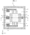
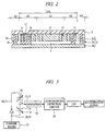
- Procédé de fabrication d'un dispositif pour système micro-électromécanique, comprenant les étapes consistant à :(a) préparer un substrat (2) qui inclut un élément de support (2a) et un conducteur (2c) prévu avec interposition d'un espace (4) entre le conducteur (2c) et l'élément de support (2a) ;(b) après l'étape (a), former un trou (18) dans le conducteur (2c) prévu au-dessus de l'espace (4), le trou (18) pénétrant le conducteur dans une direction de l'épaisseur du substrat (2) ;(c) après l'étape (b), prévoir un matériau de fixation (19) à travers le trou (18) à déposer sur l'élément de support (2a) et en outre remplir le trou (18) avec le matériau de fixation (19), en fixant de ce fait élément de support (2a) et le conducteur (2c) avec le matériau de fixation ; et(d) après l'étape (c), donner un motif au conducteur (2c), en formant de ce fait une portion de fixation (11) où l'élément de support (2a) et le conducteur (2c) sont fixés ensemble, un barreau (12) avec une extrémité connectée à la portion de fixation (11), et une portion mobile (13) connectée à l'autre extrémité du barreau (12).
- Procédé de fabrication d'un dispositif pour système micro-électromécanique selon la revendication 1,
dans lequel l'étape (a) inclut les sous-étapes consistant à :(a1) préparer un premier substrat pour être l'élément de support ;(a2) préparer un second substrat formé sur le conducteur ;(a3) former une portion concave au niveau d'une portion centrale du premier substrat ; et(a4) empiler le premier substrat et le second substrat, en formant ainsi l'espace défini par la portion concave entre le premier substrat et le second substrat. - Procédé de fabrication d'un dispositif pour système micro-électromécanique selon la revendication 2,
dans lequel le premier substrat est réalisé avec un matériau quelconque parmi du silicium, du verre et du métal,
le second substrat est réalisé avec un matériau quelconque parmi du silicium conducteur et du métal, et
dans l'étape (a4), le premier substrat et le second substrat sont réunis par un procédé d'union quelconque parmi l'union silicium-sur-silicium, l'union silicium-sur-métal, l'union silicium-sur-verre, l'union verre-sur-métal, et l'union métal-sur-métal. - Procédé de fabrication d'un dispositif pour système micro-électromécanique selon la revendication 1,
dans lequel l'étape (a) inclut les sous-étapes consistant à :(a1) après préparation d'un substrat de silicium ayant une première surface et une seconde surface opposée à la première surface, former une pluralité de tranchées sur l'une ou l'autre de la première surface et de la seconde surface ; et(a2) après l'étape (a1), exécuter un recuit à l'hydrogène du substrat de silicium, en reliant ainsi la pluralité de tranchées ensemble pour former l'espace, et former le substrat dans lequel l'élément de support et le conducteur sont formés du substrat de silicium. - Procédé de fabrication d'un dispositif pour système micro-électromécanique selon la revendication 1,
dans lequel l'étape (a) inclut les sous-étapes consistant à :(a1) après préparation d'un substrat de silicium ayant une première surface et seconde surface opposée à la première surface, former un film d'oxyde de silicium sur la première surface ;(a2) former un film de silicium polycristallin sur le film d'oxyde de silicium ;(a3) former une pluralité de tranchées dans le film de silicium polycristallin, la pluralité de tranchées atteignant le film d'oxyde de silicium ; et(a4) après l'étape (a3), exécuter un traitement à l'acide fluorhydrique sur le substrat de silicium, en supprimant ainsi le film d'oxyde de silicium au-dessous de la pluralité de tranchées pour former l'espace, et former le substrat dans lequel l'élément de support est formé du substrat de silicium et le conducteur est formé du film de silicium polycristallin. - Procédé de fabrication d'un dispositif pour système micro-électromécanique selon la revendication 1,
dans lequel, dans l'étape (c), le matériau de fixation est prévu à travers le trou pour être déposé sur l'élément de support, de manière à ne pas se projeter au-dessous du barreau adjacent à la portion de fixation. - Posséder de fabrication d'un dispositif pour système micro-électromécanique selon la revendication 1, dans lequel le conducteur (2c) comprend une première zone plane et une seconde zone plane en contact avec la première zone plane ; et
le trou (18) est formé dans le conducteur (2c) dans la seconde zone plane ; et
l'élément de support (2a) et le conducteur (2c) sont fixés dans la second zone plane avec le matériau de fixation ; et
la portion de fixation (11) du conducteur (2c) est formée dans la seconde zone plane et la portion mobile (13) et le barreau (12) du conducteur (2c) sont dans la première zone plane. - Procédé de fabrication d'un dispositif pour système micro-électromécanique selon la revendication 7,
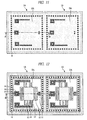
dans lequel le substrat comprend une troisième zone plane entourant la première zone plane et la seconde zone plane,
dans l'étape (b), un trou pénétrant dans une direction d'épaisseur du substrat est formé dans le conducteur dans la troisième zone plane,
dans l'étape (c), dans la troisième zone plane, le matériau de fixation est prévu à travers le trou pour être déposé sur l'élément de support, et la totalité est en outre remplie avec le matériau de fixation, en fixant ainsi l'élément de support et le conducteur dans la troisième zone plane avec le matériau de fixation,
dans l'étape (d), une base est formée depuis le conducteur dans la troisième zone plane, et
le procédé comprend encore, après l'étape (d), une étape (e) consistant à joindre un capuchon sur la base, le capuchon couvrant la première zone plane et la seconde zone plane. - Procédé de fabrication d'un dispositif pour système micro-électromécanique selon la revendication 7,
dans lequel le substrat comprend une troisième zone plane entourant la première zone plane et la seconde zone plane,
dans l'étape (b), des trous pénétrant dans une direction d'épaisseur du substrat sont formés à intervalles prédéterminés dans le conducteur dans la troisième zone plane,
dans l'étape (c), dans la troisième zone plane, le matériau de fixation est prévu à travers les trous de sorte que le matériel de fixation est déposé sur l'élément de support, et les trous sont en outre remplis avec le matériau de fixation, en formant ainsi une paroi dans l'espace, la paroi atteignant le conducteur depuis l'élément de support, et fixant l'élément de support et le conducteur dans la troisième zone plane avec le matériau de fixation,
dans l'étape (d), une base est formée depuis le conducteur dans la troisième zone plane, et
le procédé comprend encore, après l'étape (d), une étape (e) consistant à joindre un capuchon sur la base, le capuchon couvrant la première zone plane et la second zone plane, en scellant ainsi hermétiquement l'espace défini par le capuchon, l'élément de support et la paroi. - Procédé de fabrication d'un dispositif pour système micro-électromécanique selon la revendication 9,
dans lequel le conducteur est fait de silicium,
le capuchon est fait de verre, et dans l'étape (e), la base formée du conducteur et du capuchon sont fixés ensemble par une union silicium-sur-verre - Procédé de fabrication d'un dispositif pour système micro-électromécanique selon la revendication 9,
dans lequel le conducteur est fait de silicium,
le capuchon est fait de silicium, et
dans l'étape (e), la base formée du conducteur et du capuchon sont fixés ensemble par une union silicium-sur-silicium. - Procédé de fabrication d'un dispositif pour système micro-électromécanique selon la revendication 9,
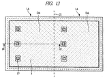
dans lequel une ouverture est formée dans le capuchon, et
après l'étape (c), un coussinet électrode est formé sur la portion de fixation, et dans l'étape (e), le coussinet électrode est exposé à travers l'ouverture.
Applications Claiming Priority (1)
| Application Number | Priority Date | Filing Date | Title |
|---|---|---|---|
| JP2007183159A JP4607153B2 (ja) | 2007-07-12 | 2007-07-12 | 微小電気機械システム素子の製造方法 |
Publications (3)
| Publication Number | Publication Date |
|---|---|
| EP2014612A2 EP2014612A2 (fr) | 2009-01-14 |
| EP2014612A3 EP2014612A3 (fr) | 2012-07-25 |
| EP2014612B1 true EP2014612B1 (fr) | 2013-12-18 |
Family
ID=39824950
Family Applications (1)
| Application Number | Title | Priority Date | Filing Date |
|---|---|---|---|
| EP08011540.5A Expired - Fee Related EP2014612B1 (fr) | 2007-07-12 | 2008-06-25 | Procédé de fabrication d'un dispositif micro-électromécanique évitant une couche sacrificielle |
Country Status (3)
| Country | Link |
|---|---|
| US (1) | US7972886B2 (fr) |
| EP (1) | EP2014612B1 (fr) |
| JP (1) | JP4607153B2 (fr) |
Families Citing this family (23)
| Publication number | Priority date | Publication date | Assignee | Title |
|---|---|---|---|---|
| US20110084356A1 (en) * | 2008-06-02 | 2011-04-14 | Nxp B.V. | Local buried layer forming method and semiconductor device having such a layer |
| JP5141490B2 (ja) * | 2008-10-08 | 2013-02-13 | ブラザー工業株式会社 | 光走査装置、画像形成装置、及び光走査装置の製造方法 |
| US8266962B2 (en) * | 2009-01-28 | 2012-09-18 | Infineon Technologies Ag | Acceleration sensor |
| JP5260342B2 (ja) * | 2009-01-30 | 2013-08-14 | ローム株式会社 | Memsセンサ |
| JP5444783B2 (ja) * | 2009-03-26 | 2014-03-19 | パナソニック株式会社 | 微小デバイス |
| JP2010251396A (ja) * | 2009-04-13 | 2010-11-04 | Toyota Central R&D Labs Inc | 可動部分と配線路を備えている装置 |
| JP2011048074A (ja) * | 2009-08-26 | 2011-03-10 | Seiko Epson Corp | 光偏向器の製造方法 |
| US8994128B2 (en) * | 2010-01-11 | 2015-03-31 | Elmos Semiconductor Ag | Micro-electromechanical semiconductor comprising stress measuring element and stiffening braces separating wall depressions |
| JP2011232447A (ja) * | 2010-04-26 | 2011-11-17 | Seiko Epson Corp | 光フィルター、光フィルターモジュール、および分析機器 |
| US8685778B2 (en) | 2010-06-25 | 2014-04-01 | International Business Machines Corporation | Planar cavity MEMS and related structures, methods of manufacture and design structures |
| EP2403139A1 (fr) * | 2010-07-02 | 2012-01-04 | Nxp B.V. | Résonateur |
| JP5419226B2 (ja) * | 2010-07-29 | 2014-02-19 | 日東電工株式会社 | フリップチップ型半導体裏面用フィルム及びその用途 |
| JP5492302B2 (ja) * | 2010-08-11 | 2014-05-14 | 日立オートモティブシステムズ株式会社 | 慣性センサ |
| EP2616389B1 (fr) * | 2010-09-18 | 2017-04-05 | Fairchild Semiconductor Corporation | Boîtier de microsystème électromécanique à puces multiples |
| JP5444199B2 (ja) * | 2010-12-06 | 2014-03-19 | 日立オートモティブシステムズ株式会社 | 複合センサ |
| US9139420B2 (en) * | 2012-04-18 | 2015-09-22 | Taiwan Semiconductor Manufacturing Company, Ltd. | MEMS device structure and methods of forming same |
| US9556016B2 (en) * | 2012-08-20 | 2017-01-31 | Robert Bosch Gmbh | Capacitive MEMS sensor and method |
| JP5688690B2 (ja) * | 2013-01-11 | 2015-03-25 | 横河電機株式会社 | 振動式トランスデューサおよび振動式トランスデューサの製造方法 |
| KR101738256B1 (ko) | 2015-09-09 | 2017-05-23 | 성균관대학교산학협력단 | 촉각 센서 |
| US9567208B1 (en) | 2015-11-06 | 2017-02-14 | Taiwan Semiconductor Manufacturing Company Ltd. | Semiconductor device and method for fabricating the same |
| JP2018179575A (ja) * | 2017-04-05 | 2018-11-15 | セイコーエプソン株式会社 | 物理量センサー、電子機器、および移動体 |
| JP2019060675A (ja) * | 2017-09-26 | 2019-04-18 | セイコーエプソン株式会社 | 物理量センサー、物理量センサー装置、電子機器、および移動体 |
| IT201900025084A1 (it) * | 2019-12-20 | 2021-06-20 | St Microelectronics Srl | Dispositivo microelettromeccanico dotato di una struttura orientabile protetta da urti |
Family Cites Families (16)
| Publication number | Priority date | Publication date | Assignee | Title |
|---|---|---|---|---|
| US5155061A (en) * | 1991-06-03 | 1992-10-13 | Allied-Signal Inc. | Method for fabricating a silicon pressure sensor incorporating silicon-on-insulator structures |
| FR2700003B1 (fr) * | 1992-12-28 | 1995-02-10 | Commissariat Energie Atomique | Procédé de fabrication d'un capteur de pression utilisant la technologie silicium sur isolant et capteur obtenu. |
| JPH10178181A (ja) | 1996-12-17 | 1998-06-30 | Mitsubishi Materials Corp | 半導体慣性センサの製造方法 |
| JP2000186931A (ja) * | 1998-12-21 | 2000-07-04 | Murata Mfg Co Ltd | 小型電子部品及びその製造方法並びに該小型電子部品に用いるビアホールの成形方法 |
| JP2001004658A (ja) | 1999-06-25 | 2001-01-12 | Matsushita Electric Works Ltd | 2軸半導体加速度センサおよびその製造方法 |
| JP4074051B2 (ja) | 1999-08-31 | 2008-04-09 | 株式会社東芝 | 半導体基板およびその製造方法 |
| JP4278960B2 (ja) * | 2002-08-08 | 2009-06-17 | 富士通コンポーネント株式会社 | マイクロリレー及びマイクロリレーの製造方法 |
| US6964882B2 (en) * | 2002-09-27 | 2005-11-15 | Analog Devices, Inc. | Fabricating complex micro-electromechanical systems using a flip bonding technique |
| US6933163B2 (en) * | 2002-09-27 | 2005-08-23 | Analog Devices, Inc. | Fabricating integrated micro-electromechanical systems using an intermediate electrode layer |
| TW570896B (en) | 2003-05-26 | 2004-01-11 | Prime View Int Co Ltd | A method for fabricating an interference display cell |
| JP2005165067A (ja) * | 2003-12-03 | 2005-06-23 | Seiko Epson Corp | 波長可変フィルタおよび波長可変フィルタの製造方法 |
| JP4210245B2 (ja) * | 2004-07-09 | 2009-01-14 | セイコーエプソン株式会社 | 波長可変フィルタ及び検出装置 |
| JP2006051549A (ja) * | 2004-08-09 | 2006-02-23 | Seiko Epson Corp | エッチング方法、振動子および電子機器 |
| JP5127181B2 (ja) * | 2005-08-10 | 2013-01-23 | 株式会社半導体エネルギー研究所 | 微小電気機械式装置の作製方法 |
| JP2008072209A (ja) * | 2006-09-12 | 2008-03-27 | Matsushita Electric Ind Co Ltd | 振動子、これをもちいた電気機械共振器及びその製造方法 |
| JP2008236386A (ja) * | 2007-03-20 | 2008-10-02 | Sony Corp | 電気機械素子とその製造方法、並びに共振器 |
-
2007
- 2007-07-12 JP JP2007183159A patent/JP4607153B2/ja not_active Expired - Fee Related
-
2008
- 2008-06-20 US US12/143,372 patent/US7972886B2/en not_active Expired - Fee Related
- 2008-06-25 EP EP08011540.5A patent/EP2014612B1/fr not_active Expired - Fee Related
Also Published As
| Publication number | Publication date |
|---|---|
| JP4607153B2 (ja) | 2011-01-05 |
| US7972886B2 (en) | 2011-07-05 |
| EP2014612A3 (fr) | 2012-07-25 |
| EP2014612A2 (fr) | 2009-01-14 |
| US20090017579A1 (en) | 2009-01-15 |
| JP2009018387A (ja) | 2009-01-29 |
Similar Documents
| Publication | Publication Date | Title |
|---|---|---|
| EP2014612B1 (fr) | Procédé de fabrication d'un dispositif micro-électromécanique évitant une couche sacrificielle | |
| CN106744649B (zh) | 具有两个掩埋腔的微机电器件及其制造方法 | |
| EP1920229B1 (fr) | Capteurs de pression et procedes de realisation | |
| US7998777B1 (en) | Method for fabricating a sensor | |
| EP1723072B1 (fr) | Suspension a support en pyramide | |
| US7662655B2 (en) | Vacuum packaged single crystal silicon device | |
| KR101437193B1 (ko) | 캡슐화 가능성을 갖는 마이크로미러 액튜에이터 및 그의 제조 방법 | |
| KR20170054258A (ko) | 차동 콤 드라이브 mems를 위한 시스템 및 방법 | |
| EP3052901B1 (fr) | Capteurs inertiels et de pression sur une seule puce | |
| EP0619471A1 (fr) | Procédé pour la fabrication d'un capteur de mouvement | |
| EP3241027B1 (fr) | Accéléromètre mems capacitif à trois axes sur substrat unique | |
| JP5048344B2 (ja) | 分離応力アイソレータ | |
| CN107529122B (zh) | 用于采收声能的mems装置及其制造方法 | |
| US6794271B2 (en) | Method for fabricating a microelectromechanical system (MEMS) device using a pre-patterned bridge | |
| JP2012122996A (ja) | Mems装置のためのウェハレベルパッケージプロセス | |
| KR20170004123A (ko) | 센서 소자 및 그 제조 방법 | |
| TWI815537B (zh) | 微機電裝置及其製造方法 | |
| US10524059B2 (en) | Capacitive-based transducer with high aspect ratio | |
| WO2002091439A1 (fr) | Fabrication de dispositif a systeme microelectromecanique | |
| Acar et al. | Fabrication Technologies |
Legal Events
| Date | Code | Title | Description |
|---|---|---|---|
| PUAI | Public reference made under article 153(3) epc to a published international application that has entered the european phase |
Free format text: ORIGINAL CODE: 0009012 |
|
| AK | Designated contracting states |
Kind code of ref document: A2 Designated state(s): AT BE BG CH CY CZ DE DK EE ES FI FR GB GR HR HU IE IS IT LI LT LU LV MC MT NL NO PL PT RO SE SI SK TR |
|
| AX | Request for extension of the european patent |
Extension state: AL BA MK RS |
|
| 17P | Request for examination filed |
Effective date: 20090409 |
|
| PUAL | Search report despatched |
Free format text: ORIGINAL CODE: 0009013 |
|
| AK | Designated contracting states |
Kind code of ref document: A3 Designated state(s): AT BE BG CH CY CZ DE DK EE ES FI FR GB GR HR HU IE IS IT LI LT LU LV MC MT NL NO PL PT RO SE SI SK TR |
|
| AX | Request for extension of the european patent |
Extension state: AL BA MK RS |
|
| RIC1 | Information provided on ipc code assigned before grant |
Ipc: B81C 1/00 20060101AFI20120620BHEP Ipc: G01P 15/125 20060101ALI20120620BHEP |
|
| 17Q | First examination report despatched |
Effective date: 20130117 |
|
| AKX | Designation fees paid |
Designated state(s): DE FR GB IT |
|
| RIC1 | Information provided on ipc code assigned before grant |
Ipc: G01P 15/08 20060101ALI20130404BHEP Ipc: G01P 15/125 20060101ALI20130404BHEP Ipc: B81C 1/00 20060101AFI20130404BHEP |
|
| GRAP | Despatch of communication of intention to grant a patent |
Free format text: ORIGINAL CODE: EPIDOSNIGR1 |
|
| GRAJ | Information related to disapproval of communication of intention to grant by the applicant or resumption of examination proceedings by the epo deleted |
Free format text: ORIGINAL CODE: EPIDOSDIGR1 |
|
| INTG | Intention to grant announced |
Effective date: 20130607 |
|
| GRAP | Despatch of communication of intention to grant a patent |
Free format text: ORIGINAL CODE: EPIDOSNIGR1 |
|
| INTG | Intention to grant announced |
Effective date: 20130705 |
|
| RAP1 | Party data changed (applicant data changed or rights of an application transferred) |
Owner name: HITACHI, LTD. |
|
| GRAS | Grant fee paid |
Free format text: ORIGINAL CODE: EPIDOSNIGR3 |
|
| GRAA | (expected) grant |
Free format text: ORIGINAL CODE: 0009210 |
|
| RIN1 | Information on inventor provided before grant (corrected) |
Inventor name: HANAOKA, YUKO, C/O HITACHI, LTD., INTELLECTUAL PRO Inventor name: JEONG, HEEWON, C/O HITACHI, LTD., INTELLECTUAL PRO Inventor name: FUJIMORI, TSUKASA, C/O HITACHI, LTD., INTELLECTUAL Inventor name: GOTO, YASUSHI, C/O HITACHI, LTD., INTELLECTUAL PRO |
|
| AK | Designated contracting states |
Kind code of ref document: B1 Designated state(s): DE FR GB IT |
|
| REG | Reference to a national code |
Ref country code: GB Ref legal event code: FG4D |
|
| REG | Reference to a national code |
Ref country code: DE Ref legal event code: R096 Ref document number: 602008029348 Country of ref document: DE Effective date: 20140213 |
|
| REG | Reference to a national code |
Ref country code: DE Ref legal event code: R097 Ref document number: 602008029348 Country of ref document: DE |
|
| PLBE | No opposition filed within time limit |
Free format text: ORIGINAL CODE: 0009261 |
|
| STAA | Information on the status of an ep patent application or granted ep patent |
Free format text: STATUS: NO OPPOSITION FILED WITHIN TIME LIMIT |
|
| 26N | No opposition filed |
Effective date: 20140919 |
|
| REG | Reference to a national code |
Ref country code: DE Ref legal event code: R097 Ref document number: 602008029348 Country of ref document: DE Effective date: 20140919 |
|
| REG | Reference to a national code |
Ref country code: FR Ref legal event code: PLFP Year of fee payment: 9 |
|
| REG | Reference to a national code |
Ref country code: FR Ref legal event code: PLFP Year of fee payment: 10 |
|
| PGFP | Annual fee paid to national office [announced via postgrant information from national office to epo] |
Ref country code: GB Payment date: 20170621 Year of fee payment: 10 Ref country code: FR Payment date: 20170511 Year of fee payment: 10 |
|
| PGFP | Annual fee paid to national office [announced via postgrant information from national office to epo] |
Ref country code: IT Payment date: 20170619 Year of fee payment: 10 |
|
| PGFP | Annual fee paid to national office [announced via postgrant information from national office to epo] |
Ref country code: DE Payment date: 20170621 Year of fee payment: 10 |
|
| REG | Reference to a national code |
Ref country code: DE Ref legal event code: R119 Ref document number: 602008029348 Country of ref document: DE |
|
| GBPC | Gb: european patent ceased through non-payment of renewal fee |
Effective date: 20180625 |
|
| PG25 | Lapsed in a contracting state [announced via postgrant information from national office to epo] |
Ref country code: GB Free format text: LAPSE BECAUSE OF NON-PAYMENT OF DUE FEES Effective date: 20180625 Ref country code: IT Free format text: LAPSE BECAUSE OF NON-PAYMENT OF DUE FEES Effective date: 20180625 Ref country code: FR Free format text: LAPSE BECAUSE OF NON-PAYMENT OF DUE FEES Effective date: 20180630 Ref country code: DE Free format text: LAPSE BECAUSE OF NON-PAYMENT OF DUE FEES Effective date: 20190101 |