EP2014612B1 - Method of manufacturing micro electro mechanical systems device avoiding a sacrificial layer - Google Patents
Method of manufacturing micro electro mechanical systems device avoiding a sacrificial layer Download PDFInfo
- Publication number
- EP2014612B1 EP2014612B1 EP08011540.5A EP08011540A EP2014612B1 EP 2014612 B1 EP2014612 B1 EP 2014612B1 EP 08011540 A EP08011540 A EP 08011540A EP 2014612 B1 EP2014612 B1 EP 2014612B1
- Authority
- EP
- European Patent Office
- Prior art keywords
- substrate
- conductor
- silicon
- planar area
- supporting member
- Prior art date
- Legal status (The legal status is an assumption and is not a legal conclusion. Google has not performed a legal analysis and makes no representation as to the accuracy of the status listed.)
- Expired - Fee Related
Links
Images


Classifications
-
- B—PERFORMING OPERATIONS; TRANSPORTING
- B81—MICROSTRUCTURAL TECHNOLOGY
- B81C—PROCESSES OR APPARATUS SPECIALLY ADAPTED FOR THE MANUFACTURE OR TREATMENT OF MICROSTRUCTURAL DEVICES OR SYSTEMS
- B81C1/00—Manufacture or treatment of devices or systems in or on a substrate
- B81C1/00912—Treatments or methods for avoiding stiction of flexible or moving parts of MEMS
- B81C1/0092—For avoiding stiction during the manufacturing process of the device, e.g. during wet etching
- B81C1/00952—Treatments or methods for avoiding stiction during the manufacturing process not provided for in groups B81C1/00928 - B81C1/00944
-
- B—PERFORMING OPERATIONS; TRANSPORTING
- B81—MICROSTRUCTURAL TECHNOLOGY
- B81C—PROCESSES OR APPARATUS SPECIALLY ADAPTED FOR THE MANUFACTURE OR TREATMENT OF MICROSTRUCTURAL DEVICES OR SYSTEMS
- B81C1/00—Manufacture or treatment of devices or systems in or on a substrate
- B81C1/00015—Manufacture or treatment of devices or systems in or on a substrate for manufacturing microsystems
- B81C1/00023—Manufacture or treatment of devices or systems in or on a substrate for manufacturing microsystems without movable or flexible elements
- B81C1/00039—Anchors
-
- G—PHYSICS
- G01—MEASURING; TESTING
- G01C—MEASURING DISTANCES, LEVELS OR BEARINGS; SURVEYING; NAVIGATION; GYROSCOPIC INSTRUMENTS; PHOTOGRAMMETRY OR VIDEOGRAMMETRY
- G01C19/00—Gyroscopes; Turn-sensitive devices using vibrating masses; Turn-sensitive devices without moving masses; Measuring angular rate using gyroscopic effects
- G01C19/56—Turn-sensitive devices using vibrating masses, e.g. vibratory angular rate sensors based on Coriolis forces
- G01C19/5719—Turn-sensitive devices using vibrating masses, e.g. vibratory angular rate sensors based on Coriolis forces using planar vibrating masses driven in a translation vibration along an axis
- G01C19/5733—Structural details or topology
- G01C19/5755—Structural details or topology the devices having a single sensing mass
-
- G—PHYSICS
- G01—MEASURING; TESTING
- G01P—MEASURING LINEAR OR ANGULAR SPEED, ACCELERATION, DECELERATION, OR SHOCK; INDICATING PRESENCE, ABSENCE, OR DIRECTION, OF MOVEMENT
- G01P15/00—Measuring acceleration; Measuring deceleration; Measuring shock, i.e. sudden change of acceleration
- G01P15/02—Measuring acceleration; Measuring deceleration; Measuring shock, i.e. sudden change of acceleration by making use of inertia forces using solid seismic masses
- G01P15/08—Measuring acceleration; Measuring deceleration; Measuring shock, i.e. sudden change of acceleration by making use of inertia forces using solid seismic masses with conversion into electric or magnetic values
- G01P15/0802—Details
-
- G—PHYSICS
- G01—MEASURING; TESTING
- G01P—MEASURING LINEAR OR ANGULAR SPEED, ACCELERATION, DECELERATION, OR SHOCK; INDICATING PRESENCE, ABSENCE, OR DIRECTION, OF MOVEMENT
- G01P15/00—Measuring acceleration; Measuring deceleration; Measuring shock, i.e. sudden change of acceleration
- G01P15/02—Measuring acceleration; Measuring deceleration; Measuring shock, i.e. sudden change of acceleration by making use of inertia forces using solid seismic masses
- G01P15/08—Measuring acceleration; Measuring deceleration; Measuring shock, i.e. sudden change of acceleration by making use of inertia forces using solid seismic masses with conversion into electric or magnetic values
- G01P15/125—Measuring acceleration; Measuring deceleration; Measuring shock, i.e. sudden change of acceleration by making use of inertia forces using solid seismic masses with conversion into electric or magnetic values by capacitive pick-up
-
- B—PERFORMING OPERATIONS; TRANSPORTING
- B81—MICROSTRUCTURAL TECHNOLOGY
- B81B—MICROSTRUCTURAL DEVICES OR SYSTEMS, e.g. MICROMECHANICAL DEVICES
- B81B2201/00—Specific applications of microelectromechanical systems
- B81B2201/02—Sensors
- B81B2201/0228—Inertial sensors
- B81B2201/0235—Accelerometers
-
- B—PERFORMING OPERATIONS; TRANSPORTING
- B81—MICROSTRUCTURAL TECHNOLOGY
- B81B—MICROSTRUCTURAL DEVICES OR SYSTEMS, e.g. MICROMECHANICAL DEVICES
- B81B2203/00—Basic microelectromechanical structures
- B81B2203/03—Static structures
- B81B2203/0307—Anchors
-
- B—PERFORMING OPERATIONS; TRANSPORTING
- B81—MICROSTRUCTURAL TECHNOLOGY
- B81C—PROCESSES OR APPARATUS SPECIALLY ADAPTED FOR THE MANUFACTURE OR TREATMENT OF MICROSTRUCTURAL DEVICES OR SYSTEMS
- B81C2201/00—Manufacture or treatment of microstructural devices or systems
- B81C2201/01—Manufacture or treatment of microstructural devices or systems in or on a substrate
- B81C2201/0174—Manufacture or treatment of microstructural devices or systems in or on a substrate for making multi-layered devices, film deposition or growing
- B81C2201/019—Bonding or gluing multiple substrate layers
-
- B—PERFORMING OPERATIONS; TRANSPORTING
- B81—MICROSTRUCTURAL TECHNOLOGY
- B81C—PROCESSES OR APPARATUS SPECIALLY ADAPTED FOR THE MANUFACTURE OR TREATMENT OF MICROSTRUCTURAL DEVICES OR SYSTEMS
- B81C2203/00—Forming microstructural systems
- B81C2203/05—Aligning components to be assembled
- B81C2203/058—Aligning components using methods not provided for in B81C2203/051 - B81C2203/052
Definitions
- the present invention relates to a technology for manufacturing a Micro Electro Mechanical Systems (MEMS) device having a movable portion or a suspension portion such as an acceleration sensor, an angular velocity sensor, a resonator, a mechanical filter, or a micromirror.
- MEMS Micro Electro Mechanical Systems
- it relates to a technology for manufacturing a hermetically-sealed MEMS device which exchanges electric signals with the outside.
- a MEMS device having a supporting member formed of a silicon substrate, a fixing portion formed on the supporting member, and a flat plate-shaped movable portion provided with interposing a space between the movable portion and the supporting member, in which the fixing portion supports the movable portion via a beam, has been suggested.
- This MEMS device detects a displacement of the movable portion as a change of a capacitance value.
- the space of the MEMS device is formed by removing a sacrificial layer provided between the supporting member and the movable portion and beam, and a cavity in a cavity layer formed by the removal corresponds to the space.
- a sticking phenomenon in which the beam comes into contact with the supporting member occurs in some cases.
- Patent Document 1 a silicon wafer (silicon substrate) having a concave portion formed thereon is first attached onto a glass substrate serving as a supporting member, thereby forming a cavity layer.
- the silicon wafer is subjected to anisotropic etching to form functional portions such as a fixing portion, a beam, and a movable portion. Therefore, since the etching of a sacrificial layer is not required, the occurrence of the sticking phenomenon can be reduced.
- a concave portion is first formed on a glass substrate. Then, a silicon wafer (silicon substrate) having an oxide film on one surface thereof and a nickel film to be used as a mask in silicon etching on the other surface thereof is fabricated. Thereafter, the nickel mask is patterned and the silicon wafer is subjected to anisotropic etching with using the nickel film as a mask, thereby forming a movable portion. At this time, the oxide film formed on the opposite surface is used as an etch stop layer.
- the nickel layer used as the mask is removed from the silicon wafer, and then the silicon wafer is anodically-bonded to the glass substrate. Thereafter, the oxide film on the surface of the silicon wafer is removed.
- an SON (Silicon On Nothing) wafer (SON substrate) is used.
- the SON wafer can be formed by bonding a flat wafer (glass substrate) onto one silicon wafer (silicon substrate) having a concave portion formed thereon.
- the SON wafer can be fabricated by the manufacturing methods introduced in Applied Physics Letters, Vol. 77, No. 20, 2000, pp. 3290-3292 (Non-Patent Document 1) and Journal of Vacuum Science and Technology A 18(4), 2000, pp. 1853-1858 (Non-Patent Document 2).
- the Non-Patent Document 1 introduces a process of forming a space (cavity) by deeply digging a micro-hole on the order of sub-microns in the surface of a silicon wafer and then performing hydrogen-annealing. Also, although the Non-Patent Document 2 does not describe a method of manufacturing a SON wafer, it describes a process that can be applied to the SON manufacture as it is.
- a cavity layer is formed in advance in a silicon wafer, and the anisotropic etching is performed from the rear surface of a cavity-layer formation surface. Therefore, when forming the cavity layer, it is required to form an island-shaped bank portion in advance at a position corresponding to a fixing portion formed in a latter process, and double-side processing of the silicon wafer is inevitable.
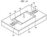
- FIG. 14 A MEMS device using such a technology as described in the Patent Document 2 studied by the inventors of the present invention is shown in FIG. 14 .
- a reference numeral 100 denotes a supporting member
- 101 denotes a fixing portion
- 102 denotes a bank portion
- 103 denotes a movable portion
- 104 denotes a cavity layer
- 105 denotes a beam, respectively.
- the bank portions 102 In order to bond a silicon wafer which has been subjected to anisotropic etching onto the supporting member 100 having a concave portion formed thereon and to suspend the movable portion 103 formed on the silicon wafer, the bank portions 102 have to be formed on the supporting member 10 side, and the size thereof has to be determined in consideration of an error in alignment.
- a large angle error in alignment sometimes causes a misalignment between the bank portion 102 formed on the supporting member 100 and the fixing portion 101 formed on the silicon wafer.
- the length of the fixing portion 101 to be bonded onto the supporting member 100 and the length of the beam 105 connecting this fixing portion 101 and the movable portion 103 do not match in some cases. In this case, deterioration in performance such as deterioration in resonance frequency of the sensor and occurrence of unwanted mode may occur.
- manufacturing yield is deteriorated.
- the silicon wafer to which anisotropic processing has been completed is bonded onto the supporting member formed of a glass substrate, breakage of the movable portion occurs at the time of bonding.
- the oxide film formed on the front surface is removed with etchant after the bonding, in a sensor having a small-sized movable toothed gear or fixing pattern such as a fixed toothed gear, the movable portion may possibly be stuck to the surrounding fixed pattern (in particular, the movable toothed gear and the fixed toothed pattern together).
- An object of the present invention is to provide a MEMS device which is robust to the misalignment and does not require the double-side wafer processing in the manufacture of a MEMS device such as an angular velocity sensor, an acceleration sensor, a combined sensor (sensor in which an angular velocity sensor and an acceleration sensor are integrated together), or a micromirror.
- a substrate that includes a supporting member and a conductor provided with interposing a space between the conductor and the supporting member and that has a first planar area and a second planar area in contact with the first planar area is prepared. Then, (b) a hole penetrating in a thickness direction of the substrate is formed in the conductor in the second planar area. Then, (c) a fixing material is provided through the hole to be deposited on the supporting member and further the hole is filled with the fixing material, thereby fixing the supporting member and the conductor in the second planar area with the fixing material.
- the conductor is patterned, thereby forming a fixing portion from the conductor in the second planar area and forming a movable portion and a beam, which connects the movable portion and the fixing portion, from the conductor in the first planar area.
- a substrate having a space formed therein is used, micro-holes are formed at necessary portions, and the holes are filled with a fixing material to fix surrounding portions of the holes to the supporting member. Therefore, different from the technology described in the Patent Document 1, the double-side processing for the wafer is not required. Also, since it is not required to know in advance the position where the fixing portion is to be placed when forming the space, a large amount of standard substrates (wafers) having a space can be produced. Furthermore, since a movable portion and a fixing portion are formed after the substrate (wafer) formed of a conductor and the substrate (wafer) to be a supporting member are bonded together, highly accurate alignment is not required. As a result, high-performance and highly reliable MEMS devices with little individual difference between devices can be manufactured.
- the number of the elements is not limited to a specific number unless otherwise stated or except the case where the number is apparently limited to a specific number in principle, and the number larger or smaller than the specified number is also applicable.
- a Micro Electro Mechanical Systems device (hereinafter, referred to as a MEMS device) according to a present embodiment will be described with reference to the drawings.
- a MEMS device A Micro Electro Mechanical Systems device (hereinafter, referred to as a MEMS device) according to a present embodiment will be described with reference to the drawings.
- an acceleration sensor is taken as an example of the MEMS device.
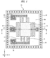
- FIG. 1 is a plan view of main components of the acceleration sensor according to the present embodiment.
- FIG. 2 is a cross-sectional view of the acceleration sensor taken along the line A-A' in FIG. 1 .
- a substrate 2 having a space 4 is used for the acceleration senor 1A.
- a space layer 2b is formed by forming a concave portion (space 4) on a supporting substrate 2a of a supporting member by the use of photolithography and etching, and then a device layer 2c formed of a conductor is bonded thereto. After the bonding, the thickness of the device layer 2c is adjusted by polishing or dry etching using plasma.
- a layer having the space 4 and placed on the supporting substrate 2a constituting a substrate 2 is taken as the space layer 2b.
- a layer on which main components of the acceleration sensor 1A are formed and placed on the space layer 2b is taken as the device layer 2c.
- the space layer 2b is formed on the supporting substrate 2a
- the device layer 2c is formed on the space layer 2b.
- FIG. 2 shows an area A1 included in the device formation area DA and having a movable portion 13 formed therein and an area A2 in contact with the area A1 and having components such as a fixing portion 11 and a terminal portion 16 fixed to the supporting substrate 2a formed therein. Further, FIG. 2 also shows an area A3 surrounding the device formation area DA and having the base 10 formed therein.
- the supporting substrate 2a is formed of, for example, a silicon (Si) substrate
- the device layer 2c is formed of, for example, a conductive silicon substrate.
- the supporting substrate 2a has a thickness of, for example, several tens to several hundreds ⁇ m
- the space layer 2b has a thickness of, for example, several hundreds nm to several ⁇ m
- the device layer 2c has a thickness of, for example, several hundreds nm to several tens ⁇ m.
- a silicon substrate semiconductor substrate
- conductive polysilicon using surface MEMS technology or plated metal such as nickel (Ni) may be used for the device layer 2c.
- components fixed to the supporting substrate 2a such as the base 10 are adhered and fixed to the supporting substrate 2a by filling the holes 18 formed in advance with a fixing material 19 so that the fixing material 19 reaches the supporting substrate 2a.
- the fixing portion 11 is formed by patterning the device layer 2c.
- This fixing portion 11 is fixed to the supporting substrate 2a via the fixing material 19 in the space layer 2b.
- a beam 12 supporting the movable portion 13 to be described later is connected to this fixing portion 11.
- the movable portion 13 is formed by patterning the device layer 2c. Since this movable portion 13 is supported by the beam 12 and the space 4 is formed below the movable portion 13, the movable portion 13 is separated from the supporting substrate 2a and is suspended on the fixing portion 11.
- a movable electrode 14 Since a movable electrode 14 is fixed (connected) to only the movable portion 13, it moves in the same manner as that of the movable portion 13.
- the fixed electrode 15 is disposed so as to face the movable electrode 14 and is fixed to the supporting substrate 2a via the fixing material 19 of the space layer 2b.
- a capacitance is formed between the fixed electrode 15 and the movable electrode 14. When acceleration is applied to displace the movable portion 13 and the movable electrodes 14, the capacitance is also changed.
- a detection circuit for detecting the change will be described further below with reference to FIG. 3 .
- the terminal portion 16 is connected to the fixed electrode 15 and is fixed to the supporting substrate 2a via the fixing material 19 of the space layer 2b. Also, an electrode pad 17 formed of a metal film made of Al is formed on the terminal portion 16, and electric signals are exchanged with the outside.
- fixed components formed on the device layer 2c such as the base 10, the fixing portion 11, the fixed electrodes 15 and the terminal portion 16 are fixed to the supporting substrate 2a via the underlying space layer 2b by filling the holes 18 formed in advance with the fixing material 19 so that the fixing material 19 reaches the supporting substrate 2a.
- movable components such as the beam 12, the movable portion 13 and the movable electrodes 14 are in a state of being suspended on the fixing portion 11 because the space 4 is formed therebelow.
- the movable components are configured to move within a plane of the device layer 2c parallel to a main surface of the substrate 2 having the space 4.
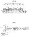
- a cap 3 is bonded onto the base 10, and this cap 3 is disposed so as to cover the device formation area DA of the acceleration sensor 1A.
- This cap 3 is formed of, for example, a glass substrate and is bonded onto the base 10 made of silicon by anodic bonding. Furthermore, an opening is formed in this cap 3 at the position to which the electrode pad 17 is bonded, and electrical signals can be exchanged with the outside of the device by such means as wire bonding.
- one feature of the present invention lies in a method of fixing such fixed components as the base 10, the fixing portion 11, the fixed electrodes 15 and the terminal portion 16 by the use of the substrate 2 having the space 4.
- the holes 18 are formed in these components in advance, and by filling the holes 18 with the fixing material 19 so that the fixing material 19 reaches the supporting substrate 2a, the fixed components are adhered to the supporting substrate 2a via the space layer 2b. More specifically, since the portions where the holes 18 are formed are fixed, at the time of manufacturing the wafer (disk-shaped substrate 2) having the space 4, no particular consideration is required for a position of a pattern to be formed later. Therefore, as studied by the inventors of the present invention, the double-side processing on the wafer and the highly accurate bonding alignment are not required.
- the space layer 2b is present below the device layer 2c where sensor components such as the movable portion 13 and the beam 12 are formed, for example, the movable portion 13 can be released only by patterning the device layer 2c. Therefore, it becomes unnecessary to perform an etch-hole forming process for floating the movable portion and a releasing process for removing the insulator below the movable portion, which are indispensable in the manufacturing method using a Silicon On Insulation (SOI) substrate in which an insulating layer is present between the device layer 2c and the supporting substrate 2a. Accordingly, the mass per unit area can be increased, and the downsizing and the performance improvement of the sensor can be achieved.
- SOI Silicon On Insulation
- the fixing portion 11 is fixed to the supporting substrate 2a via the space layer 2b by filling the holes 18 with the fixing material 19 so that the fixing material 19 reaches the supporting substrate 2a. Thereafter, the device layer 2c formed around the holes 18 is patterned to form the fixing portion 11. Therefore, the fixing material 19 which is formed below the fixing portion 11 and fixes the fixing portion 11 to the supporting substrate 2a via the space layer 2b is inevitably formed inside the fixing portion 11, and it does not protrude from (reach) the fixing portion 11. In other words, the fixing material 19 is provided through the holes 18 to be deposited on the supporting substrate 2a so as not to protrude below the beam 12 adjacent to the fixing portion 11.
- the beam 12 connected to the fixing portion 11 to support the movable portion 13 can be formed to have dimensions as designed without requiring highly-accurate alignment.
- high-performance sensors with less deviation in resonance frequency and less occurrence of unwanted mode can be achieved and individual difference between devices can be reduced.
- high-performance acceleration sensors can be achieved with high yield.
- the movable portion 13 and the movable electrodes 14 are connected to the beam 12 that is easily displaced in an x direction but hardly displaced in a y direction.
- x m / k ⁇ a
- FIG. 3 shows a detection circuit for extracting an acceleration signal from the capacitance change.
- the movable electrode 14 and the fixed electrode 15 are represented as capacitors, and the beam 12, the movable portion 13, the movable electrode 14, the fixed electrode 15, the terminal portion 16 and the electrode pad 17 are represented as wirings.
- the same reference numerals are provided as an equivalent circuit in FIG. 3 .
- Carrier waves 51 that differ in phase by 180 degrees are applied to each of the fixed electrodes 15, and a difference therebetween is amplified by an amplifier 52 and is then subjected to synchronous detection by a synchronous detection circuit 53, thereby outputting a voltage signal proportional to the applied acceleration. Further, it has been known that an electrode that cancels out the force F generated by the applied acceleration by means of a re-balance force generated by an electrostatic force is provided to the movable portion 13 and a voltage to be applied to this electrode is monitored, thereby detecting the applied acceleration.
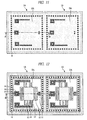
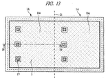
- FIG. 4 is a cross-sectional view of a substrate having a space in a wafer state during a manufacturing process.
- FIG. 5 to FIG. 10 are cross-sectional views of main parts of the MEMS device during the manufacturing process.
- FIG. 11 to FIG. 13 are plan views of the main parts of the MEMS device during the manufacturing process. Note that FIG. 5 to FIG. 10 show the cross sections taken along the line B-B' in FIG. 11 to FIG. 13 .
- the substrate 2 having the supporting substrate 2a to be a supporting member and the device layer 2c formed of a conductor provided with interposing the space 4 (space layer 2b) between the supporting substrate 2a and the device layer 2c is prepared. Specifically, a first silicon substrate constituting the supporting substrate 2a and a conductive second silicon substrate constituting the device layer 2c are prepared. Note that, though not shown in FIG. 4 , as described with reference to FIG.
- the substrate 2 has the area A1 included in the device formation area DA and having the movable portion 13 formed therein, the area A2 in contact with the area A1 and having components such as the fixing portion 11 and the terminal portion 16 fixed to the supporting substrate 2a formed therein, and the area A3 surrounding the device formation area DA and having the base 10 formed therein.
- a concave portion is formed at a center portion of the supporting substrate 2a by using photolithography and etching, and then the first silicon substrate and the second silicon substrate are stacked and bonded to each other by normal-temperature bonding method.
- the space 4 constituted of the concave portion is formed between the supporting substrate 2a formed of the first silicon substrate and the device layer 2c formed of the second silicon substrate.
- the thickness of the device layer 2c is adjusted by polishing or dry etching using SF 6 gas. In this manner, the substrate 2 having the space layer 2b in which the space 4 is formed between the silicon substrates can be prepared.
- the first silicon substrate for use as the supporting substrate 2a is also used as a simple supporting substrate, it is not necessarily made of silicon, but a glass or metal plate may be used.
- the second silicon substrate for use as the device layer 2c is not particularly limited as long as it is a conductive film such as a metal plate.
- the supporting member to be the supporting substrate 2a may be made of silicon, glass or metal, and the conductor constituting the device layer 2c may be made of conductive silicon or metal.
- the conductor and the supporting member are stacked and bonded to each other by silicon-silicon bonding, silicon-metal bonding, silicon-glass bonding, glass-metal bonding or metal-metal bonding, thereby forming the substrate 2 having the space 4.
- the processes of forming the holes 18, filling the fixing material 19 and forming the electrode pad 17 will be described.
- the micro-holes 18 penetrating in a thickness direction of the substrate 2 are formed in the areas A2 and A3 of the device layer 2c.
- These holes 18 are filled with the fixing material 19, so that fixed components such as the base 10, the fixing portion 11, the fixed electrodes 15, and the terminal portion 16 that are formed in latter processes are fixed to the supporting substrate 2a via the space layer 2b. Therefore, the holes 18 are formed so as to penetrate through the device layer 2c in accordance with the shape and position of each component to be fixed to the supporting substrate 2a such as the base 10 and the fixing portion 11.
- the diameter of each hole 18 is preferably equal to or twice as large as the thickness of the space layer 2b.
- the fixing material 19 is provided through the holes 18 to be deposited on the supporting substrate 2a. Furthermore, the holes 18 are filled with the fixing material 19, thereby fixing the supporting substrate 2a and the device layer 2c in the areas A2 and A3 with the fixing material 19. Specifically, the holes 18 are filled with the fixing material 19 by using a film formation method such as Chemical Vapor Deposition (CVD), and a portion of the device layer 2c surrounding a portion where the holes 18 are formed is fixed to the supporting substrate 2a.
- CVD Chemical Vapor Deposition
- a wall of the fixing material 19 between the device layer 2c and the supporting substrate 2a by appropriately considering the shape, interval and size of each hole 18.
- a film of the fixing material 19 formed below the base 10 has not only the function to fix the base 10 to the supporting substrate 2a but also the function to form a hermetic device formation area DA (refer to FIG. 2 ) by forming a wall between the device layer 2c and the supporting substrate 2a.
- CMP Chemical Mechanical Polishing
- the electrode pad 17 is formed by patterning the metal conductive film by using photolithography and etching.
- the device layer 2c is patterned by using photolithography and etching, thereby forming the base 10 in which the supporting substrate 2a and the device layer 2c in the area A3 are fixed together. Also, the fixing portion 11 and the terminal portion 16 in which the supporting substrate 2a and the device layer 2c in the area A2 are fixed together and the beam 12 with one end connected to the fixing portion 11 are formed in the same manner. Furthermore, the movable portion 13 connected to the other end of the beam 12 is formed from the device layer 2c in the area A1.
- the base 10 is formed in a closed-curve shape in the device layer 2c so as to surround the device formation area DA. Since the cap 3 formed in a latter process is bonded to the base 10 to form a hermetically-sealed space (device formation area DA), the base 10 has to be firmly adhered to the supporting substrate 2a, and the space layer 2b below the base 10 has to be filled. For this purpose, the holes 18 are densely formed in this base 10, and the fixing material 19 is formed in the space layer 2b below the base 10 so as to be a wall. The base 10 is formed by etching the portion around these holes 18 into a band shape so as to penetrate through the device layer 2c.
- the fixing portion 11 is a portion fixed to the supporting substrate 2a to suspend the movable portion 13 on the beam 12 or the like formed together. Similar to the base 10, the fixing portion 11 is fixed by filling the holes 18 formed in advance with the fixing material 19 so that the fixing material 19 reaches the supporting substrate 2a. The fixing portion 11 is formed by removing the device layer 2c around these holes 18 by etching.
- the beam 12 is formed by removing the device layer 2c around the beam 12 by etching. This beam 12 is connected to the fixing portion 11 and movably supports the movable portion 13 and the movable electrodes 14.
- the movable portion 13 is formed by removing the surrounding device layer 2c by etching. This movable portion 13 is connected to the beam 12, works as the mass of the acceleration sensor 1A, and is displaced in proportion to the acceleration when applied.
- the fixing portion 11, the beam 12 and the movable portion 13, the movable electrodes 14 are formed by removing the surrounding device layer 2c by etching. These movable electrodes 14 are connected to the movable portion 13 and move in the same manner as that of the movable portion 13.
- the fixing portion 11, the beam 12, the movable portion 13 and the movable electrodes 14, the fixed electrodes 15 are formed by removing the surrounding device layer 2c by etching. Similar to the base 10 and the fixing portion 11, these fixed electrodes 15 are fixed by filling the holes 18 formed in advance with the fixing material 19 so that the fixing material 19 reaches the supporting substrate 2a.
- the terminal portion 16 is formed by removing the surrounding device layer 2c by etching. Similar to the base 10, the fixing portion 11 and the fixed electrodes 15, the terminal portion 16 is fixed by filling the holes 18 formed in advance with the fixing material 19 so that the fixing material 19 reaches the supporting substrate 2a. Also, the terminal portion 16 is connected to the fixed electrodes 15, and the electrode pad 17 is formed in advance on the terminal portion 16.
- the cap 3 having openings formed in advance is bonded onto the base 10, and the electrode pads 17 are exposed through these openings.
- This cap 3 is formed so as to cover the device formation area DA, and the device formation area DA in which the structure of the acceleration sensor is formed is hermetically sealed with the cap 3. Also, the hermetically-sealed movable electrodes 14 and fixed electrodes 15 are electrically connected to the outside via the electrode pad 17. Therefore, it is possible to exchange electric signals with the outside.
- a glass substrate is used as the cap 3.
- another substrate made of different insulator such as an insulating silicon substrate may be used.
- the cap 3 and the base 10 may be bonded with normal-temperature bonding using the surface activation by plasma or ions or may be bonded with an adhesive such as glass frit or solder.
- the cap 3 and the base 10 can be bonded with normal-temperature bonding.
- the cap 3 and the base 10 are made of the same material, sealing distortion due to a difference in a temperature coefficient of expansion between sealing materials can be eliminated, and thus a high-performance angular velocity detection device can be obtained.
- the substrate 2 bonded to the cap 3 is diced along a dicing line 21, thereby obtaining the pieces of the acceleration sensor 1A.
- the acceleration sensor 1A according to the present embodiment can be formed.
- an acceleration sensor is described as an example of the MEMS device.
- the gist of the present invention is not restricted to the acceleration sensor, but is directed to a technology effective in a structure such as an angular velocity sensor or a resonator, in which the structure of the device layer 2c is suspended on the supporting substrate 2a.
- a smooth and large area to be a mirror can be released without forming etch holes.
- a silicon wafer silicon substrate
- a plurality of trenches (holes) on the order of sub-microns are formed on a front surface or rear surface side.
- the silicon substrate is subjected to hydrogen-annealing to link the plurality of trenches together, thereby forming the space 4.
- the substrate 2 in which the supporting substrate 2a (supporting member) and the device layer 2c (conductor) are formed of the silicon substrate can be formed.
- a silicon wafer silicon substrate
- a silicon oxide film is formed on the front surface
- a conductive polycrystalline silicon film is formed on the silicon oxide film.
- the silicon substrate is subjected to hydrofluoric acid treatment, thereby removing the silicon oxide film below the plurality of trenches to form the space 4.
- the substrate 2 in which the supporting substrate 2a (supporting member) is formed of the silicon substrate and the device layer 2c (conductor) is formed of the conductive polycrystalline silicon film can be formed.
- the structure of the substrate 2 shown in FIG. 1 and FIG. 2 can be formed in the following manner. First, a first silicon substrate to be the supporting substrate 2a (supporting member) and a conductive second silicon substrate constituting the device layer 2c (conductor) are prepared. Next, a convex portion is formed on the first silicon substrate. This convex portion corresponds to the wall formed of the fixing material 19 in the space layer 2b described above, and is formed of the first silicon substrate. Next, by the use of the normal-temperature bonding method, the first silicon substrate and the second silicon substrate are fixed together at the convex portion, thereby forming the space 4 between the first silicon substrate and the second silicon substrate.
- the holes 18 in the device layer 2c described above are not formed, and the device layer 2c is formed of the second silicon substrate.
- the device layer 2c is patterned, thereby forming a fixing portion where the first silicon substrate and the second silicon substrate are fixed together, a beam with one end connected to the fixing portion, and a movable portion connected to the other end of the beam.
- the structure of the substrate 2 shown in FIG. 1 and FIG. 2 is completed.
- the supporting substrate 2a may be made of not only silicon but also glass or metal
- the device layer 2c may be made of not only conductive silicon but also metal.
- the present invention can be applied to an inertial-force detection sensor such as an angular velocity sensor and vibrating MEMS devices such as a resonator, a mechanical filter and a micromirror.
- the present invention can be widely used for the manufacturing industry of MEMS devices.
Landscapes
- Engineering & Computer Science (AREA)
- Physics & Mathematics (AREA)
- General Physics & Mathematics (AREA)
- Manufacturing & Machinery (AREA)
- Microelectronics & Electronic Packaging (AREA)
- Radar, Positioning & Navigation (AREA)
- Remote Sensing (AREA)
- Chemical & Material Sciences (AREA)
- Analytical Chemistry (AREA)
- Pressure Sensors (AREA)
- Micromachines (AREA)
Abstract
Description
- The present invention relates to a technology for manufacturing a Micro Electro Mechanical Systems (MEMS) device having a movable portion or a suspension portion such as an acceleration sensor, an angular velocity sensor, a resonator, a mechanical filter, or a micromirror. In particular, it relates to a technology for manufacturing a hermetically-sealed MEMS device which exchanges electric signals with the outside.
- For example, a MEMS device having a supporting member formed of a silicon substrate, a fixing portion formed on the supporting member, and a flat plate-shaped movable portion provided with interposing a space between the movable portion and the supporting member, in which the fixing portion supports the movable portion via a beam, has been suggested. This MEMS device detects a displacement of the movable portion as a change of a capacitance value.
- In the method of forming the MEMS device, the space of the MEMS device is formed by removing a sacrificial layer provided between the supporting member and the movable portion and beam, and a cavity in a cavity layer formed by the removal corresponds to the space. However, in the course of the manufacturing process or during use of the product, a sticking phenomenon in which the beam comes into contact with the supporting member occurs in some cases. Thus, in the semiconductor sensor and the manufacturing method thereof already known to the public based on the specification of Japanese Patent Application Laid-Open Publication No.
2001-4658 - Also, in the method of manufacturing a MEMS device already known to the public based on the specification of Japanese Patent Application Laid-Open Publication No.
10-178181 - Note that, in the MEMS device, as introduced in the
Patent Documents 1 and 2, an SON (Silicon On Nothing) wafer (SON substrate) is used. As an example of the manufacturing method thereof, the SON wafer can be formed by bonding a flat wafer (glass substrate) onto one silicon wafer (silicon substrate) having a concave portion formed thereon. Further, other than these methods, the SON wafer can be fabricated by the manufacturing methods introduced in Applied Physics Letters, Vol. 77, No. 20, 2000, pp. 3290-3292 (Non-Patent Document 1) and Journal of Vacuum Science and Technology A 18(4), 2000, pp. 1853-1858 (Non-Patent Document 2). The Non-Patent Document 1 introduces a process of forming a space (cavity) by deeply digging a micro-hole on the order of sub-microns in the surface of a silicon wafer and then performing hydrogen-annealing. Also, although the Non-PatentDocument 2 does not describe a method of manufacturing a SON wafer, it describes a process that can be applied to the SON manufacture as it is. - In the technology described in the Patent Document 1, a cavity layer is formed in advance in a silicon wafer, and the anisotropic etching is performed from the rear surface of a cavity-layer formation surface. Therefore, when forming the cavity layer, it is required to form an island-shaped bank portion in advance at a position corresponding to a fixing portion formed in a latter process, and double-side processing of the silicon wafer is inevitable.
- A MEMS device using such a technology as described in the
Patent Document 2 studied by the inventors of the present invention is shown inFIG. 14 . Note that areference numeral 100 denotes a supporting member, 101 denotes a fixing portion, 102 denotes a bank portion, 103 denotes a movable portion, 104 denotes a cavity layer and 105 denotes a beam, respectively. - In order to bond a silicon wafer which has been subjected to anisotropic etching onto the supporting
member 100 having a concave portion formed thereon and to suspend themovable portion 103 formed on the silicon wafer, thebank portions 102 have to be formed on the supportingmember 10 side, and the size thereof has to be determined in consideration of an error in alignment. However, if the silicon wafer has a large diameter, a large angle error in alignment sometimes causes a misalignment between thebank portion 102 formed on the supportingmember 100 and thefixing portion 101 formed on the silicon wafer. More specifically, the length of thefixing portion 101 to be bonded onto the supportingmember 100 and the length of thebeam 105 connecting thisfixing portion 101 and themovable portion 103 do not match in some cases. In this case, deterioration in performance such as deterioration in resonance frequency of the sensor and occurrence of unwanted mode may occur. Moreover, since variations in performance between sensors are caused, manufacturing yield is deteriorated. - Also, in the technology as described in the
Patent Document 2, since the silicon wafer to which anisotropic processing has been completed is bonded onto the supporting member formed of a glass substrate, breakage of the movable portion occurs at the time of bonding. Moreover, since the oxide film formed on the front surface is removed with etchant after the bonding, in a sensor having a small-sized movable toothed gear or fixing pattern such as a fixed toothed gear, the movable portion may possibly be stuck to the surrounding fixed pattern (in particular, the movable toothed gear and the fixed toothed pattern together). - An object of the present invention is to provide a MEMS device which is robust to the misalignment and does not require the double-side wafer processing in the manufacture of a MEMS device such as an angular velocity sensor, an acceleration sensor, a combined sensor (sensor in which an angular velocity sensor and an acceleration sensor are integrated together), or a micromirror.
- The above and other objects and novel characteristics of the present invention will be apparent from the description of this specification and the accompanying drawings.
- The typical ones of the inventions disclosed in this application will be briefly described as follows.
- In a method of manufacturing a MEMS device according to the present invention, first, (a) a substrate that includes a supporting member and a conductor provided with interposing a space between the conductor and the supporting member and that has a first planar area and a second planar area in contact with the first planar area is prepared. Then, (b) a hole penetrating in a thickness direction of the substrate is formed in the conductor in the second planar area. Then, (c) a fixing material is provided through the hole to be deposited on the supporting member and further the hole is filled with the fixing material, thereby fixing the supporting member and the conductor in the second planar area with the fixing material. Then, (d) the conductor is patterned, thereby forming a fixing portion from the conductor in the second planar area and forming a movable portion and a beam, which connects the movable portion and the fixing portion, from the conductor in the first planar area.
- The effects obtained by typical aspects of the present invention will be briefly described below.
- According to the method of manufacturing a MEMS device of the present invention, a substrate having a space formed therein is used, micro-holes are formed at necessary portions, and the holes are filled with a fixing material to fix surrounding portions of the holes to the supporting member. Therefore, different from the technology described in the Patent Document 1, the double-side processing for the wafer is not required. Also, since it is not required to know in advance the position where the fixing portion is to be placed when forming the space, a large amount of standard substrates (wafers) having a space can be produced. Furthermore, since a movable portion and a fixing portion are formed after the substrate (wafer) formed of a conductor and the substrate (wafer) to be a supporting member are bonded together, highly accurate alignment is not required. As a result, high-performance and highly reliable MEMS devices with little individual difference between devices can be manufactured.
-
-
FIG. 1 is a plan view of the configuration of a MEMS device according to an embodiment of the present invention; -
FIG. 2 is a cross-sectional view of the MEMS device taken along the line A-A' inFIG. 1 ; -
FIG. 3 shows a detection circuit for extracting an acceleration signal from a change in capacitance; -
FIG. 4 is a cross-sectional view of a MEMS device during a manufacturing process according to the embodiment of the present invention; -
FIG. 5 is a cross-sectional view of the MEMS device during the manufacturing process continued fromFIG. 4 ; -
FIG. 6 is a cross-sectional view of the MEMS device during the manufacturing process continued fromFIG. 5 ; -
FIG. 7 is a cross-sectional view of the MEMS device during the manufacturing process continued fromFIG. 6 ; -
FIG. 8 is a cross-sectional view of the MEMS device during the manufacturing process continued fromFIG. 7 ; -
FIG. 9 is a cross-sectional view of the MEMS device during the manufacturing process continued fromFIG. 8 ; -
FIG. 10 is a cross-sectional view of the MEMS device during the manufacturing process continued fromFIG. 9 ; -
FIG. 11 is a plan view of the MEMS device during the manufacturing process according to the embodiment of the present invention; -
FIG. 12 is a cross-sectional view of the MEMS device during the manufacturing process continued fromFIG. 11 ; -
FIG. 13 is a cross-sectional view of the MEMS device during the manufacturing process continued fromFIG. 12 ; and -
FIG. 14 is a perspective view of the configuration of a MEMS device studied by the inventors of the present invention. - In the embodiments described below, the invention will be described in a plurality of sections or embodiments when required as a matter of convenience. However, these sections or embodiments are not irrelevant to each other unless otherwise stated, and the one relates to the entire or a part of the other as a modification example, details, or a supplementary explanation thereof.
- Also, in the embodiments described below, when referring to the number of elements (including number of pieces, values, amount, range, and the like), the number of the elements is not limited to a specific number unless otherwise stated or except the case where the number is apparently limited to a specific number in principle, and the number larger or smaller than the specified number is also applicable.
- Further, in the embodiments described below, it goes without saying that the components (including element steps) are not always indispensable unless otherwise stated or except the case where the components are apparently indispensable in principle.
- Similarly, in the embodiments described below, when the shape of the components, positional relation thereof, and the like are mentioned, the substantially approximate and similar shapes and the like are included therein unless otherwise stated or except the case where it can be conceived that they are apparently excluded in principle. The same goes for the numerical value and the range described above.
- Also, components having the same function are denoted by the same reference symbols throughout the drawings for describing the embodiments, and the repetitive description thereof is omitted. Also, in the drawings used in the embodiments, hatching is used in some cases even in a plan view so as to make the drawings easy to see.
- A Micro Electro Mechanical Systems device (hereinafter, referred to as a MEMS device) according to a present embodiment will be described with reference to the drawings. In the description of the present embodiment, an acceleration sensor is taken as an example of the MEMS device.
- First, the structure of an
acceleration sensor 1A according to the present embodiment will be described with reference toFIG. 1 andFIG. 2 .FIG. 1 is a plan view of main components of the acceleration sensor according to the present embodiment.FIG. 2 is a cross-sectional view of the acceleration sensor taken along the line A-A' inFIG. 1 . - For the
acceleration senor 1A, asubstrate 2 having aspace 4 is used. In thesubstrate 2 having thespace 4, aspace layer 2b is formed by forming a concave portion (space 4) on a supportingsubstrate 2a of a supporting member by the use of photolithography and etching, and then adevice layer 2c formed of a conductor is bonded thereto. After the bonding, the thickness of thedevice layer 2c is adjusted by polishing or dry etching using plasma. - In the present application, a layer having the
space 4 and placed on the supportingsubstrate 2a constituting asubstrate 2 is taken as thespace layer 2b. Also, a layer on which main components of theacceleration sensor 1A are formed and placed on thespace layer 2b is taken as thedevice layer 2c. In other words, thespace layer 2b is formed on the supportingsubstrate 2a, and thedevice layer 2c is formed on thespace layer 2b. By processing thisdevice layer 2c, abase 10 is formed so as to surround a device formation area DA, and components described further below are formed inside thebase 10. Note thatFIG. 2 shows an area A1 included in the device formation area DA and having amovable portion 13 formed therein and an area A2 in contact with the area A1 and having components such as a fixingportion 11 and aterminal portion 16 fixed to the supportingsubstrate 2a formed therein. Further,FIG. 2 also shows an area A3 surrounding the device formation area DA and having the base 10 formed therein. - The supporting
substrate 2a is formed of, for example, a silicon (Si) substrate, and thedevice layer 2c is formed of, for example, a conductive silicon substrate. The supportingsubstrate 2a has a thickness of, for example, several tens to several hundreds µm, thespace layer 2b has a thickness of, for example, several hundreds nm to several µm, and thedevice layer 2c has a thickness of, for example, several hundreds nm to several tens µm. Note that, although a silicon substrate (semiconductor substrate) is used for thesubstrate 2 having thespace 4 in the present embodiment, this is not meant to be restrictive, and various modifications can be made. For example, conductive polysilicon using surface MEMS technology or plated metal such as nickel (Ni) may be used for thedevice layer 2c. - Also, as will be described further below, components fixed to the supporting
substrate 2a such as thebase 10 are adhered and fixed to the supportingsubstrate 2a by filling theholes 18 formed in advance with a fixingmaterial 19 so that the fixingmaterial 19 reaches the supportingsubstrate 2a. - As shown in
FIG. 1 , in the device formation area DA surrounded by thebase 10, the fixingportion 11 is formed by patterning thedevice layer 2c. This fixingportion 11 is fixed to the supportingsubstrate 2a via the fixingmaterial 19 in thespace layer 2b. Further, abeam 12 supporting themovable portion 13 to be described later is connected to this fixingportion 11. Themovable portion 13 is formed by patterning thedevice layer 2c. Since thismovable portion 13 is supported by thebeam 12 and thespace 4 is formed below themovable portion 13, themovable portion 13 is separated from the supportingsubstrate 2a and is suspended on the fixingportion 11. - Since a
movable electrode 14 is fixed (connected) to only themovable portion 13, it moves in the same manner as that of themovable portion 13. The fixedelectrode 15 is disposed so as to face themovable electrode 14 and is fixed to the supportingsubstrate 2a via the fixingmaterial 19 of thespace layer 2b. A capacitance is formed between the fixedelectrode 15 and themovable electrode 14. When acceleration is applied to displace themovable portion 13 and themovable electrodes 14, the capacitance is also changed. A detection circuit for detecting the change will be described further below with reference toFIG. 3 . - The
terminal portion 16 is connected to the fixedelectrode 15 and is fixed to the supportingsubstrate 2a via the fixingmaterial 19 of thespace layer 2b. Also, anelectrode pad 17 formed of a metal film made of Al is formed on theterminal portion 16, and electric signals are exchanged with the outside. - As described above, fixed components formed on the
device layer 2c such as thebase 10, the fixingportion 11, the fixedelectrodes 15 and theterminal portion 16 are fixed to the supportingsubstrate 2a via theunderlying space layer 2b by filling theholes 18 formed in advance with the fixingmaterial 19 so that the fixingmaterial 19 reaches the supportingsubstrate 2a. On the other hand, movable components such as thebeam 12, themovable portion 13 and themovable electrodes 14 are in a state of being suspended on the fixingportion 11 because thespace 4 is formed therebelow. Thus, the movable components are configured to move within a plane of thedevice layer 2c parallel to a main surface of thesubstrate 2 having thespace 4. - As shown in
FIG. 2 , acap 3 is bonded onto thebase 10, and thiscap 3 is disposed so as to cover the device formation area DA of theacceleration sensor 1A. Thiscap 3 is formed of, for example, a glass substrate and is bonded onto the base 10 made of silicon by anodic bonding. Furthermore, an opening is formed in thiscap 3 at the position to which theelectrode pad 17 is bonded, and electrical signals can be exchanged with the outside of the device by such means as wire bonding. - Here, the features of the present invention will be described. First, as shown in
FIG. 2 , one feature of the present invention lies in a method of fixing such fixed components as thebase 10, the fixingportion 11, the fixedelectrodes 15 and theterminal portion 16 by the use of thesubstrate 2 having thespace 4. As will be described further below, theholes 18 are formed in these components in advance, and by filling theholes 18 with the fixingmaterial 19 so that the fixingmaterial 19 reaches the supportingsubstrate 2a, the fixed components are adhered to the supportingsubstrate 2a via thespace layer 2b. More specifically, since the portions where theholes 18 are formed are fixed, at the time of manufacturing the wafer (disk-shaped substrate 2) having thespace 4, no particular consideration is required for a position of a pattern to be formed later. Therefore, as studied by the inventors of the present invention, the double-side processing on the wafer and the highly accurate bonding alignment are not required. - Also, although the
space layer 2b is present below thedevice layer 2c where sensor components such as themovable portion 13 and thebeam 12 are formed, for example, themovable portion 13 can be released only by patterning thedevice layer 2c. Therefore, it becomes unnecessary to perform an etch-hole forming process for floating the movable portion and a releasing process for removing the insulator below the movable portion, which are indispensable in the manufacturing method using a Silicon On Insulation (SOI) substrate in which an insulating layer is present between thedevice layer 2c and the supportingsubstrate 2a. Accordingly, the mass per unit area can be increased, and the downsizing and the performance improvement of the sensor can be achieved. - Another feature of the present invention lies in the fixing
portion 11. The fixingportion 11 is fixed to the supportingsubstrate 2a via thespace layer 2b by filling theholes 18 with the fixingmaterial 19 so that the fixingmaterial 19 reaches the supportingsubstrate 2a. Thereafter, thedevice layer 2c formed around theholes 18 is patterned to form the fixingportion 11. Therefore, the fixingmaterial 19 which is formed below the fixingportion 11 and fixes the fixingportion 11 to the supportingsubstrate 2a via thespace layer 2b is inevitably formed inside the fixingportion 11, and it does not protrude from (reach) the fixingportion 11. In other words, the fixingmaterial 19 is provided through theholes 18 to be deposited on the supportingsubstrate 2a so as not to protrude below thebeam 12 adjacent to the fixingportion 11. Therefore, thebeam 12 connected to the fixingportion 11 to support themovable portion 13 can be formed to have dimensions as designed without requiring highly-accurate alignment. As a result, high-performance sensors with less deviation in resonance frequency and less occurrence of unwanted mode can be achieved and individual difference between devices can be reduced. Thus, high-performance acceleration sensors can be achieved with high yield. - Next, the operation of the
acceleration sensor 1A according to the present embodiment will be described. InFIG. 1 , themovable portion 13 and themovable electrodes 14 are connected to thebeam 12 that is easily displaced in an x direction but hardly displaced in a y direction. When an acceleration in the x direction is applied, a displacement amount x represented by the following Equation (1) is generated from a relation of F = m · a = kx. Note that F is force, m is masses of themovable portion 13 and themovable electrodes 14, k is a spring constant of thebeam 12, and a is an applied acceleration.
- With this displacement, the distance between the
movable electrode 14 and the fixedelectrode 15 is varied, and the capacitance is changed. By detecting the capacitance change proportional to the applied acceleration, the applied acceleration can be measured. -
FIG. 3 shows a detection circuit for extracting an acceleration signal from the capacitance change. Note that, inFIG. 3 , themovable electrode 14 and the fixedelectrode 15 are represented as capacitors, and thebeam 12, themovable portion 13, themovable electrode 14, the fixedelectrode 15, theterminal portion 16 and theelectrode pad 17 are represented as wirings. The same reference numerals are provided as an equivalent circuit inFIG. 3 . -
Carrier waves 51 that differ in phase by 180 degrees are applied to each of the fixedelectrodes 15, and a difference therebetween is amplified by anamplifier 52 and is then subjected to synchronous detection by asynchronous detection circuit 53, thereby outputting a voltage signal proportional to the applied acceleration. Further, it has been known that an electrode that cancels out the force F generated by the applied acceleration by means of a re-balance force generated by an electrostatic force is provided to themovable portion 13 and a voltage to be applied to this electrode is monitored, thereby detecting the applied acceleration. - Next, a method of manufacturing the
acceleration sensor 1A according to the present embodiment will be described with reference toFIG. 4 to FIG. 13 .FIG. 4 is a cross-sectional view of a substrate having a space in a wafer state during a manufacturing process.FIG. 5 to FIG. 10 are cross-sectional views of main parts of the MEMS device during the manufacturing process.FIG. 11 to FIG. 13 are plan views of the main parts of the MEMS device during the manufacturing process. Note thatFIG. 5 to FIG. 10 show the cross sections taken along the line B-B' inFIG. 11 to FIG. 13 . - First, as shown in
FIG. 4 , thesubstrate 2 having the supportingsubstrate 2a to be a supporting member and thedevice layer 2c formed of a conductor provided with interposing the space 4 (space layer 2b) between the supportingsubstrate 2a and thedevice layer 2c is prepared. Specifically, a first silicon substrate constituting the supportingsubstrate 2a and a conductive second silicon substrate constituting thedevice layer 2c are prepared. Note that, though not shown inFIG. 4 , as described with reference toFIG. 2 , thesubstrate 2 has the area A1 included in the device formation area DA and having themovable portion 13 formed therein, the area A2 in contact with the area A1 and having components such as the fixingportion 11 and theterminal portion 16 fixed to the supportingsubstrate 2a formed therein, and the area A3 surrounding the device formation area DA and having the base 10 formed therein. - Next, a concave portion is formed at a center portion of the supporting
substrate 2a by using photolithography and etching, and then the first silicon substrate and the second silicon substrate are stacked and bonded to each other by normal-temperature bonding method. By this means, thespace 4 constituted of the concave portion is formed between the supportingsubstrate 2a formed of the first silicon substrate and thedevice layer 2c formed of the second silicon substrate. Thereafter, the thickness of thedevice layer 2c is adjusted by polishing or dry etching using SF6 gas. In this manner, thesubstrate 2 having thespace layer 2b in which thespace 4 is formed between the silicon substrates can be prepared. - Here, since the first silicon substrate for use as the supporting
substrate 2a is also used as a simple supporting substrate, it is not necessarily made of silicon, but a glass or metal plate may be used. Also, the second silicon substrate for use as thedevice layer 2c is not particularly limited as long as it is a conductive film such as a metal plate. Specifically, the supporting member to be the supportingsubstrate 2a may be made of silicon, glass or metal, and the conductor constituting thedevice layer 2c may be made of conductive silicon or metal. In this case, the conductor and the supporting member are stacked and bonded to each other by silicon-silicon bonding, silicon-metal bonding, silicon-glass bonding, glass-metal bonding or metal-metal bonding, thereby forming thesubstrate 2 having thespace 4. - Subsequently, the processes of forming the
holes 18, filling the fixingmaterial 19 and forming theelectrode pad 17 will be described. As shown inFIG. 5 , by using photolithography and etching to thedevice layer 2c, the micro-holes 18 penetrating in a thickness direction of thesubstrate 2 are formed in the areas A2 and A3 of thedevice layer 2c. Theseholes 18 are filled with the fixingmaterial 19, so that fixed components such as thebase 10, the fixingportion 11, the fixedelectrodes 15, and theterminal portion 16 that are formed in latter processes are fixed to the supportingsubstrate 2a via thespace layer 2b. Therefore, theholes 18 are formed so as to penetrate through thedevice layer 2c in accordance with the shape and position of each component to be fixed to the supportingsubstrate 2a such as thebase 10 and the fixingportion 11. Also, since the fixingmaterial 19 has to reach the supportingsubstrate 2a for fixation, the diameter of eachhole 18 is preferably equal to or twice as large as the thickness of thespace layer 2b. - Next, as shown in
FIG. 6 , the fixingmaterial 19 is provided through theholes 18 to be deposited on the supportingsubstrate 2a. Furthermore, theholes 18 are filled with the fixingmaterial 19, thereby fixing the supportingsubstrate 2a and thedevice layer 2c in the areas A2 and A3 with the fixingmaterial 19. Specifically, theholes 18 are filled with the fixingmaterial 19 by using a film formation method such as Chemical Vapor Deposition (CVD), and a portion of thedevice layer 2c surrounding a portion where theholes 18 are formed is fixed to the supportingsubstrate 2a. - It is also possible to form a wall of the fixing
material 19 between thedevice layer 2c and the supportingsubstrate 2a by appropriately considering the shape, interval and size of eachhole 18. For example, a film of the fixingmaterial 19 formed below thebase 10 has not only the function to fix the base 10 to the supportingsubstrate 2a but also the function to form a hermetic device formation area DA (refer toFIG. 2 ) by forming a wall between thedevice layer 2c and the supportingsubstrate 2a. - Next, as shown in
FIG. 7 , superfluous portions of the fixingmaterial 19 deposited on thedevice layer 2c are removed by using Chemical Mechanical Polishing (CMP). - Next, as shown in
FIG. 8 andFIG. 11 , after forming a conductive metal film made of A1 on thedevice layer 2c by using a film forming method such as sputtering, theelectrode pad 17 is formed by patterning the metal conductive film by using photolithography and etching. - Next, as shown in
FIG. 9 andFIG. 12 , thedevice layer 2c is patterned by using photolithography and etching, thereby forming the base 10 in which the supportingsubstrate 2a and thedevice layer 2c in the area A3 are fixed together. Also, the fixingportion 11 and theterminal portion 16 in which the supportingsubstrate 2a and thedevice layer 2c in the area A2 are fixed together and thebeam 12 with one end connected to the fixingportion 11 are formed in the same manner. Furthermore, themovable portion 13 connected to the other end of thebeam 12 is formed from thedevice layer 2c in the area A1. - The
base 10 is formed in a closed-curve shape in thedevice layer 2c so as to surround the device formation area DA. Since thecap 3 formed in a latter process is bonded to the base 10 to form a hermetically-sealed space (device formation area DA), thebase 10 has to be firmly adhered to the supportingsubstrate 2a, and thespace layer 2b below thebase 10 has to be filled. For this purpose, theholes 18 are densely formed in thisbase 10, and the fixingmaterial 19 is formed in thespace layer 2b below the base 10 so as to be a wall. Thebase 10 is formed by etching the portion around theseholes 18 into a band shape so as to penetrate through thedevice layer 2c. - Also, the fixing
portion 11 is a portion fixed to the supportingsubstrate 2a to suspend themovable portion 13 on thebeam 12 or the like formed together. Similar to thebase 10, the fixingportion 11 is fixed by filling theholes 18 formed in advance with the fixingmaterial 19 so that the fixingmaterial 19 reaches the supportingsubstrate 2a. The fixingportion 11 is formed by removing thedevice layer 2c around theseholes 18 by etching. - Similar to the
base 10, the fixingportion 11 and others, thebeam 12 is formed by removing thedevice layer 2c around thebeam 12 by etching. Thisbeam 12 is connected to the fixingportion 11 and movably supports themovable portion 13 and themovable electrodes 14. - Similar to the
base 10, the fixingportion 11, thebeam 12 and others, themovable portion 13 is formed by removing the surroundingdevice layer 2c by etching. Thismovable portion 13 is connected to thebeam 12, works as the mass of theacceleration sensor 1A, and is displaced in proportion to the acceleration when applied. - Similar to the
base 10, the fixingportion 11, thebeam 12 and themovable portion 13, themovable electrodes 14 are formed by removing the surroundingdevice layer 2c by etching. Thesemovable electrodes 14 are connected to themovable portion 13 and move in the same manner as that of themovable portion 13. - Similar to the
base 10, the fixingportion 11, thebeam 12, themovable portion 13 and themovable electrodes 14, the fixedelectrodes 15 are formed by removing the surroundingdevice layer 2c by etching. Similar to thebase 10 and the fixingportion 11, these fixedelectrodes 15 are fixed by filling theholes 18 formed in advance with the fixingmaterial 19 so that the fixingmaterial 19 reaches the supportingsubstrate 2a. - Similar to the
base 10, the fixingportion 11, thebeam 12, themovable portion 13, themovable electrodes 14 and the fixedelectrodes 15, theterminal portion 16 is formed by removing the surroundingdevice layer 2c by etching. Similar to thebase 10, the fixingportion 11 and the fixedelectrodes 15, theterminal portion 16 is fixed by filling theholes 18 formed in advance with the fixingmaterial 19 so that the fixingmaterial 19 reaches the supportingsubstrate 2a. Also, theterminal portion 16 is connected to the fixedelectrodes 15, and theelectrode pad 17 is formed in advance on theterminal portion 16. - Next, as shown in
FIG. 10 andFIG. 13 , thecap 3 having openings formed in advance is bonded onto thebase 10, and theelectrode pads 17 are exposed through these openings. Thiscap 3 is formed so as to cover the device formation area DA, and the device formation area DA in which the structure of the acceleration sensor is formed is hermetically sealed with thecap 3. Also, the hermetically-sealedmovable electrodes 14 and fixedelectrodes 15 are electrically connected to the outside via theelectrode pad 17. Therefore, it is possible to exchange electric signals with the outside. - In the present embodiment, a glass substrate is used as the
cap 3. Alternatively, another substrate made of different insulator such as an insulating silicon substrate may be used. Further, with respect to a bonding method, an example in which thecap 3 and the base 10 are anodically bonded has been described. Alternatively, thecap 3 and the base 10 may be bonded with normal-temperature bonding using the surface activation by plasma or ions or may be bonded with an adhesive such as glass frit or solder. - In particular, when an insulating silicon substrate is used as the
cap 3, thecap 3 and the base 10 can be bonded with normal-temperature bonding. At this time, since thecap 3 and the base 10 are made of the same material, sealing distortion due to a difference in a temperature coefficient of expansion between sealing materials can be eliminated, and thus a high-performance angular velocity detection device can be obtained. - Next, the
substrate 2 bonded to thecap 3 is diced along a dicingline 21, thereby obtaining the pieces of theacceleration sensor 1A. In this manner, theacceleration sensor 1A according to the present embodiment can be formed. - In the present embodiment, an acceleration sensor is described as an example of the MEMS device. However, the gist of the present invention is not restricted to the acceleration sensor, but is directed to a technology effective in a structure such as an angular velocity sensor or a resonator, in which the structure of the
device layer 2c is suspended on the supportingsubstrate 2a. In particular, when the present invention is used for a micromirror device, a smooth and large area to be a mirror can be released without forming etch holes. - Also, in the present embodiment, description has been made by using the wafer (substrate 2) having the
space 4 shown inFIG. 4 . Alternatively, it is also possible to use a wafer having thespace 4 fabricated through any of the manufacturing methods disclosed in theNon-Patent Documents 1 and 2. - Specifically, after a silicon wafer (silicon substrate) with a front surface and a rear surface is prepared, a plurality of trenches (holes) on the order of sub-microns are formed on a front surface or rear surface side. Then, the silicon substrate is subjected to hydrogen-annealing to link the plurality of trenches together, thereby forming the
space 4. In this manner, thesubstrate 2 in which the supportingsubstrate 2a (supporting member) and thedevice layer 2c (conductor) are formed of the silicon substrate can be formed. - Further, after a silicon wafer (silicon substrate) with a front surface and a rear surface is prepared, a silicon oxide film is formed on the front surface, and a conductive polycrystalline silicon film is formed on the silicon oxide film. Next, after a plurality of trenches (holes) reaching the silicon oxide film are formed in the polycrystalline silicon film, the silicon substrate is subjected to hydrofluoric acid treatment, thereby removing the silicon oxide film below the plurality of trenches to form the
space 4. In this manner, thesubstrate 2 in which the supportingsubstrate 2a (supporting member) is formed of the silicon substrate and thedevice layer 2c (conductor) is formed of the conductive polycrystalline silicon film can be formed. - Still further, the structure of the
substrate 2 shown inFIG. 1 andFIG. 2 can be formed in the following manner. First, a first silicon substrate to be the supportingsubstrate 2a (supporting member) and a conductive second silicon substrate constituting thedevice layer 2c (conductor) are prepared. Next, a convex portion is formed on the first silicon substrate. This convex portion corresponds to the wall formed of the fixingmaterial 19 in thespace layer 2b described above, and is formed of the first silicon substrate. Next, by the use of the normal-temperature bonding method, the first silicon substrate and the second silicon substrate are fixed together at the convex portion, thereby forming thespace 4 between the first silicon substrate and the second silicon substrate. Thus, theholes 18 in thedevice layer 2c described above are not formed, and thedevice layer 2c is formed of the second silicon substrate. Next, thedevice layer 2c is patterned, thereby forming a fixing portion where the first silicon substrate and the second silicon substrate are fixed together, a beam with one end connected to the fixing portion, and a movable portion connected to the other end of the beam. In this manner, the structure of thesubstrate 2 shown inFIG. 1 andFIG. 2 is completed. Note that, as described above, the supportingsubstrate 2a may be made of not only silicon but also glass or metal, and thedevice layer 2c may be made of not only conductive silicon but also metal. - In the foregoing, the invention made by the inventors of the present invention has been concretely described based an the embodiments. However, it is needless to say that the present invention is not limited to the foregoing embodiments and various modifications and alterations can be made within the scope of the present invention.
- For example, although the case where the present invention is applied to an acceleration sensor has been described in the above-described embodiment, the present invention can be applied to an inertial-force detection sensor such as an angular velocity sensor and vibrating MEMS devices such as a resonator, a mechanical filter and a micromirror.
- The present invention can be widely used for the manufacturing industry of MEMS devices.
- The above features and embodiments can be combined in any way partly or as a whole.
Claims (12)
- A method of manufacturing a Micro Electro Mechanical Systems device, comprising the steps of:(a) preparing a substrate (2) that includes a supporting member (2a) and a conductor (2c) provided with interposing a space (4) between the conductor (2c) and the supporting member (2a) ;(b) after the step (a), forming a hole (18) in the conductor (2c) provided above the space (4), the hole (18) penetrating the conductor in a thickness direction of the substrate (2);(c) after the step (b), providing a fixing material (19) through the hole (18) to be deposited on the supporting member (2a) and further filling the hole (18) with the fixing material (19), thereby fixing the supporting member (2a) and the conductor (2c) with the fixing material; and(d) after the step (c), patterning the conductor (2c), thereby forming a fixing portion (11) where the supporting member (2a) and the conductor (2c) are fixed together, a beam (12) with one end connected to the fixing portion (11), and a movable portion (13) connected to the other end of the beam (12).
- The method of manufacturing a MEMS device according to claim 1,
wherein the step (a) includes the sub-steps of:(a1) preparing a first substrate to be the supporting member;(a2) preparing a second substrate formed of the conductor;(a3) forming a concave portion at a center portion of the first substrate; and(a4) stacking the first substrate and the second substrate, thereby forming the space defined by the concave portion between the first substrate and the second substrate. - The method of manufacturing a MEMS device according to claim 2,
wherein the first substrate is made of any one of silicon, glass, and metal,
the second substrate is made of any one of conductive silicon and metal, and
in the step (a4), the first substrate and the second substrate are bonded by any one of silicon-silicon bonding, silicon-metal bonding, silicon-glass bonding, glass-metal bonding, and metal-metal bonding. - The method of manufacturing a MEMS device according to claim 1,
wherein the step (a) includes the sub-steps of:(a1) after preparing a silicon substrate having a first surface and a second surface opposite to the first surface, forming a plurality of trenches on either one of the first surface and the second surface; and(a2) after the step (a1), performing hydrogen-annealing to the silicon substrate, thereby linking the plurality of trenches together to form the space, and forming the substrate in which the supporting member and the conductor are formed of the silicon substrate. - The method of manufacturing a MEMS device according to claim 1,
wherein the step (a) includes the sub-steps of:(a1) after preparing a silicon substrate having a first surface and a second surface opposite to the first surface, forming a silicon oxide film on the first surface;(a2) forming a polycrystalline silicon film on the silicon oxide film;(a3) forming a plurality of trenches in the polycrystalline silicon film, the plurality of trenches reaching the silicon oxide film; and(a4) after the step (a3), performing hydrofluoric acid treatment to the silicon substrate, thereby removing the silicon oxide film below the plurality of the trenches to form the space, and forming the substrate in which the supporting member is formed of the silicon substrate and the conductor is formed of the polycrystalline silicon film. - The method of manufacturing a MEMS device according to claim 1,
wherein, in the step (c), the fixing material is provided through the hole to be deposited on the supporting member so as not to protrude below the beam adjacent to the fixing portion. - The method of manufacturing a MEMS device according to claim 1, wherein the conductor (2c) has a first planar area and a second planar area in contact with the first planar area; and
the hole (18) is formed in the conductor (2c) in the second planar area; and
the supporting member (2a) and the conductor (2c) are fixed in the second planar area with the fixing material; and
the fixing portion (11) from the conductor (2c) is formed in the second planar area and the movable portion (13) and the beam (12) from the conductor (2c) are in the first planar area. - The method of manufacturing a MEMS device according to claim 7,
wherein the substrate has a third planar area surrounding the first planar area and the second planar area,
in the step (b), a hole penetrating in a thickness direction of the substrate is formed in the conductor in the third planar area,
in the step (c), in the third planar area, the fixing material is provided through the hole to be deposited on the supporting member, and further the whole is filled with the fixing material, thereby fixing the supporting member and the conductor in the third planar area with the fixing material,
in the step (d), a base is formed from the conductor in the third planar area, and
the method further comprises, after the step (d), a step (e) of bonding a cap onto the base, the cap covering the first planar area and the second planar area. - The method of manufacturing a MEMS device according to claim 7,
wherein the substrate has a third planar area surrounding the first planar area and the second planar area,
in the step (b), holes penetrating in a thickness direction of the substrate are formed at predetermined intervals in the conductor in the third planar area,
in the step (c), in the third planar area, the fixing material is provided through the holes so that the fixing material is deposited on the supporting member, and further the holes are filled with the fixing material, thereby forming a wall in the space, the wall reaching the conductor from the supporting member, and fixing the supporting member and the conductor in the third planar area with the fixing material,
in the step (d), a base is formed from the conductor in the third planar area, and
the method further comprises, after the step (d), a step (e) of bonding a cap onto the base, the cap covering the first planar area and the second planar area, thereby hermetically-sealing the space defined by the cap, the supporting member, and the wall. - The method of manufacturing a MEMS device according to claim 9,
wherein the conductor is made of silicon,
the cap is made of glass, and
in the step (e), the base formed of the conductor and the cap are fixed together by silicon-glass bonding. - The method of manufacturing a MEMS device according to claim 9,
wherein the conductor is made of silicon,
the cap is made of silicon, and
in the step (e), the base formed of the conductor and the cap are bonded together by silicon-silicon bonding. - The method of manufacturing a MEMS device according to claim 9,
wherein an opening is formed in the cap, and
after the step (c), an electrode pad is formed on the fixing portion, and in the step (e), the electrode pad is exposed through the opening.
Applications Claiming Priority (1)
| Application Number | Priority Date | Filing Date | Title |
|---|---|---|---|
| JP2007183159A JP4607153B2 (en) | 2007-07-12 | 2007-07-12 | Method for manufacturing micro electromechanical system element |
Publications (3)
| Publication Number | Publication Date |
|---|---|
| EP2014612A2 EP2014612A2 (en) | 2009-01-14 |
| EP2014612A3 EP2014612A3 (en) | 2012-07-25 |
| EP2014612B1 true EP2014612B1 (en) | 2013-12-18 |
Family
ID=39824950
Family Applications (1)
| Application Number | Title | Priority Date | Filing Date |
|---|---|---|---|
| EP08011540.5A Expired - Fee Related EP2014612B1 (en) | 2007-07-12 | 2008-06-25 | Method of manufacturing micro electro mechanical systems device avoiding a sacrificial layer |
Country Status (3)
| Country | Link |
|---|---|
| US (1) | US7972886B2 (en) |
| EP (1) | EP2014612B1 (en) |
| JP (1) | JP4607153B2 (en) |
Families Citing this family (23)
| Publication number | Priority date | Publication date | Assignee | Title |
|---|---|---|---|---|
| WO2009147559A1 (en) * | 2008-06-02 | 2009-12-10 | Nxp B.V. | Local buried layer forming method and semiconductor device having such a layer |
| JP5141490B2 (en) * | 2008-10-08 | 2013-02-13 | ブラザー工業株式会社 | Optical scanning device, image forming apparatus, and method of manufacturing optical scanning device |
| US8266962B2 (en) | 2009-01-28 | 2012-09-18 | Infineon Technologies Ag | Acceleration sensor |
| JP5260342B2 (en) * | 2009-01-30 | 2013-08-14 | ローム株式会社 | MEMS sensor |
| JP5444783B2 (en) * | 2009-03-26 | 2014-03-19 | パナソニック株式会社 | Micro devices |
| JP2010251396A (en) * | 2009-04-13 | 2010-11-04 | Toyota Central R&D Labs Inc | Device equipped with movable section and wiring path |
| JP2011048074A (en) * | 2009-08-26 | 2011-03-10 | Seiko Epson Corp | Method of manufacturing optical deflector |
| US9013015B2 (en) * | 2010-01-11 | 2015-04-21 | Elmos Semiconductor Ag | Micro-electromechanical semiconductor component |
| JP2011232447A (en) * | 2010-04-26 | 2011-11-17 | Seiko Epson Corp | Optical filter, optical filter module, and analyzer |
| US8709264B2 (en) | 2010-06-25 | 2014-04-29 | International Business Machines Corporation | Planar cavity MEMS and related structures, methods of manufacture and design structures |
| EP2403139A1 (en) * | 2010-07-02 | 2012-01-04 | Nxp B.V. | Resonator |
| JP5419226B2 (en) * | 2010-07-29 | 2014-02-19 | 日東電工株式会社 | Flip chip type film for semiconductor back surface and use thereof |
| WO2012020739A1 (en) * | 2010-08-11 | 2012-02-16 | 日立オートモティブシステムズ株式会社 | Inertial sensor |
| KR101871865B1 (en) * | 2010-09-18 | 2018-08-02 | 페어차일드 세미컨덕터 코포레이션 | Multi-die mems package |
| JP5444199B2 (en) * | 2010-12-06 | 2014-03-19 | 日立オートモティブシステムズ株式会社 | Compound sensor |
| US9139420B2 (en) * | 2012-04-18 | 2015-09-22 | Taiwan Semiconductor Manufacturing Company, Ltd. | MEMS device structure and methods of forming same |
| US9556016B2 (en) * | 2012-08-20 | 2017-01-31 | Robert Bosch Gmbh | Capacitive MEMS sensor and method |
| JP5688690B2 (en) * | 2013-01-11 | 2015-03-25 | 横河電機株式会社 | Vibrating transducer and method for manufacturing the vibrating transducer |
| KR101738256B1 (en) | 2015-09-09 | 2017-05-23 | 성균관대학교산학협력단 | Tactile sensor |
| US9567208B1 (en) | 2015-11-06 | 2017-02-14 | Taiwan Semiconductor Manufacturing Company Ltd. | Semiconductor device and method for fabricating the same |
| JP2018179575A (en) * | 2017-04-05 | 2018-11-15 | セイコーエプソン株式会社 | Physical quantity sensor, electronic apparatus, and mobile entity |
| JP2019060675A (en) * | 2017-09-26 | 2019-04-18 | セイコーエプソン株式会社 | Physical quantity sensor, physical quantity sensor device, electronic apparatus, and moving body |
| IT201900025084A1 (en) * | 2019-12-20 | 2021-06-20 | St Microelectronics Srl | MICROELECTROMECHANICAL DEVICE EQUIPPED WITH AN ADJUSTABLE STRUCTURE PROTECTED FROM IMPACTS |
Family Cites Families (16)
| Publication number | Priority date | Publication date | Assignee | Title |
|---|---|---|---|---|
| US5155061A (en) * | 1991-06-03 | 1992-10-13 | Allied-Signal Inc. | Method for fabricating a silicon pressure sensor incorporating silicon-on-insulator structures |
| FR2700003B1 (en) * | 1992-12-28 | 1995-02-10 | Commissariat Energie Atomique | Method for manufacturing a pressure sensor using silicon on insulator technology and sensor obtained. |
| JPH10178181A (en) | 1996-12-17 | 1998-06-30 | Mitsubishi Materials Corp | Manufacture of semiconductor inertial sensor |
| JP2000186931A (en) * | 1998-12-21 | 2000-07-04 | Murata Mfg Co Ltd | Small-sized electronic component and its manufacture, and via hole forming method for the small-sized electronic component |
| JP2001004658A (en) | 1999-06-25 | 2001-01-12 | Matsushita Electric Works Ltd | Dual-shaft semiconductor acceleration sensor and manufacture thereof |
| JP4074051B2 (en) * | 1999-08-31 | 2008-04-09 | 株式会社東芝 | Semiconductor substrate and manufacturing method thereof |
| JP4278960B2 (en) * | 2002-08-08 | 2009-06-17 | 富士通コンポーネント株式会社 | Micro relay and method of manufacturing micro relay |
| US6933163B2 (en) * | 2002-09-27 | 2005-08-23 | Analog Devices, Inc. | Fabricating integrated micro-electromechanical systems using an intermediate electrode layer |
| US6964882B2 (en) * | 2002-09-27 | 2005-11-15 | Analog Devices, Inc. | Fabricating complex micro-electromechanical systems using a flip bonding technique |
| TW570896B (en) | 2003-05-26 | 2004-01-11 | Prime View Int Co Ltd | A method for fabricating an interference display cell |
| JP2005165067A (en) * | 2003-12-03 | 2005-06-23 | Seiko Epson Corp | Tunable optical filter and method of manufacturing tunable optical filter |
| JP4210245B2 (en) * | 2004-07-09 | 2009-01-14 | セイコーエプソン株式会社 | Wavelength tunable filter and detection device |
| JP2006051549A (en) * | 2004-08-09 | 2006-02-23 | Seiko Epson Corp | Etching method, vibrator and electronic equipment |
| JP5127181B2 (en) * | 2005-08-10 | 2013-01-23 | 株式会社半導体エネルギー研究所 | Method for manufacturing micro electromechanical device |
| JP2008072209A (en) * | 2006-09-12 | 2008-03-27 | Matsushita Electric Ind Co Ltd | Oscillator, electromechanical resonator employing it and its manufacturing process |
| JP2008236386A (en) * | 2007-03-20 | 2008-10-02 | Sony Corp | Electromechanical device, manufacturing method thereof and resonator |
-
2007
- 2007-07-12 JP JP2007183159A patent/JP4607153B2/en not_active Expired - Fee Related
-
2008
- 2008-06-20 US US12/143,372 patent/US7972886B2/en not_active Expired - Fee Related
- 2008-06-25 EP EP08011540.5A patent/EP2014612B1/en not_active Expired - Fee Related
Also Published As
| Publication number | Publication date |
|---|---|
| EP2014612A3 (en) | 2012-07-25 |
| JP2009018387A (en) | 2009-01-29 |
| US20090017579A1 (en) | 2009-01-15 |
| JP4607153B2 (en) | 2011-01-05 |
| EP2014612A2 (en) | 2009-01-14 |
| US7972886B2 (en) | 2011-07-05 |
Similar Documents
| Publication | Publication Date | Title |
|---|---|---|
| EP2014612B1 (en) | Method of manufacturing micro electro mechanical systems device avoiding a sacrificial layer | |
| CN106744649B (en) | Microelectromechanical device with two buried cavities and method of manufacturing the same | |
| EP1920229B1 (en) | Pressure sensors and methods of making the same | |
| US7998777B1 (en) | Method for fabricating a sensor | |
| EP1723072B1 (en) | Mechanical sensor with pyramid socket suspension | |
| US7662655B2 (en) | Vacuum packaged single crystal silicon device | |
| KR101437193B1 (en) | Micromirror actuator with encapsulation possibilty and method for production thereof | |
| KR20170054258A (en) | System and method for a differential comb drive mems | |
| EP3052901B1 (en) | Inertial and pressure sensors on single chip | |
| EP0619471A1 (en) | A method of manufacturing a motion sensor | |
| JP5048344B2 (en) | Isolation stress isolator | |
| US6794271B2 (en) | Method for fabricating a microelectromechanical system (MEMS) device using a pre-patterned bridge | |
| TWI614206B (en) | Mems device for harvesting sound energy and methods for fabricating same | |
| EP3241027B1 (en) | A three axis capacitive mems accelerometer on a single substrate | |
| JP2012122996A (en) | Wafer level package process for mems device | |
| KR20170004123A (en) | Sensor element and method for manufacturing same | |
| TWI815537B (en) | Micro-electro-mechanical system (mems) devices and fabrication methods thereof | |
| US10524059B2 (en) | Capacitive-based transducer with high aspect ratio | |
| WO2002091439A1 (en) | Fabrication of a microelectromechanical system (mems) device | |
| Acar et al. | Fabrication Technologies |
Legal Events
| Date | Code | Title | Description |
|---|---|---|---|
| PUAI | Public reference made under article 153(3) epc to a published international application that has entered the european phase |
Free format text: ORIGINAL CODE: 0009012 |
|
| AK | Designated contracting states |
Kind code of ref document: A2 Designated state(s): AT BE BG CH CY CZ DE DK EE ES FI FR GB GR HR HU IE IS IT LI LT LU LV MC MT NL NO PL PT RO SE SI SK TR |
|
| AX | Request for extension of the european patent |
Extension state: AL BA MK RS |
|
| 17P | Request for examination filed |
Effective date: 20090409 |
|
| PUAL | Search report despatched |
Free format text: ORIGINAL CODE: 0009013 |
|
| AK | Designated contracting states |
Kind code of ref document: A3 Designated state(s): AT BE BG CH CY CZ DE DK EE ES FI FR GB GR HR HU IE IS IT LI LT LU LV MC MT NL NO PL PT RO SE SI SK TR |
|
| AX | Request for extension of the european patent |
Extension state: AL BA MK RS |
|
| RIC1 | Information provided on ipc code assigned before grant |
Ipc: B81C 1/00 20060101AFI20120620BHEP Ipc: G01P 15/125 20060101ALI20120620BHEP |
|
| 17Q | First examination report despatched |
Effective date: 20130117 |
|
| AKX | Designation fees paid |
Designated state(s): DE FR GB IT |
|
| RIC1 | Information provided on ipc code assigned before grant |
Ipc: G01P 15/08 20060101ALI20130404BHEP Ipc: G01P 15/125 20060101ALI20130404BHEP Ipc: B81C 1/00 20060101AFI20130404BHEP |
|
| GRAP | Despatch of communication of intention to grant a patent |
Free format text: ORIGINAL CODE: EPIDOSNIGR1 |
|
| GRAJ | Information related to disapproval of communication of intention to grant by the applicant or resumption of examination proceedings by the epo deleted |
Free format text: ORIGINAL CODE: EPIDOSDIGR1 |
|
| INTG | Intention to grant announced |
Effective date: 20130607 |
|
| GRAP | Despatch of communication of intention to grant a patent |
Free format text: ORIGINAL CODE: EPIDOSNIGR1 |
|
| INTG | Intention to grant announced |
Effective date: 20130705 |
|
| RAP1 | Party data changed (applicant data changed or rights of an application transferred) |
Owner name: HITACHI, LTD. |
|
| GRAS | Grant fee paid |
Free format text: ORIGINAL CODE: EPIDOSNIGR3 |
|
| GRAA | (expected) grant |
Free format text: ORIGINAL CODE: 0009210 |
|
| RIN1 | Information on inventor provided before grant (corrected) |
Inventor name: HANAOKA, YUKO, C/O HITACHI, LTD., INTELLECTUAL PRO Inventor name: JEONG, HEEWON, C/O HITACHI, LTD., INTELLECTUAL PRO Inventor name: FUJIMORI, TSUKASA, C/O HITACHI, LTD., INTELLECTUAL Inventor name: GOTO, YASUSHI, C/O HITACHI, LTD., INTELLECTUAL PRO |
|
| AK | Designated contracting states |
Kind code of ref document: B1 Designated state(s): DE FR GB IT |
|
| REG | Reference to a national code |
Ref country code: GB Ref legal event code: FG4D |
|
| REG | Reference to a national code |
Ref country code: DE Ref legal event code: R096 Ref document number: 602008029348 Country of ref document: DE Effective date: 20140213 |
|
| REG | Reference to a national code |
Ref country code: DE Ref legal event code: R097 Ref document number: 602008029348 Country of ref document: DE |
|
| PLBE | No opposition filed within time limit |
Free format text: ORIGINAL CODE: 0009261 |
|
| STAA | Information on the status of an ep patent application or granted ep patent |
Free format text: STATUS: NO OPPOSITION FILED WITHIN TIME LIMIT |
|
| 26N | No opposition filed |
Effective date: 20140919 |
|
| REG | Reference to a national code |
Ref country code: DE Ref legal event code: R097 Ref document number: 602008029348 Country of ref document: DE Effective date: 20140919 |
|
| REG | Reference to a national code |
Ref country code: FR Ref legal event code: PLFP Year of fee payment: 9 |
|
| REG | Reference to a national code |
Ref country code: FR Ref legal event code: PLFP Year of fee payment: 10 |
|
| PGFP | Annual fee paid to national office [announced via postgrant information from national office to epo] |
Ref country code: GB Payment date: 20170621 Year of fee payment: 10 Ref country code: FR Payment date: 20170511 Year of fee payment: 10 |
|
| PGFP | Annual fee paid to national office [announced via postgrant information from national office to epo] |
Ref country code: IT Payment date: 20170619 Year of fee payment: 10 |
|
| PGFP | Annual fee paid to national office [announced via postgrant information from national office to epo] |
Ref country code: DE Payment date: 20170621 Year of fee payment: 10 |
|
| REG | Reference to a national code |
Ref country code: DE Ref legal event code: R119 Ref document number: 602008029348 Country of ref document: DE |
|
| GBPC | Gb: european patent ceased through non-payment of renewal fee |
Effective date: 20180625 |
|
| PG25 | Lapsed in a contracting state [announced via postgrant information from national office to epo] |
Ref country code: GB Free format text: LAPSE BECAUSE OF NON-PAYMENT OF DUE FEES Effective date: 20180625 Ref country code: IT Free format text: LAPSE BECAUSE OF NON-PAYMENT OF DUE FEES Effective date: 20180625 Ref country code: FR Free format text: LAPSE BECAUSE OF NON-PAYMENT OF DUE FEES Effective date: 20180630 Ref country code: DE Free format text: LAPSE BECAUSE OF NON-PAYMENT OF DUE FEES Effective date: 20190101 |