EP2008281B1 - Speichervorrichtung mit mehreren ports und verschiedenen port-geschwindigkeiten - Google Patents
Speichervorrichtung mit mehreren ports und verschiedenen port-geschwindigkeiten Download PDFInfo
- Publication number
- EP2008281B1 EP2008281B1 EP07759902A EP07759902A EP2008281B1 EP 2008281 B1 EP2008281 B1 EP 2008281B1 EP 07759902 A EP07759902 A EP 07759902A EP 07759902 A EP07759902 A EP 07759902A EP 2008281 B1 EP2008281 B1 EP 2008281B1
- Authority
- EP
- European Patent Office
- Prior art keywords
- port
- clock
- memory device
- ports
- local
- Prior art date
- Legal status (The legal status is an assumption and is not a legal conclusion. Google has not performed a legal analysis and makes no representation as to the accuracy of the status listed.)
- Active
Links
Images


Classifications
-
- G—PHYSICS
- G11—INFORMATION STORAGE
- G11C—STATIC STORES
- G11C8/00—Arrangements for selecting an address in a digital store
- G11C8/16—Multiple access memory array, e.g. addressing one storage element via at least two independent addressing line groups
-
- G—PHYSICS
- G11—INFORMATION STORAGE
- G11C—STATIC STORES
- G11C7/00—Arrangements for writing information into, or reading information out from, a digital store
- G11C7/22—Read-write [R-W] timing or clocking circuits; Read-write [R-W] control signal generators or management
-
- G—PHYSICS
- G06—COMPUTING OR CALCULATING; COUNTING
- G06F—ELECTRIC DIGITAL DATA PROCESSING
- G06F13/00—Interconnection of, or transfer of information or other signals between, memories, input/output devices or central processing units
- G06F13/38—Information transfer, e.g. on bus
- G06F13/40—Bus structure
- G06F13/4004—Coupling between buses
- G06F13/4027—Coupling between buses using bus bridges
- G06F13/405—Coupling between buses using bus bridges where the bridge performs a synchronising function
- G06F13/4054—Coupling between buses using bus bridges where the bridge performs a synchronising function where the function is bus cycle extension, e.g. to meet the timing requirements of the target bus
-
- G—PHYSICS
- G06—COMPUTING OR CALCULATING; COUNTING
- G06F—ELECTRIC DIGITAL DATA PROCESSING
- G06F13/00—Interconnection of, or transfer of information or other signals between, memories, input/output devices or central processing units
- G06F13/38—Information transfer, e.g. on bus
- G06F13/42—Bus transfer protocol, e.g. handshake; Synchronisation
- G06F13/4204—Bus transfer protocol, e.g. handshake; Synchronisation on a parallel bus
- G06F13/4234—Bus transfer protocol, e.g. handshake; Synchronisation on a parallel bus being a memory bus
- G06F13/4243—Bus transfer protocol, e.g. handshake; Synchronisation on a parallel bus being a memory bus with synchronous protocol
-
- G—PHYSICS
- G11—INFORMATION STORAGE
- G11C—STATIC STORES
- G11C7/00—Arrangements for writing information into, or reading information out from, a digital store
- G11C7/10—Input/output [I/O] data interface arrangements, e.g. I/O data control circuits, I/O data buffers
- G11C7/1075—Input/output [I/O] data interface arrangements, e.g. I/O data control circuits, I/O data buffers for multiport memories each having random access ports and serial ports, e.g. video RAM
-
- G—PHYSICS
- G11—INFORMATION STORAGE
- G11C—STATIC STORES
- G11C2207/00—Indexing scheme relating to arrangements for writing information into, or reading information out from, a digital store
- G11C2207/10—Aspects relating to interfaces of memory device to external buses
- G11C2207/108—Wide data ports
Definitions
- a multi-port memory architecture allows accessing components to communicate with a common shared memory through dedicated ports.
- the various processing components in a mobile device may communicate with each other and with memory devices at different data rates.
- manufacturers were able to select a memory device having a speed that matched the requirements of the processing component to which it was connected. By reducing the component count, however, an incompatibility can arise between transmission and reception communication speeds of processing components and memory devices. It would therefore be advantageous to develop a multi-port memory device that is suitable for communicating with a wide variety of processing components at various data communication speeds.
- U.S Patent No. 6,263,390 entitled “Two-port Memory to Connect a Microprocessor Bus to Multiple Peripherals” and issued on July 17, 2001, describes a two-port memory to connect a microprocessor to multiple peripherals, in which the memory communicates with the bus at a first clock rate, with a first peripheral at a second clock rate, and with a second peripheral at a third clock rate.
- U.S Patent Application Publication 2003/0056061 entitled “Multi-ported Memory” and published on March 20,2003, issued as a U.S Patent No. 6,877,071 on April 5, 2005 , describes a semiconductor memory having a number of data ports each having a predetermined number of data bits, wherein each data port can operate at the clock frequency or a fraction thereof.
- the invention provides a multi-port memory device according to claim 1.
- Figure 1 is a block diagram of a representative environment in which a multi-port memory device having variable port speeds may operate.
- Figure 2 is a block diagram of a clock distribution system for ports in a multi-port memory device.
- Figure 3 is a circuit diagram of a clock divider circuit that divides a clock signal to achieve a desired clock frequency.
- Figure 4 is a circuit diagram of a transmit circuit and a receive circuit that extend across a clock boundary in a multi-port memory device.
- a multi-port memory device having two or more ports wherein each port may operate at a different speed is disclosed.
- the multi-port memory device contains memory banks that may be accessed via the two or more ports.
- Two clock signals are applied to each port, a system clock and a port clock.
- the system clock is applied to port logic that interfaces with the memory banks so that the ports all operate at a common speed with respect to the memory banks.
- the port clock is applied to a clock divider circuit that is associated with each port.
- the port clock is divided to a desired frequency or kept at its original frequency.
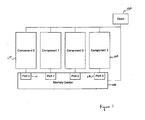
- FIG. 1 is a block diagram of an environment in which a multi-port memory device 100 having variable speed ports may operate.
- the multi-port memory device contains two or more serial ports 110, each port being couplable to a system component 120.
- the system component can be any type of component that uses shared memory, such as a baseband processor, media processor, or LCD controller, and may act as a port master to configure and control the port.
- the memory device 100 contains one or more banks of memory (not shown) that store data that may be accessed via the ports.
- the banks of memory may be made up of dynamic random access memory (DRAM) or other common types of memory
- DRAM dynamic random access memory
- a system clock 130 provides a common clocking signal that may be used by the memory device 100 and the components 120.
- Each component has a clock circuit (not shown) with appropriate bandwidth and jitter requirements.
- the system clock may be selectively divided at each port 110 so that each of the ports operates at a desired speed. Configuring the port speed on a port-by-port basis allows the port speed to be optimized to a corresponding component 120 that is attached to a port. While the communication between a port and attached component occurs at a configured speed, communication between the ports inside of the memory device occurs at a common speed.
- FIG. 2 is a block diagram of a clock distribution system 200 for the ports in the multi-port memory device.
- a phase-locked loop 210 generates two clock signals that are distributed to the ports 110: a system clock (sck) and a port clock (pck).
- the system clock is applied to the port logic 220 of each port, such as the parallel processing and communication of data from the port to the memory banks, enabling all port logic to operate at a common speed.
- the port clock is applied to a clock divider circuit 230 that is associated with each port. As will be described in additional detail herein, the clock divider circuit selectively modifies the port clock to a desired clock frequency on a port-by-port basis.
- Modifying the port clock frequency on a port-by-port basis enables various physical-layer components 240 of the port, such as the analog portion and the serial to parallel conversion of data at the port, to operate at a desired speed.
- the transmit and receive components of each port may be configured to operate with a coupled system component on a port-by-port basis.
- a clock domain boundary 250 is depicted in the figure to conceptually show that a portion of the physical layer operates at the local port clock speed and a portion of the physical layer operates at the system clock speed.
- the system clock speed is 150 MHz and the port clock speed is 750 MHz, although the system and port clock speeds may be varied to suit the system in which the disclosed architecture is utilized.
- a clock divider circuit 230 is depicted in the figure as being present at each port, it will be appreciated that only some of the ports in a multi-port memory device may include the clock divider circuit.
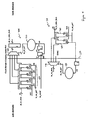
- FIG. 3 is a circuit diagram of the clock divider circuit 230 that divides a clock signal to a desired frequency.
- the divider circuit comprises two multiplexers 310, 320 that are connected in series, and a number of clock dividers 330 that each divide the clock frequency by a fixed amount.
- multiplexers 310 and 320 are 4-to-1 multiplexers.
- the port clock (pck) is directly connected to one input of the first multiplexer 310, and is connected to each of the other inputs of the first multiplexer through a set of clock dividers.
- the clock dividers associated with the three inputs have values of 3/4, 2/4, and 1/4.
- the first multiplexer may output a clock signal at the original port clock frequency, or the first multiplexer may output a clock signal that is reduced in frequency to either 75%, 50%, or 25% of the original port clock frequency.
- the output of the first multiplexer is determined by the setting of a mode register (MRS).
- MRS mode register
- the output of the first multiplexer is directly connected to one input of the second multiplexer 320, and is connected to the other inputs of the second multiplexer through a set of clock dividers.
- the clock dividers associated with the second multiplexer have values of 1/2, 1/4, and 1/8.
- the output of the second multiplexer is also determined by the setting of the mode register (MRS).
- the output of the second multiplexer is a local port clock (Ipck).
- the local port clock may range from the same frequency as the port clock (pck) to 1/32 of the frequency of the port clock in the depicted embodiment.
- a clock divider 340 is coupled to the output of the second multiplexer 320.
- Clock divider 340 divides the frequency of the local port clock by five. If the first and second multiplexers are set so that the local port clock (Ipck) is the same frequency as the port clock (pck), then in the depicted embodiment of FIGS. 2 and 3 , dividing the local port clock frequency by five will generate a local system clock (Isck) having the same frequency as the system clock (sck) (i.e., 750 MHz divided by five produces a 150 MHz clock signal).
- Figure 3 depicts a clock divider circuit with two multiplexers and certain clock divider values
- the configuration of the circuit may be modified depending on the particular application.
- the number of multiplexers, the number of inputs to each multiplexer, and the number and value of the clock dividers may all be varied depending on the application and the desired clock speeds.
- the value of the clock dividers 330 may be adjustable.
- Figure 4 is a circuit diagram of a transmit circuit 400 and a receive circuit 410 that extend across the clock domain boundary 250 in the multi-port memory device.
- the portions of the circuits to the left of the clock domain boundary 250 in the figure operate in the system clock (sck) domain.
- the portions of the circuits to the right of the clock domain boundary 250 operate in the local system clock (Isck) domain.
- the transmit circuit 400 is comprised of a set of four registers 430 that sequentially latch data that is received on the pl_tx_data lines. Bursts of data are received in four segments sized in accordance with the registers. The outputs from each of the registers are coupled to the inputs of a 4-to-1 multiplexer 450.
- a finite state machine 440 steps through the sequence 00, 01, 10, 11 and applies the sequence to the multiplexer 450 in order to select the output from each of the registers in sequence. The finite state machine sequence is only generated when the tx_valid signal is detected. Data is thereby transmitted on the pLtx_data_Isck lines. To avoid overflow of the registers, new data is received only when the previous four-segment burst of data has been processed.
- the receive circuit 410 is comprised of a pair of registers 460 that latch data that is received on the Ip_rx_data_Isck lines.
- the rx_wr_ptr signal alternates between 0 and 1, causing received data to be alternately latched into each register.
- Two registers are used to ensure that a read command does not overlap with a write command for data in a particular register.
- the outputs from each of the registers are coupled to the inputs of a multiplexer 470.
- a finite state machine 480 generates and applies a sequence to the multiplexer in order to select the appropriate output from the registers 460 and provide the received data on the tp_rx_data lines.
- all of the ports may be configured to operate at the highest speed setting available to each port.
- a port master may then selectively modify one or more of the ports to configure the ports for a desired application.
- a supervising port master may configure all of the ports of a device.
- aspects of the invention may be practiced with conventional systems.
- the construction and operation of the various blocks shown in the figures may be of conventional design, and need not be described in further detail herein to make and use the invention, because such blocks will be understood by those skilled in the relevant art.
- aspects of the system may be implemented using computer-executable instructions, such as program modules, executed by one or more computers or other devices.
- program modules include routines, programs, objects, components, data structures, and so on that perform particular tasks or implement particular abstract data types.
- the functionality of the program modules may be combined or distributed as desired in various embodiments.
Landscapes
- Engineering & Computer Science (AREA)
- Theoretical Computer Science (AREA)
- General Engineering & Computer Science (AREA)
- Physics & Mathematics (AREA)
- General Physics & Mathematics (AREA)
- Microelectronics & Electronic Packaging (AREA)
- Multimedia (AREA)
- Computer Hardware Design (AREA)
- Multi Processors (AREA)
- Static Random-Access Memory (AREA)
- Dram (AREA)
- Techniques For Improving Reliability Of Storages (AREA)
- Computer And Data Communications (AREA)
- Stored Programmes (AREA)
Claims (15)
- Mehrfachanschlussspeichervorrichtung, umfassend eine Vielzahl an Anschlüssen (110), die angeschlossenen Komponenten Zugang zu Speicherbanken bieten, wobei jeder Anschluss mit einer lokalen Anschlusstaktfrequenz arbeitet, und
ein Taktverteilungsnetzwerk (200) zur Verteilung eines Systemtaktsignals (sck) und eines Anschlusstaktsignals (pck) innerhalb der Speichervorrichtung, wobei das Systemtaktsignal eine Systemtaktfrequenz und das Anschlusstaktsignal eine Anschlusstaktfrequenz aufweist, und
die Vielzahl an Anschlüssen (110) mit dem Taktverteilungsnetzwerk verbunden ist und angeschlossenen Komponenten (120) Zugang zu den Speicherbanken mit der Systemtaktfrequenz bietet, worin das Systemtaktsignal und das Anschlusstaktsignal auf jeden der Vielzahl an Anschlüssen angelegt werden und worin jeder der Vielzahl an Anschlüssen eine damit verbundene Taktfrequenzteilerschaltung (230) mit einer ersten Vielzahl an Taktfrequenzteilern (330) und einer Vielzahl an Multiplexern (310, 320) umfasst, wobei die Taktfrequenzteilerschaltung das Anschlusstaktsignal empfängt und dazu verwendet, ein lokales Anschlusstaktsignal (Ipck) für den jeweiligen Anschluss mit einer lokalen Anschlusstaktfrequenz zu erzeugen, wobei die Taktfrequenzteilerschaltung ferner einen damit verbundenen zweiten Taktfrequenzteiler (340) umfasst, der das lokale Anschlusstaktsignal empfängt und die lokale Anschlusstaktfrequenz dazu verwendet, um ein lokales Systemtaktsignal (Isck) mit der Systemtaktfrequenz zu erzeugen, wobei das lokale Anschlusstaktsignal von dem zugeordneten Anschluss dazu verwendet wird, mit der lokalen Anschlusstaktfrequenz zu arbeiten,
worin jeder der Anschlüsse eine physikalische Schicht (240) umfasst, wobei die physikalische Schicht jedes Anschlusses einen ersten Teil, der das lokale Systemtaktsignal (Isck) empfängt und mit der Systemtaktfrequenz arbeitet, und einen zweiten Teil, der in der lokalen Anschlusstaktfrequenz arbeitet, umfasst. - Mehrfachanschlussspeichervorrichtung nach Anspruch 1, worin die Multiplexer (310, 320) der Taktfrequenzteilerschaltung jedes Anschlusses in Serie geschaltet sind.
- Speichervorrichtung mit mehreren Anschlüssen nach Anspruch 2, worin die Taktfrequenzteilerschaltung jedes Anschlusses das Anschlusstaktsignal modifiziert, indem jeder Multiplexer der Taktfrequenzteilerschaltung ein Eingangstaktsignal empfängt und entweder das Eingangstaktsignal ausgibt oder das Eingangstaktsignal durch einen gewählten Wert teilt, um ein Signal mit reduzierter Frequenz auszugeben.
- Mehrfachanschlussspeichervorrichtung nach Anspruch 3, worin die lokale Anschlusstaktfrequenz einen Bruchteil der Anschlusstaktfrequenz ausmacht.
- Mehrfachanschlussspeichervorrichtung nach Anspruch 1, worin die Kommunikation zwischen jedem der Vielzahl an Anschlüssen und jeder der Vielzahl an Speicherbanken mit der Systemtaktfrequenz erfolgt.
- Mehrfachanschlussspeichervorrichtung nach Anspruch 5, worin die Kommunikation zwischen jedem der Vielzahl an Anschlüssen und einer beliebigen mit dem jeweiligen Anschluss verbundenen Komponente mit der lokalen Anschlusstaktfrequenz erfolgt.
- Mehrfachanschlussspeichervorrichtung nach Anspruch 1, worin die Kommunikation zwischen der Vielzahl an Anschlüssen und den Speicherbanken parallel erfolgt.
- Mehrfachanschlussspeichervorrichtung nach Anspruch 1, worin die Kommunikation zwischen der Vielzahl an Anschlüssen und einer oder mehreren Komponenten, die mit der Vielzahl an Anschlüssen gekoppelt sind, seriell erfolgt.
- Mehrfachanschlussspeichervorrichtung nach Anspruch 1, worin die lokale Anschlusstaktfrequenz jedes der Vielzahl an Anschlüssen von Anschluss zu Anschluss variiert werden kann.
- Mehrfachanschlussspeichervorrichtung nach Anspruch 1, die ferner eine mit der Taktfrequenzteilerschaltung jedes Anschlusses verbundene Steuervorrichtung umfasst, worin die Steuervorrichtung die Modifizierung bestimmt, die von der Taktfrequenzteilerschaltung am Anschlusstaktsignal vorgenommen wird.
- Mehrfachanschlussspeichervorrichtung nach Anspruch 10, worin die Steuervorrichtung ein Steuerbefehlsregister ist.
- Mehrfachanschlussspeichervorrichtung nach Anspruch 1, worin die physikalische Schicht jedes Anschlusses ferner eine Senderschaltung (400) und eine Empfangsschaltung (410) umfasst.
- Mehrfachanschlussspeichervorrichtung nach Anspruch 12, worin ein erster Teil der Sendeschaltung und ein erster Teil der Empfangsschaltung jeder physikalischen Schicht im ersten Abschnitt der physikalischen Schicht vorliegen und ein zweiter Teil der Sendeschaltung und ein zweiter Teil der Empfangsschaltung der physikalischen Schicht im zweiten Abschnitt der physikalischen Schicht vorliegen.
- Mehrfachanschlussspeichervorrichtung nach Anspruch 13, worin der erste Teil der Sendeschaltung eine Vielzahl an Registern (430) zum Zwischenspeichern von Daten aus der Vielzahl an Speicherbanken umfasst und worin der zweite Teil der Sendeschaltung einen Multiplexer (450) zum Auswählen eines Ausgangs eines der Vielzahl an Registern umfasst.
- Mehrfachanschlussspeichervorrichtung nach Anspruch 13, worin der zweite Teil der Empfangsschaltung eine Vielzahl an Registern (460) zum Zwischenspeichern von auf dem Anschluss empfangenen Daten umfasst und worin der erste Teil der Empfangsschaltung einen Multiplexer (470) zum Auswählen eines Ausgangs eines der Vielzahl an Registern umfasst.
Applications Claiming Priority (2)
| Application Number | Priority Date | Filing Date | Title |
|---|---|---|---|
| US78840106P | 2006-03-30 | 2006-03-30 | |
| PCT/US2007/065723 WO2007115227A2 (en) | 2006-03-30 | 2007-03-30 | Multi-port memory device having variable port speeds |
Publications (2)
| Publication Number | Publication Date |
|---|---|
| EP2008281A2 EP2008281A2 (de) | 2008-12-31 |
| EP2008281B1 true EP2008281B1 (de) | 2012-01-25 |
Family
ID=38421761
Family Applications (2)
| Application Number | Title | Priority Date | Filing Date |
|---|---|---|---|
| EP07759902A Active EP2008281B1 (de) | 2006-03-30 | 2007-03-30 | Speichervorrichtung mit mehreren ports und verschiedenen port-geschwindigkeiten |
| EP07759901A Ceased EP2008164A2 (de) | 2006-03-30 | 2007-03-30 | Kommunikation zwischen ports bei einer speichervorrichtung mit mehreren ports |
Family Applications After (1)
| Application Number | Title | Priority Date | Filing Date |
|---|---|---|---|
| EP07759901A Ceased EP2008164A2 (de) | 2006-03-30 | 2007-03-30 | Kommunikation zwischen ports bei einer speichervorrichtung mit mehreren ports |
Country Status (7)
| Country | Link |
|---|---|
| US (2) | US7949863B2 (de) |
| EP (2) | EP2008281B1 (de) |
| JP (2) | JP5188493B2 (de) |
| KR (2) | KR101341286B1 (de) |
| CN (3) | CN101449262B (de) |
| TW (3) | TWI340982B (de) |
| WO (2) | WO2007115226A2 (de) |
Families Citing this family (52)
| Publication number | Priority date | Publication date | Assignee | Title |
|---|---|---|---|---|
| US9104599B2 (en) | 2007-12-06 | 2015-08-11 | Intelligent Intellectual Property Holdings 2 Llc | Apparatus, system, and method for destaging cached data |
| US8706968B2 (en) | 2007-12-06 | 2014-04-22 | Fusion-Io, Inc. | Apparatus, system, and method for redundant write caching |
| US8443134B2 (en) | 2006-12-06 | 2013-05-14 | Fusion-Io, Inc. | Apparatus, system, and method for graceful cache device degradation |
| US8489817B2 (en) | 2007-12-06 | 2013-07-16 | Fusion-Io, Inc. | Apparatus, system, and method for caching data |
| JP5523835B2 (ja) | 2006-12-06 | 2014-06-18 | フュージョン−アイオー,インコーポレイテッド | 高容量不揮発性ストレージ用のキャッシュとしてのソリッドステートストレージのための装置、システム、及び方法 |
| US7836226B2 (en) | 2007-12-06 | 2010-11-16 | Fusion-Io, Inc. | Apparatus, system, and method for coordinating storage requests in a multi-processor/multi-thread environment |
| US9519540B2 (en) | 2007-12-06 | 2016-12-13 | Sandisk Technologies Llc | Apparatus, system, and method for destaging cached data |
| DE102008011925B4 (de) * | 2008-02-29 | 2018-03-15 | Globalfoundries Inc. | Sicheres Initialisieren von Computersystemen |
| US8230180B2 (en) * | 2008-06-11 | 2012-07-24 | Samsung Electronics Co., Ltd. | Shared memory burst communications |
| KR20100085564A (ko) * | 2009-01-21 | 2010-07-29 | 삼성전자주식회사 | 데이터 처리 시스템과 데이터 처리 방법 |
| US8769213B2 (en) * | 2009-08-24 | 2014-07-01 | Micron Technology, Inc. | Multi-port memory and operation |
| JP2011058847A (ja) * | 2009-09-07 | 2011-03-24 | Renesas Electronics Corp | 半導体集積回路装置 |
| US9021158B2 (en) | 2009-09-09 | 2015-04-28 | SanDisk Technologies, Inc. | Program suspend/resume for memory |
| US8972627B2 (en) | 2009-09-09 | 2015-03-03 | Fusion-Io, Inc. | Apparatus, system, and method for managing operations for data storage media |
| US8289801B2 (en) * | 2009-09-09 | 2012-10-16 | Fusion-Io, Inc. | Apparatus, system, and method for power reduction management in a storage device |
| US9223514B2 (en) | 2009-09-09 | 2015-12-29 | SanDisk Technologies, Inc. | Erase suspend/resume for memory |
| US8458581B2 (en) * | 2009-10-15 | 2013-06-04 | Ansaldo Sts Usa, Inc. | System and method to serially transmit vital data from two processors |
| US8190944B2 (en) * | 2009-12-11 | 2012-05-29 | Ati Technologies Ulc | Device configured to switch a clock speed for multiple links running at different clock speeds and method for switching the clock speed |
| US8775856B1 (en) * | 2010-03-10 | 2014-07-08 | Smsc Holdings S.A.R.L. | System and method for generating clock signal for a plurality of communication ports by selectively dividing a reference clock signal with a plurality of ratios |
| JP2011227834A (ja) * | 2010-04-22 | 2011-11-10 | Sony Corp | 信号制御装置及び信号制御方法 |
| US8984216B2 (en) | 2010-09-09 | 2015-03-17 | Fusion-Io, Llc | Apparatus, system, and method for managing lifetime of a storage device |
| KR101796116B1 (ko) | 2010-10-20 | 2017-11-10 | 삼성전자 주식회사 | 반도체 장치, 이를 포함하는 메모리 모듈, 메모리 시스템 및 그 동작방법 |
| US10817502B2 (en) | 2010-12-13 | 2020-10-27 | Sandisk Technologies Llc | Persistent memory management |
| US9047178B2 (en) | 2010-12-13 | 2015-06-02 | SanDisk Technologies, Inc. | Auto-commit memory synchronization |
| US10817421B2 (en) | 2010-12-13 | 2020-10-27 | Sandisk Technologies Llc | Persistent data structures |
| US9208071B2 (en) | 2010-12-13 | 2015-12-08 | SanDisk Technologies, Inc. | Apparatus, system, and method for accessing memory |
| US9218278B2 (en) | 2010-12-13 | 2015-12-22 | SanDisk Technologies, Inc. | Auto-commit memory |
| EP2652623B1 (de) | 2010-12-13 | 2018-08-01 | SanDisk Technologies LLC | Vorrichtung, system, und verfahren für einen auto-commit-speicher |
| WO2012106362A2 (en) | 2011-01-31 | 2012-08-09 | Fusion-Io, Inc. | Apparatus, system, and method for managing eviction of data |
| WO2012112618A1 (en) * | 2011-02-14 | 2012-08-23 | The Regents Of The University Of California | Multi-band interconnect for inter-chip and intra-chip communications |
| WO2012116369A2 (en) | 2011-02-25 | 2012-08-30 | Fusion-Io, Inc. | Apparatus, system, and method for managing contents of a cache |
| CN102176138B (zh) * | 2011-03-01 | 2013-04-03 | 上海维宏电子科技股份有限公司 | 数控系统中硬件端口的对象化管理控制方法 |
| US8543774B2 (en) | 2011-04-05 | 2013-09-24 | Ansaldo Sts Usa, Inc. | Programmable logic apparatus employing shared memory, vital processor and non-vital communications processor, and system including the same |
| US9767032B2 (en) | 2012-01-12 | 2017-09-19 | Sandisk Technologies Llc | Systems and methods for cache endurance |
| US9251086B2 (en) | 2012-01-24 | 2016-02-02 | SanDisk Technologies, Inc. | Apparatus, system, and method for managing a cache |
| CN104123241B (zh) * | 2013-04-24 | 2017-08-29 | 华为技术有限公司 | 内存匿名页初始化方法、装置及系统 |
| US20140321471A1 (en) * | 2013-04-26 | 2014-10-30 | Mediatek Inc. | Switching fabric of network device that uses multiple store units and multiple fetch units operated at reduced clock speeds and related method thereof |
| US8963587B2 (en) * | 2013-05-14 | 2015-02-24 | Apple Inc. | Clock generation using fixed dividers and multiplex circuits |
| US9666244B2 (en) | 2014-03-01 | 2017-05-30 | Fusion-Io, Inc. | Dividing a storage procedure |
| US9665432B2 (en) * | 2014-08-07 | 2017-05-30 | Microsoft Technology Licensing, Llc | Safe data access following storage failure |
| US9847918B2 (en) | 2014-08-12 | 2017-12-19 | Microsoft Technology Licensing, Llc | Distributed workload reassignment following communication failure |
| US9933950B2 (en) | 2015-01-16 | 2018-04-03 | Sandisk Technologies Llc | Storage operation interrupt |
| US20160378151A1 (en) * | 2015-06-26 | 2016-12-29 | Intel Corporation | Rack scale architecture (rsa) and shared memory controller (smc) techniques of fast zeroing |
| US9690494B2 (en) * | 2015-07-21 | 2017-06-27 | Qualcomm Incorporated | Managing concurrent access to multiple storage bank domains by multiple interfaces |
| US9996138B2 (en) * | 2015-09-04 | 2018-06-12 | Mediatek Inc. | Electronic system and related clock managing method |
| CN105701026A (zh) * | 2016-01-04 | 2016-06-22 | 上海斐讯数据通信技术有限公司 | 一种数据采集器及其利用系统冗余资源采集数据的方法 |
| KR102757627B1 (ko) * | 2016-09-23 | 2025-01-23 | 삼성전자주식회사 | 케스-케이드 연결 구조로 레퍼런스 클록을 전달하는 스토리지 장치들을 포함하는 전자 장치 |
| KR102438319B1 (ko) * | 2018-02-07 | 2022-09-01 | 한국전자통신연구원 | 공통 메모리 인터페이스 장치 및 방법 |
| CN111142955B (zh) * | 2019-12-31 | 2021-07-16 | 联想(北京)有限公司 | 一种信息处理方法及装置 |
| CN114696819A (zh) * | 2020-12-31 | 2022-07-01 | 成都忆芯科技有限公司 | 可配置时钟的闪存通道及其存储设备 |
| US11567708B2 (en) * | 2021-01-05 | 2023-01-31 | Brother Kogyo Kabushiki Kaisha | Image forming apparatus having one or more ports to which portable memory is attachable |
| US12066855B2 (en) * | 2022-12-30 | 2024-08-20 | Arm Limited | Multi-port circuit architecture |
Family Cites Families (44)
| Publication number | Priority date | Publication date | Assignee | Title |
|---|---|---|---|---|
| US4344133A (en) * | 1978-07-31 | 1982-08-10 | Motorola, Inc. | Method for synchronizing hardware and software |
| US4449183A (en) * | 1979-07-09 | 1984-05-15 | Digital Equipment Corporation | Arbitration scheme for a multiported shared functional device for use in multiprocessing systems |
| US4729091A (en) * | 1984-11-13 | 1988-03-01 | International Business Machines Corporation | Directing storage requests prior to address comparator initialization with a reference address range |
| IT1184553B (it) * | 1985-05-07 | 1987-10-28 | Honeywell Inf Systems | Architettura di sistema a piu' processori |
| US5142683A (en) * | 1987-03-09 | 1992-08-25 | Unisys Corporation | Intercomputer communication control apparatus and method |
| JPH01501660A (ja) * | 1987-06-18 | 1989-06-08 | ユニシス・コーポレーシヨン | コンピユータ間通信制御装置及びその方法 |
| US5144314A (en) * | 1987-10-23 | 1992-09-01 | Allen-Bradley Company, Inc. | Programmable object identification transponder system |
| US4987529A (en) * | 1988-08-11 | 1991-01-22 | Ast Research, Inc. | Shared memory bus system for arbitrating access control among contending memory refresh circuits, peripheral controllers, and bus masters |
| US5197130A (en) * | 1989-12-29 | 1993-03-23 | Supercomputer Systems Limited Partnership | Cluster architecture for a highly parallel scalar/vector multiprocessor system |
| US5175853A (en) * | 1990-10-09 | 1992-12-29 | Intel Corporation | Transparent system interrupt |
| JPH04367963A (ja) * | 1991-06-15 | 1992-12-21 | Hitachi Ltd | 共有記憶通信方法 |
| US5423008A (en) | 1992-08-03 | 1995-06-06 | Silicon Graphics, Inc. | Apparatus and method for detecting the activities of a plurality of processors on a shared bus |
| JP3442128B2 (ja) * | 1994-02-21 | 2003-09-02 | 松下電工株式会社 | プロセッサ間通信方法および装置 |
| JP3447404B2 (ja) * | 1994-12-08 | 2003-09-16 | 日本電気株式会社 | マルチプロセッサシステム |
| US5925099A (en) * | 1995-06-15 | 1999-07-20 | Intel Corporation | Method and apparatus for transporting messages between processors in a multiple processor system |
| US6167487A (en) * | 1997-03-07 | 2000-12-26 | Mitsubishi Electronics America, Inc. | Multi-port RAM having functionally identical ports |
| US5901309A (en) * | 1997-10-07 | 1999-05-04 | Telefonaktiebolaget Lm Ericsson (Publ) | Method for improved interrupt handling within a microprocessor |
| US6118792A (en) * | 1997-11-21 | 2000-09-12 | Nortel Networks Corporation | Method and apparatus for a flexible access rate common-memory packet switch |
| US6313766B1 (en) * | 1998-07-01 | 2001-11-06 | Intel Corporation | Method and apparatus for accelerating software decode of variable length encoded information |
| US6263390B1 (en) * | 1998-08-18 | 2001-07-17 | Ati International Srl | Two-port memory to connect a microprocessor bus to multiple peripherals |
| KR100284741B1 (ko) * | 1998-12-18 | 2001-03-15 | 윤종용 | 로컬클럭 신호 발생회로 및 방법, 내부클럭신호 발생회로 및방법,이를 이용한 반도체 메모리 장치 |
| US6002633A (en) * | 1999-01-04 | 1999-12-14 | International Business Machines Corporation | Performance optimizing compiler for building a compiled SRAM |
| US6378051B1 (en) * | 1999-06-14 | 2002-04-23 | Maxtor Corporation | Interrupt signal prioritized shared buffer memory access system and method |
| US6396324B1 (en) * | 2000-05-08 | 2002-05-28 | International Business Machines Corporation | Clock system for an embedded semiconductor memory unit |
| US6845409B1 (en) * | 2000-07-25 | 2005-01-18 | Sun Microsystems, Inc. | Data exchange methods for a switch which selectively forms a communication channel between a processing unit and multiple devices |
| GB2370667B (en) * | 2000-09-05 | 2003-02-12 | Samsung Electronics Co Ltd | Semiconductor memory device having altered clock frequency for address and/or command signals, and memory module and system having the same |
| US6665795B1 (en) * | 2000-10-06 | 2003-12-16 | Intel Corporation | Resetting a programmable processor |
| US6938164B1 (en) * | 2000-11-22 | 2005-08-30 | Microsoft Corporation | Method and system for allowing code to be securely initialized in a computer |
| CZ20032079A3 (cs) * | 2001-01-31 | 2003-12-17 | International Business Machines Corporation | Způsob a zařízení pro přenos přerušení z periferního zařízení na hostitelský počítačový systém |
| US6877071B2 (en) | 2001-08-20 | 2005-04-05 | Technology Ip Holdings, Inc. | Multi-ported memory |
| US6795360B2 (en) * | 2001-08-23 | 2004-09-21 | Integrated Device Technology, Inc. | Fifo memory devices that support all four combinations of DDR or SDR write modes with DDR or SDR read modes |
| US7032106B2 (en) * | 2001-12-27 | 2006-04-18 | Computer Network Technology Corporation | Method and apparatus for booting a microprocessor |
| US7571287B2 (en) * | 2003-03-13 | 2009-08-04 | Marvell World Trade Ltd. | Multiport memory architecture, devices and systems including the same, and methods of using the same |
| CN1275143C (zh) * | 2003-06-11 | 2006-09-13 | 华为技术有限公司 | 数据处理系统及方法 |
| KR100606242B1 (ko) * | 2004-01-30 | 2006-07-31 | 삼성전자주식회사 | 불휘발성 메모리와 호스트간에 버퍼링 동작을 수행하는멀티 포트 휘발성 메모리 장치, 이를 이용한 멀티-칩패키지 반도체 장치 및 이를 이용한 데이터 처리장치 |
| JP4346506B2 (ja) * | 2004-06-07 | 2009-10-21 | 株式会社リコー | 先入れ先出しメモリ及びそれを用いた記憶媒体制御装置 |
| US20060073563A1 (en) * | 2004-09-02 | 2006-04-06 | Xencor, Inc. | Erythropoietin derivatives with altered immunogenicity |
| US20060072563A1 (en) | 2004-10-05 | 2006-04-06 | Regnier Greg J | Packet processing |
| JP2006301894A (ja) * | 2005-04-20 | 2006-11-02 | Nec Electronics Corp | マルチプロセッサシステム、及びマルチプロセッサシステムのメッセージ伝達方法 |
| JP2006309512A (ja) * | 2005-04-28 | 2006-11-09 | Nec Electronics Corp | マルチプロセッサシステム、及びマルチプロセッサシステムのメッセージ伝達方法 |
| JP4425243B2 (ja) * | 2005-10-17 | 2010-03-03 | Okiセミコンダクタ株式会社 | 半導体記憶装置 |
| US7369453B2 (en) * | 2006-02-28 | 2008-05-06 | Samsung Electronics Co., Ltd. | Multi-port memory device and method of controlling the same |
| US7433263B2 (en) * | 2006-02-28 | 2008-10-07 | Samsung Electronics Co., Ltd. | Multi-port semiconductor device and method thereof |
| KR100909805B1 (ko) * | 2006-09-21 | 2009-07-29 | 주식회사 하이닉스반도체 | 멀티포트 메모리 장치 |
-
2007
- 2007-03-30 JP JP2009503325A patent/JP5188493B2/ja active Active
- 2007-03-30 CN CN2007800183833A patent/CN101449262B/zh active Active
- 2007-03-30 EP EP07759902A patent/EP2008281B1/de active Active
- 2007-03-30 US US11/694,819 patent/US7949863B2/en active Active
- 2007-03-30 KR KR1020087026426A patent/KR101341286B1/ko active Active
- 2007-03-30 WO PCT/US2007/065722 patent/WO2007115226A2/en not_active Ceased
- 2007-03-30 CN CN2007800185044A patent/CN101449334B/zh active Active
- 2007-03-30 TW TW096111507A patent/TWI340982B/zh active
- 2007-03-30 TW TW096111504A patent/TWI353124B/zh active
- 2007-03-30 KR KR1020087026515A patent/KR101323400B1/ko active Active
- 2007-03-30 EP EP07759901A patent/EP2008164A2/de not_active Ceased
- 2007-03-30 WO PCT/US2007/065723 patent/WO2007115227A2/en not_active Ceased
- 2007-03-30 JP JP2009503324A patent/JP5197571B2/ja active Active
- 2007-03-30 TW TW096111501A patent/TWI386846B/zh active
- 2007-03-30 US US11/694,813 patent/US7639561B2/en active Active
- 2007-03-30 CN CN2007800160526A patent/CN101438242B/zh active Active
Also Published As
| Publication number | Publication date |
|---|---|
| JP5188493B2 (ja) | 2013-04-24 |
| TW200818734A (en) | 2008-04-16 |
| US20070245094A1 (en) | 2007-10-18 |
| JP2009532815A (ja) | 2009-09-10 |
| EP2008281A2 (de) | 2008-12-31 |
| CN101449334A (zh) | 2009-06-03 |
| CN101438242B (zh) | 2013-09-18 |
| US7949863B2 (en) | 2011-05-24 |
| TWI353124B (en) | 2011-11-21 |
| CN101449262A (zh) | 2009-06-03 |
| KR101341286B1 (ko) | 2013-12-12 |
| WO2007115226A3 (en) | 2008-10-30 |
| TWI386846B (zh) | 2013-02-21 |
| WO2007115226A2 (en) | 2007-10-11 |
| CN101449334B (zh) | 2012-04-25 |
| KR20090007378A (ko) | 2009-01-16 |
| CN101438242A (zh) | 2009-05-20 |
| US20070234021A1 (en) | 2007-10-04 |
| JP5197571B2 (ja) | 2013-05-15 |
| TWI340982B (en) | 2011-04-21 |
| WO2007115227A3 (en) | 2007-11-29 |
| TW200802403A (en) | 2008-01-01 |
| CN101449262B (zh) | 2012-07-04 |
| WO2007115227A2 (en) | 2007-10-11 |
| KR20080104388A (ko) | 2008-12-02 |
| JP2009532782A (ja) | 2009-09-10 |
| EP2008164A2 (de) | 2008-12-31 |
| KR101323400B1 (ko) | 2013-10-29 |
| TW200802082A (en) | 2008-01-01 |
| US7639561B2 (en) | 2009-12-29 |
Similar Documents
| Publication | Publication Date | Title |
|---|---|---|
| EP2008281B1 (de) | Speichervorrichtung mit mehreren ports und verschiedenen port-geschwindigkeiten | |
| US12235712B2 (en) | Dynamically changing data access bandwidth by selectively enabling and disabling data links | |
| US8683149B2 (en) | Reconfigurable memory controller | |
| US7934115B2 (en) | Deriving clocks in a memory system | |
| US20070033369A1 (en) | Reconfigurable integrated circuit device | |
| US9450620B1 (en) | Fast indirect antenna control | |
| US4509120A (en) | Variable cycle-time microcomputer | |
| US8754681B2 (en) | Multi-part clock management | |
| AU2004258478A1 (en) | Switch/network adapter port incorporating selectively accessible shared memory resources | |
| US20250068225A1 (en) | System on chip and application processor | |
| US20050278490A1 (en) | Memory access control apparatus and method of controlling memory access | |
| CN112486245B (zh) | 可重构阵列时钟门控控制方法、装置、设备及介质 | |
| US9202541B2 (en) | Semiconductor apparatus configured to reduce data processing performance | |
| US8743634B2 (en) | Generic low power strobe based system and method for interfacing memory controller and source synchronous memory | |
| KR20070047323A (ko) | 통신 인터페이스 요소를 포함하는 통신 모듈, 및 통신인터페이스 요소 | |
| JP2007018498A (ja) | プログラマブルロジックデバイスのシリアルインタフェースにおけるマルチプルデータレート | |
| CN111313869A (zh) | 一种千兆以太网收发器的时钟切换电路 | |
| JP6090017B2 (ja) | コンピュータシステム | |
| JP2006513489A (ja) | クラスタ化されたコンピュータシステムのための適応プロセッサノードのスケーラブルな相互接続のためのシステムおよび方法 |
Legal Events
| Date | Code | Title | Description |
|---|---|---|---|
| PUAI | Public reference made under article 153(3) epc to a published international application that has entered the european phase |
Free format text: ORIGINAL CODE: 0009012 |
|
| 17P | Request for examination filed |
Effective date: 20081021 |
|
| AK | Designated contracting states |
Kind code of ref document: A2 Designated state(s): AT BE BG CH CY CZ DE DK EE ES FI FR GB GR HU IE IS IT LI LT LU LV MC MT NL PL PT RO SE SI SK TR |
|
| AX | Request for extension of the european patent |
Extension state: AL BA HR MK RS |
|
| 17Q | First examination report despatched |
Effective date: 20090129 |
|
| DAX | Request for extension of the european patent (deleted) | ||
| RBV | Designated contracting states (corrected) |
Designated state(s): DE FR GB TR |
|
| GRAP | Despatch of communication of intention to grant a patent |
Free format text: ORIGINAL CODE: EPIDOSNIGR1 |
|
| GRAS | Grant fee paid |
Free format text: ORIGINAL CODE: EPIDOSNIGR3 |
|
| GRAA | (expected) grant |
Free format text: ORIGINAL CODE: 0009210 |
|
| AK | Designated contracting states |
Kind code of ref document: B1 Designated state(s): DE FR GB TR |
|
| REG | Reference to a national code |
Ref country code: GB Ref legal event code: FG4D |
|
| REG | Reference to a national code |
Ref country code: DE Ref legal event code: R096 Ref document number: 602007020265 Country of ref document: DE Effective date: 20120329 |
|
| PLBE | No opposition filed within time limit |
Free format text: ORIGINAL CODE: 0009261 |
|
| STAA | Information on the status of an ep patent application or granted ep patent |
Free format text: STATUS: NO OPPOSITION FILED WITHIN TIME LIMIT |
|
| 26N | No opposition filed |
Effective date: 20121026 |
|
| REG | Reference to a national code |
Ref country code: DE Ref legal event code: R097 Ref document number: 602007020265 Country of ref document: DE Effective date: 20121026 |
|
| PG25 | Lapsed in a contracting state [announced via postgrant information from national office to epo] |
Ref country code: TR Free format text: LAPSE BECAUSE OF FAILURE TO SUBMIT A TRANSLATION OF THE DESCRIPTION OR TO PAY THE FEE WITHIN THE PRESCRIBED TIME-LIMIT Effective date: 20120125 |
|
| REG | Reference to a national code |
Ref country code: FR Ref legal event code: PLFP Year of fee payment: 10 |
|
| REG | Reference to a national code |
Ref country code: FR Ref legal event code: PLFP Year of fee payment: 11 |
|
| REG | Reference to a national code |
Ref country code: FR Ref legal event code: PLFP Year of fee payment: 12 |
|
| PGFP | Annual fee paid to national office [announced via postgrant information from national office to epo] |
Ref country code: DE Payment date: 20250327 Year of fee payment: 19 |
|
| PGFP | Annual fee paid to national office [announced via postgrant information from national office to epo] |
Ref country code: FR Payment date: 20250325 Year of fee payment: 19 |
|
| PGFP | Annual fee paid to national office [announced via postgrant information from national office to epo] |
Ref country code: GB Payment date: 20250327 Year of fee payment: 19 |