EP2652623B1 - Vorrichtung, system, und verfahren für einen auto-commit-speicher - Google Patents
Vorrichtung, system, und verfahren für einen auto-commit-speicher Download PDFInfo
- Publication number
- EP2652623B1 EP2652623B1 EP11848174.6A EP11848174A EP2652623B1 EP 2652623 B1 EP2652623 B1 EP 2652623B1 EP 11848174 A EP11848174 A EP 11848174A EP 2652623 B1 EP2652623 B1 EP 2652623B1
- Authority
- EP
- European Patent Office
- Prior art keywords
- data
- commit
- auto
- memory
- host
- Prior art date
- Legal status (The legal status is an assumption and is not a legal conclusion. Google has not performed a legal analysis and makes no representation as to the accuracy of the status listed.)
- Active
Links
- 230000015654 memory Effects 0.000 title claims description 398
- 238000000034 method Methods 0.000 title claims description 80
- 238000003860 storage Methods 0.000 claims description 805
- 239000000872 buffer Substances 0.000 claims description 428
- 230000001960 triggered effect Effects 0.000 claims description 71
- 230000009471 action Effects 0.000 claims description 67
- 238000013507 mapping Methods 0.000 claims description 56
- 230000004044 response Effects 0.000 claims description 27
- 238000002955 isolation Methods 0.000 claims description 20
- 238000007726 management method Methods 0.000 description 101
- 238000010586 diagram Methods 0.000 description 32
- 230000002085 persistent effect Effects 0.000 description 31
- 239000008186 active pharmaceutical agent Substances 0.000 description 28
- 230000006870 function Effects 0.000 description 26
- 238000012937 correction Methods 0.000 description 24
- 230000006835 compression Effects 0.000 description 23
- 238000007906 compression Methods 0.000 description 23
- 238000012546 transfer Methods 0.000 description 23
- 230000007246 mechanism Effects 0.000 description 21
- 230000008569 process Effects 0.000 description 21
- 239000003795 chemical substances by application Substances 0.000 description 20
- 238000004891 communication Methods 0.000 description 19
- 238000004422 calculation algorithm Methods 0.000 description 12
- 238000013500 data storage Methods 0.000 description 11
- 230000006837 decompression Effects 0.000 description 10
- 239000011157 advanced composite material Substances 0.000 description 9
- 230000008901 benefit Effects 0.000 description 9
- 238000013459 approach Methods 0.000 description 8
- 230000008878 coupling Effects 0.000 description 8
- 238000010168 coupling process Methods 0.000 description 8
- 238000005859 coupling reaction Methods 0.000 description 8
- 238000005192 partition Methods 0.000 description 8
- 238000011112 process operation Methods 0.000 description 8
- 239000003990 capacitor Substances 0.000 description 7
- 238000001152 differential interference contrast microscopy Methods 0.000 description 7
- 230000009467 reduction Effects 0.000 description 7
- 238000005096 rolling process Methods 0.000 description 7
- 239000003550 marker Substances 0.000 description 6
- 230000036961 partial effect Effects 0.000 description 6
- 238000012545 processing Methods 0.000 description 6
- 238000011084 recovery Methods 0.000 description 6
- 230000003068 static effect Effects 0.000 description 6
- 230000001360 synchronised effect Effects 0.000 description 6
- 238000003491 array Methods 0.000 description 5
- 230000008859 change Effects 0.000 description 5
- 230000002829 reductive effect Effects 0.000 description 5
- 230000003139 buffering effect Effects 0.000 description 4
- 239000000835 fiber Substances 0.000 description 4
- 230000002093 peripheral effect Effects 0.000 description 4
- 239000007787 solid Substances 0.000 description 4
- 240000007643 Phytolacca americana Species 0.000 description 3
- 238000001514 detection method Methods 0.000 description 3
- 230000000694 effects Effects 0.000 description 3
- 238000005516 engineering process Methods 0.000 description 3
- 230000000977 initiatory effect Effects 0.000 description 3
- 238000002372 labelling Methods 0.000 description 3
- 238000012544 monitoring process Methods 0.000 description 3
- 238000012360 testing method Methods 0.000 description 3
- 230000004888 barrier function Effects 0.000 description 2
- 230000009286 beneficial effect Effects 0.000 description 2
- 230000005540 biological transmission Effects 0.000 description 2
- 238000004364 calculation method Methods 0.000 description 2
- 230000001419 dependent effect Effects 0.000 description 2
- 230000007613 environmental effect Effects 0.000 description 2
- 230000003370 grooming effect Effects 0.000 description 2
- 230000010354 integration Effects 0.000 description 2
- 239000000463 material Substances 0.000 description 2
- 238000000638 solvent extraction Methods 0.000 description 2
- 230000002459 sustained effect Effects 0.000 description 2
- 238000012795 verification Methods 0.000 description 2
- 206010000210 abortion Diseases 0.000 description 1
- 230000006978 adaptation Effects 0.000 description 1
- 230000004075 alteration Effects 0.000 description 1
- 238000003339 best practice Methods 0.000 description 1
- 230000002457 bidirectional effect Effects 0.000 description 1
- 230000000903 blocking effect Effects 0.000 description 1
- 239000011449 brick Substances 0.000 description 1
- 238000006243 chemical reaction Methods 0.000 description 1
- 230000000295 complement effect Effects 0.000 description 1
- 238000004590 computer program Methods 0.000 description 1
- 238000007596 consolidation process Methods 0.000 description 1
- 238000013523 data management Methods 0.000 description 1
- 238000012217 deletion Methods 0.000 description 1
- 230000037430 deletion Effects 0.000 description 1
- 238000013461 design Methods 0.000 description 1
- 238000009826 distribution Methods 0.000 description 1
- 230000009977 dual effect Effects 0.000 description 1
- 238000011010 flushing procedure Methods 0.000 description 1
- 230000036541 health Effects 0.000 description 1
- 230000008676 import Effects 0.000 description 1
- 238000003780 insertion Methods 0.000 description 1
- 230000037431 insertion Effects 0.000 description 1
- 230000000670 limiting effect Effects 0.000 description 1
- 238000012423 maintenance Methods 0.000 description 1
- 238000005259 measurement Methods 0.000 description 1
- 230000005055 memory storage Effects 0.000 description 1
- 238000013508 migration Methods 0.000 description 1
- 230000005012 migration Effects 0.000 description 1
- 238000012986 modification Methods 0.000 description 1
- 230000004048 modification Effects 0.000 description 1
- 230000003287 optical effect Effects 0.000 description 1
- 230000037361 pathway Effects 0.000 description 1
- 230000002688 persistence Effects 0.000 description 1
- 238000002360 preparation method Methods 0.000 description 1
- 230000002265 prevention Effects 0.000 description 1
- 230000000750 progressive effect Effects 0.000 description 1
- 230000000644 propagated effect Effects 0.000 description 1
- 238000010926 purge Methods 0.000 description 1
- 230000000717 retained effect Effects 0.000 description 1
- 230000002441 reversible effect Effects 0.000 description 1
- 239000004065 semiconductor Substances 0.000 description 1
- 238000012163 sequencing technique Methods 0.000 description 1
- 238000004513 sizing Methods 0.000 description 1
- 238000010561 standard procedure Methods 0.000 description 1
- 239000013589 supplement Substances 0.000 description 1
- 208000011580 syndromic disease Diseases 0.000 description 1
- 230000007704 transition Effects 0.000 description 1
- 238000013519 translation Methods 0.000 description 1
- 230000014616 translation Effects 0.000 description 1
Images


Classifications
-
- G—PHYSICS
- G06—COMPUTING; CALCULATING OR COUNTING
- G06F—ELECTRIC DIGITAL DATA PROCESSING
- G06F11/00—Error detection; Error correction; Monitoring
- G06F11/07—Responding to the occurrence of a fault, e.g. fault tolerance
- G06F11/16—Error detection or correction of the data by redundancy in hardware
- G06F11/1666—Error detection or correction of the data by redundancy in hardware where the redundant component is memory or memory area
-
- G—PHYSICS
- G06—COMPUTING; CALCULATING OR COUNTING
- G06F—ELECTRIC DIGITAL DATA PROCESSING
- G06F1/00—Details not covered by groups G06F3/00 - G06F13/00 and G06F21/00
- G06F1/26—Power supply means, e.g. regulation thereof
- G06F1/30—Means for acting in the event of power-supply failure or interruption, e.g. power-supply fluctuations
-
- G—PHYSICS
- G06—COMPUTING; CALCULATING OR COUNTING
- G06F—ELECTRIC DIGITAL DATA PROCESSING
- G06F11/00—Error detection; Error correction; Monitoring
- G06F11/07—Responding to the occurrence of a fault, e.g. fault tolerance
- G06F11/08—Error detection or correction by redundancy in data representation, e.g. by using checking codes
- G06F11/10—Adding special bits or symbols to the coded information, e.g. parity check, casting out 9's or 11's
- G06F11/1008—Adding special bits or symbols to the coded information, e.g. parity check, casting out 9's or 11's in individual solid state devices
-
- G—PHYSICS
- G06—COMPUTING; CALCULATING OR COUNTING
- G06F—ELECTRIC DIGITAL DATA PROCESSING
- G06F11/00—Error detection; Error correction; Monitoring
- G06F11/07—Responding to the occurrence of a fault, e.g. fault tolerance
- G06F11/14—Error detection or correction of the data by redundancy in operation
- G06F11/1402—Saving, restoring, recovering or retrying
- G06F11/1415—Saving, restoring, recovering or retrying at system level
- G06F11/1441—Resetting or repowering
-
- G—PHYSICS
- G06—COMPUTING; CALCULATING OR COUNTING
- G06F—ELECTRIC DIGITAL DATA PROCESSING
- G06F12/00—Accessing, addressing or allocating within memory systems or architectures
- G06F12/02—Addressing or allocation; Relocation
- G06F12/0223—User address space allocation, e.g. contiguous or non contiguous base addressing
- G06F12/023—Free address space management
- G06F12/0238—Memory management in non-volatile memory, e.g. resistive RAM or ferroelectric memory
- G06F12/0246—Memory management in non-volatile memory, e.g. resistive RAM or ferroelectric memory in block erasable memory, e.g. flash memory
-
- G—PHYSICS
- G06—COMPUTING; CALCULATING OR COUNTING
- G06F—ELECTRIC DIGITAL DATA PROCESSING
- G06F12/00—Accessing, addressing or allocating within memory systems or architectures
- G06F12/02—Addressing or allocation; Relocation
- G06F12/08—Addressing or allocation; Relocation in hierarchically structured memory systems, e.g. virtual memory systems
- G06F12/0802—Addressing of a memory level in which the access to the desired data or data block requires associative addressing means, e.g. caches
-
- G—PHYSICS
- G06—COMPUTING; CALCULATING OR COUNTING
- G06F—ELECTRIC DIGITAL DATA PROCESSING
- G06F3/00—Input arrangements for transferring data to be processed into a form capable of being handled by the computer; Output arrangements for transferring data from processing unit to output unit, e.g. interface arrangements
- G06F3/06—Digital input from, or digital output to, record carriers, e.g. RAID, emulated record carriers or networked record carriers
- G06F3/0601—Interfaces specially adapted for storage systems
- G06F3/0602—Interfaces specially adapted for storage systems specifically adapted to achieve a particular effect
- G06F3/0614—Improving the reliability of storage systems
- G06F3/0619—Improving the reliability of storage systems in relation to data integrity, e.g. data losses, bit errors
-
- G—PHYSICS
- G06—COMPUTING; CALCULATING OR COUNTING
- G06F—ELECTRIC DIGITAL DATA PROCESSING
- G06F3/00—Input arrangements for transferring data to be processed into a form capable of being handled by the computer; Output arrangements for transferring data from processing unit to output unit, e.g. interface arrangements
- G06F3/06—Digital input from, or digital output to, record carriers, e.g. RAID, emulated record carriers or networked record carriers
- G06F3/0601—Interfaces specially adapted for storage systems
- G06F3/0628—Interfaces specially adapted for storage systems making use of a particular technique
- G06F3/0655—Vertical data movement, i.e. input-output transfer; data movement between one or more hosts and one or more storage devices
- G06F3/0656—Data buffering arrangements
-
- G—PHYSICS
- G06—COMPUTING; CALCULATING OR COUNTING
- G06F—ELECTRIC DIGITAL DATA PROCESSING
- G06F3/00—Input arrangements for transferring data to be processed into a form capable of being handled by the computer; Output arrangements for transferring data from processing unit to output unit, e.g. interface arrangements
- G06F3/06—Digital input from, or digital output to, record carriers, e.g. RAID, emulated record carriers or networked record carriers
- G06F3/0601—Interfaces specially adapted for storage systems
- G06F3/0668—Interfaces specially adapted for storage systems adopting a particular infrastructure
- G06F3/0671—In-line storage system
- G06F3/0673—Single storage device
- G06F3/0679—Non-volatile semiconductor memory device, e.g. flash memory, one time programmable memory [OTP]
-
- G—PHYSICS
- G06—COMPUTING; CALCULATING OR COUNTING
- G06F—ELECTRIC DIGITAL DATA PROCESSING
- G06F11/00—Error detection; Error correction; Monitoring
- G06F11/07—Responding to the occurrence of a fault, e.g. fault tolerance
- G06F11/16—Error detection or correction of the data by redundancy in hardware
- G06F11/20—Error detection or correction of the data by redundancy in hardware using active fault-masking, e.g. by switching out faulty elements or by switching in spare elements
- G06F11/2015—Redundant power supplies
-
- G—PHYSICS
- G06—COMPUTING; CALCULATING OR COUNTING
- G06F—ELECTRIC DIGITAL DATA PROCESSING
- G06F11/00—Error detection; Error correction; Monitoring
- G06F11/30—Monitoring
- G06F11/3003—Monitoring arrangements specially adapted to the computing system or computing system component being monitored
- G06F11/3034—Monitoring arrangements specially adapted to the computing system or computing system component being monitored where the computing system component is a storage system, e.g. DASD based or network based
-
- G—PHYSICS
- G06—COMPUTING; CALCULATING OR COUNTING
- G06F—ELECTRIC DIGITAL DATA PROCESSING
- G06F11/00—Error detection; Error correction; Monitoring
- G06F11/30—Monitoring
- G06F11/3058—Monitoring arrangements for monitoring environmental properties or parameters of the computing system or of the computing system component, e.g. monitoring of power, currents, temperature, humidity, position, vibrations
-
- G—PHYSICS
- G06—COMPUTING; CALCULATING OR COUNTING
- G06F—ELECTRIC DIGITAL DATA PROCESSING
- G06F2201/00—Indexing scheme relating to error detection, to error correction, and to monitoring
- G06F2201/81—Threshold
-
- G—PHYSICS
- G06—COMPUTING; CALCULATING OR COUNTING
- G06F—ELECTRIC DIGITAL DATA PROCESSING
- G06F2212/00—Indexing scheme relating to accessing, addressing or allocation within memory systems or architectures
- G06F2212/72—Details relating to flash memory management
- G06F2212/7207—Details relating to flash memory management management of metadata or control data
Definitions
- This invention relates to auto-commit memory and more particularly to exposing auto commit memory to applications and/or operating systems.
- WO2004/077219 describes a system and method of mapping patterns of data, optimising disk read and write, verifying data integrity across clients and servers of different functionality having shared resources, and generally relates to a system and method for mapping patterns of persistent data in a format independent of application functionality so that the archived data allows accessibility, data exchange and sharing across multi-user applications independent of functionality without any external process of import or export in a common format understood by sharing applications.
- US2009/0172253 discloses apparatuses, systems, and computer program products that enable wear levelling of nonvolatile memory devices, such as flash memory devices.
- One or more embodiments include an apparatus that has a receiver and a wear levelling module.
- the receiver may receive low-level write requests to update direct-mapped values of nonvolatile memory.
- the wear levelling module may determine physical locations of the nonvolatile memory that correspond to logical locations of the write requests.
- modules may be implemented as a hardware circuit comprising custom VLSI circuits or gate arrays, off-the-shelf semiconductors such as logic chips, transistors, or other discrete components.
- a module may also be implemented in programmable hardware devices such as field programmable gate arrays, programmable array logic, programmable logic devices or the like.
- Modules may also be implemented in software for execution by various types of processors.
- An identified module of executable code may, for instance, comprise one or more physical or logical blocks of computer instructions which may, for instance, be organized as an object, procedure, or function. Nevertheless, the executables of an identified module need not be physically located together, but may comprise disparate instructions stored in different locations which, when joined logically together, comprise the module and achieve the stated purpose for the module.
- a module of executable code may be a single instruction, or many instructions, and may even be distributed over several different code segments, among different programs, and across several memory devices.
- operational data may be identified and illustrated herein within modules, and may be embodied in any suitable form and organized within any suitable type of data structure. The operational data may be collected as a single data set, or may be distributed over different locations including over different storage devices, and may exist, at least partially, merely as electronic signals on a system or network.
- the software portions are stored on one or more computer readable media.
- Reference to a computer readable medium may take any form capable of storing machine-readable instructions on a digital processing apparatus.
- a computer readable medium may be embodied by a compact disk, digital-video disk, a magnetic tape, a Bernoulli drive, a magnetic disk, a punch card, flash memory, integrated circuits, or other digital processing apparatus memory device.
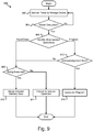
- the schematic flow chart diagrams included herein are generally set forth as logical flow chart diagrams. As such, the depicted order and labeled steps are indicative of one embodiment of the presented method. Other steps and methods may be conceived that are equivalent in function, logic, or effect to one or more steps, or portions thereof, of the illustrated method. Additionally, the format and symbols employed are provided to explain the logical steps of the method and are understood not to limit the scope of the method. Although various arrow types and line types may be employed in the flow chart diagrams, they are understood not to limit the scope of the corresponding method. Indeed, some arrows or other connectors may be used to indicate only the logical flow of the method. For instance, an arrow may indicate a waiting or monitoring period of unspecified duration between enumerated steps of the depicted method. Additionally, the order in which a particular method occurs may or may not strictly adhere to the order of the corresponding steps shown.
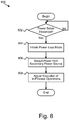
- Figure 1 depicts one embodiment of a system 100 for improved data management in the event of a power failure, power reduction, or other power loss.
- the system 100 includes a host computing device 114 and a storage device 102.
- the host 114 may be a computer such as a server, laptop, desktop, or other computing device known in the art.
- the host 114 typically includes components such as memory, processors, buses, and other components as known to those of skill in the art.
- the host 114 stores data in the storage device 102 and communicates data with the storage device 102 via a communications connection (not shown).
- the storage device 102 may be internal to the host 114 or external to the host 114.
- the communications connection may be a bus, a network, or other manner of connection allowing the transfer of data between the host 114 and the storage device 102.
- the storage device 102 is connected to the host 114 by a PCI connection such as PCI express ("PCI-e").
- PCI-e PCI express
- the storage device 102 may be a card that plugs into a PCI-e connection on the host 114.
- the storage device 102 also has a primary power connection 130 that connects the storage device 102 with a primary power source that provides the storage device 102 with the power that it needs to perform data storage operations such as reads, writes, erases, etc.
- the storage device 102 under normal operating conditions, receives the necessary power from the primary power source over the primary power connection 130.
- the primary power connection 130 connects the storage device 102 to the host 114, and the host 114 acts as the primary power source that supplies the storage device 102 with power.
- the primary power connection 130 and the communications connection discussed above are part of the same physical connection between the host 114 and the storage device 102.
- the storage device 102 may receive power over a PCI connection.
- the storage device 102 may connect to an external power supply via the primary power connection 130.
- the primary power connection 130 may connect the storage device 102 with a primary power source that is a power converter (often called a power brick).
- a power converter often called a power brick.
- the storage device 102 provides nonvolatile storage for the host 114.
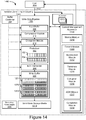
- Figure 1 shows the storage device 102 comprising a write data pipeline 106, a read data pipeline 108, nonvolatile memory 110, a storage controller 104, a power management apparatus 122, and a secondary power supply 124.
- the storage device 102 may contain additional components that are not shown in order to provide a simpler view of the storage device 102.
- the nonvolatile memory 110 stores data such that the data is retained even when the storage device 102 is not powered. Examples of nonvolatile memory 110 include solid state memory (such as Flash), hard disk, tape, or others.
- the storage device 102 also includes a storage controller 104 that coordinates the storage and retrieval of data in the nonvolatile memory 110.
- the storage controller 104 may use one or more indexes to locate and retrieve data, and perform other operations on data stored in the storage device 102.
- the storage controller 104 may include a groomer for performing data grooming operations such as garbage collection.
- the storage device 102 implements a write data pipeline 106 and a read data pipeline 108, an example of which is described in greater detail below with regard to Figure 3 .
- the write data pipeline 106 may perform certain operations on data as the data is transferred from the host 114 into the nonvolatile memory 110. These operations may include, for example, error correction code (ECC) generation, encryption, compression, and others.
- ECC error correction code
- the read data pipeline 108 may perform similar and potentially inverse operations on data that is being read out of nonvolatile memory 110 and sent to the host 114.
- the storage device 102 also includes a secondary power supply 124 that provides power in the event of a complete or partial power disruption resulting in the storage device 102 not receiving enough electrical power over the primary power connection 130.
- a power disruption is any event that unexpectedly causes the storage device 102 to stop receiving power over the primary power connection 130, or causes a significant reduction in the power received by the storage device 102 over the primary power connection 130.
- a significant reduction in power in one embodiment, includes the power falling below a predefined threshold.
- the predefined threshold in a further embodiment, is selected to allow for normal fluctuations in the level of power from the primary power connection 130. For example, the power to a building where the host 114 and the storage device 102 may go out.
- a user action (such as improperly shutting down the host 114 providing power to the storage device 102), a failure in the primary power connection 130, or a failure in the primary power supply may cause the storage device 102 to stop receiving power. Numerous, varied power disruptions may cause unexpected power loss for the storage device 102.
- the secondary power supply 124 may include one or more batteries, one or more capacitors, a bank of capacitors, a separate connection to a power supply, or the like. In one embodiment, the secondary power supply 124 provides power to the storage device 102 for at least a power hold-up time during a power disruption or other reduction in power from the primary power connection 130. The secondary power supply 124, in a further embodiment, provides a power hold-up time long enough to enable the storage device 102 to flush data that is not in nonvolatile memory 110 into the nonvolatile memory 110. As a result, the storage device 102 can preserve the data that is not permanently stored in the storage device 102 before the lack of power causes the storage device 102 to stop functioning.
- the secondary power supply 124 may comprise the smallest capacitors possible that are capable of providing a predefined power hold-up time to preserve space, reduce cost, and simplify the storage device 102.
- one or more banks of capacitors are used to implement the secondary power supply 124 as capacitors are generally more reliable, require less maintenance, and have a longer life than other options for providing secondary power.
- the secondary power supply 124 is part of an electrical circuit that automatically provides power to the storage device 102 upon a partial or complete loss of power from the primary power connection 130.
- the system 100 may be configured to automatically accept or receive electric power from the secondary power supply 124 during a partial or complete power loss.
- the secondary power supply 124 may be electrically coupled to the storage device 102 in parallel with the primary power connection 130, so that the primary power connection 130 charges the secondary power supply 124 during normal operation and the secondary power supply 124 automatically provides power to the storage device 102 in response to a power loss.
- the system 100 further includes a diode or other reverse current protection between the secondary power supply 124 and the primary power connection 130, to prevent current from the secondary power supply 124 from reaching the primary power connection 130.
- the power management apparatus 122 may enable or connect the secondary power supply 124 to the storage device 102 using a switch or the like in response to reduced power from the primary power connection 130.
- An example of data that is not yet in the nonvolatile memory 110 may include data that may be held in volatile memory as the data moves through the write data pipeline 106. If data in the write data pipeline 106 is lost during a power outage (i.e., not written to nonvolatile memory 110 or otherwise permanently stored), corruption and data loss may result.
- the storage device 102 sends an acknowledgement to the host 114 at some point after the storage device 102 receives data to be stored in the nonvolatile memory 110.
- the write data pipeline 106, or a sub-component thereof, may generate the acknowledgement. It is advantageous for the storage device 102 to send the acknowledgement as soon as possible after receiving the data.
- the write data pipeline 106 sends the acknowledgement before data is actually stored in the nonvolatile memory 110.
- the write data pipeline 106 may send the acknowledgement while the data is still in transit through the write data pipeline 106 to the nonvolatile memory 110.
- some data within the write data pipeline 106 may be corrupted as a result of the power disruption.
- a power disruption may include a power failure as well as unexpected changes in power levels supplied. The unexpected changes in power levels may place data that is in the storage device 102, but not yet in nonvolatile memory 110, at risk. Data corruption may begin to occur before the power management apparatus 122 is even aware (or notified) that there has been a disruption in power.
- PCI-e indicates that, in the event that a power disruption is signaled, data should be assumed corrupted and not stored in certain circumstances. Similar potential corruption may occur for storage devices 102 connected to hosts 114 using other connection types, such as PCI, serial advanced technology attachment (“serial ATA” or “SATA”), parallel ATA (“PATA”), small computer system interface (“SCSI”), IEEE 1394 (“FireWire”), Fiber Channel, universal serial bus (“USB”), PCIe-AS, or the like.
- serial ATA serial advanced technology attachment
- PATA parallel ATA
- SCSI small computer system interface
- IEEE 1394 FireWire
- Fiber Channel Fiber Channel
- USB universal serial bus
- PCIe-AS PCIe-AS
- a complication may arise when a power disruption occurs (meaning that data received from that point to the present time may be presumed corrupt), a period of time passes, the disruption is sensed and signaled, and the power management apparatus 122 receives the signal and becomes aware of the power disruption.
- the lag between the power disruption occurring and the power management apparatus 122 discovering the power disruption can allow corrupt data to enter the write data pipeline 106.
- this corrupt data should be identified and not stored to the nonvolatile memory 110.
- this corrupt data can be stored in the nonvolatile memory 110 and marked as corrupt as described below.
- identifying corrupt data and not storing the data to the nonvolatile memory 110 will be primarily used to describe the functions and features herein.
- the host 114 should be aware that this data was not stored, or alternatively data for which integrity is a question is not acknowledged until data integrity can be verified. As a result, corrupt data should not be acknowledged.
- the storage device 102 also includes a power management apparatus 122.
- the power management apparatus 122 is implemented as part of the storage controller 104.
- the power management apparatus 122 may be, for instance, a software driver or be implemented in firmware for the storage device 102.
- the power management apparatus 122 may be implemented partially in a software driver and partially in the storage controller 104, or the like.
- at least a portion of the power management apparatus 122 is implemented on the storage device 102, as part of the storage controller 104, or the like, so that the power management apparatus 122 continues to function during a partial or complete power loss using power from the secondary power supply 124, even if the host 114 is no longer functioning.
- the power management apparatus 122 initiates a power loss mode in the storage device 102 in response to a reduction in power from the primary power connection 130.
- the power management apparatus 122 flushes data that is in the storage device 102 that is not yet stored in nonvolatile memory 110 into the nonvolatile memory 110.
- the power management apparatus 122 flushes the data that has been acknowledged and is in the storage device 102 that is not yet stored in nonvolatile memory 110 into the nonvolatile memory 110.
- the power management apparatus 122 may adjust execution of data operations on the storage device 102 to ensure that essential operations complete before the secondary power supply 124 loses sufficient power to complete the essential operations, i.e. during the power hold-up time that the secondary power supply 124 provides.
- the essential operations comprise those operations for data that has been acknowledged as having been stored, such as acknowledged write operations. In other embodiments, the essential operations comprise those operations for data that has been acknowledged as having been stored and erased. In other embodiments, the essential operations comprise those operations for data that have been acknowledged as having been stored, read, and erased.
- the power management apparatus 122 may also terminate non-essential operations to ensure that those non-essential operations do not consume power unnecessarily and/or do not block essential operations from executing; for example, the power management apparatus 122 may terminate erase operations, read operations, unacknowledged write operations, and the like.
- terminating non-essential operations preserves power from the secondary power supply 124, allowing the secondary power supply 124 to provide the power hold-up time.
- the power management apparatus 122 quiesces or otherwise shuts down operation of one or more subcomponents of the storage device 102 during the power loss mode to conserve power from the secondary power supply 124.
- the power management apparatus 122 may quiesce operation of the read data pipeline 108, a read direct memory access (“DMA") engine, and/or other subcomponents of the storage device 102 that are associated with non-essential operations.
- DMA read direct memory access
- the power management apparatus 122 may also be responsible for determining what data was corrupted by the power disruption, preventing the corrupt data from being stored in nonvolatile memory 110, and ensuring that the host 114 is aware that the corrupted data was never actually stored on the storage device 102. This prevents corruption of data in the storage device 102 resulting from the power disruption.
- the system 100 includes a plurality of storage devices 102.
- the power management apparatus 122 manages power loss modes for each storage device 102 in the plurality of storage devices 102, providing a system-wide power loss mode for the plurality of storage devices 102.
- each storage device 102 in the plurality of storage devices 102 includes a separate power management apparatus 122 that manages a separate power loss mode for each individual storage device 102.
- the power management apparatus 122 may quiesce or otherwise shut down one or more storage devices 102 of the plurality of storage devices 102 to conserve power from the secondary power supply 124 for executing essential operations on one or more other storage devices 102.
- the system 100 includes one or more adapters for providing electrical connections between the host 114 and the plurality of storage devices 102.
- An adapter in various embodiments, may include a slot or port that receives a single storage device 102, an expansion card or daughter card that receives two or more storage devices 102, or the like.
- the plurality of storage devices 102 may each be coupled to separate ports or slots of the host 114.
- one or more adapters such as daughter cards or the like, may be electrically coupled to the host 114 (i.e. connected to one or more slots or ports of the host 114) and the one or more adapters may each provide connections for two or more storage devices 102.
- the system 100 includes a circuit board, such as a motherboard or the like, that receives two or more adapters, such as daughter cards or the like, and each adapter receives two or more storage devices 102.
- the adapters are coupled to the circuit board using PCI-e slots of the circuit board and the storage devices 102 are coupled to the adapters using PCI-e slots of the adapters.
- the storage devices 102 each comprise a dual in-line memory module ("DIMM") of non-volatile solid-state storage, such as Flash memory, or the like.
- the circuit board, the adapters, and the storage devices 102 may be external to the host 114, and may include a separate primary power connection 130.
- the circuit board, the adapters, and the storage devices 102 may be housed in an external enclosure with a power supply unit ("PSU") and may be in communication with the host 114 using an external bus such as eSATA, eSATAp, SCSI, FireWire, Fiber Channel, USB, PCIe-AS, or the like.
- PSU power supply unit
- the circuit board may be a motherboard of the host 114, and the adapters and the storage devices 102 may be internal storage of the host 114.
- each adapter may receive two storage devices 102, four storage devices 102, or any number of storage devices.
- the system 100 may include one adapter, two adapters, three adapters, four adapters, or any supported number of adapters.
- the system 100 includes two adapters and each adapter receives four storage devices 102, for a total of eight storage devices 102.
- the secondary power supply 124 provides electric power to each of a plurality of storage devices 102.
- the secondary power supply 124 may be disposed in a circuit on a main circuit board or motherboard and may provide power to several adapters.
- the system 100 includes a plurality of secondary power supplies that each provide electric power to a subset of a plurality of storage devices 102.
- each adapter may include a secondary power supply 124 for storage devices 102 of the adapter.
- each storage device 102 may include a secondary power supply 124 for the storage device 102.
- secondary power supplies 124 for providing power to a plurality of storage devices 102.
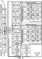
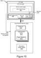
- FIG. 2 is a schematic block diagram illustrating one embodiment 200 of a solid-state storage device controller 202 that includes a write data pipeline 106 and a read data pipeline 108 in a solid-state storage device 102 in accordance with the present invention.
- the solid-state storage device controller 202 may include a number of solid-state storage controllers 0-N 104a-n, each controlling solid-state storage media 110.
- solid-state controller 0 104a two solid-state controllers are shown: solid-state controller 0 104a and solid-state storage controller N 104n, and each controlling respective solid-state storage media 110a-n.
- solid-state storage controller 0 104a controls a data channel so that the attached solid-state storage media 110a stores data.
- Solid-state storage controller N 104n controls an index metadata channel associated with the stored data and the associated solid-state storage media 110n stores index metadata.
- the solid-state storage device controller 202 includes a single solid-state controller 104a with a single solid-state storage media 110a.
- At least one solid-state controller 104 is a field-programmable gate array ("FPGA") and controller functions are programmed into the FPGA.
- the FPGA is a Xilinx® FPGA.
- the solid-state storage controller 104 comprises components specifically designed as a solid-state storage controller 104, such as an application-specific integrated circuit ("ASIC") or custom logic solution.
- ASIC application-specific integrated circuit
- Each solid-state storage controller 104 typically includes a write data pipeline 106 and a read data pipeline 108, which are describe further in relation to Figure 3 .
- at least one solid-state storage controller 104 is made up of a combination FPGA, ASIC, and custom logic components.
- the solid-state storage media 110 is an array of non-volatile solid-state storage elements 216, 218, 220, arranged in banks 214, and accessed in parallel through a bi-directional storage input/output ("I/O") bus 210.
- the storage I/O bus 210 in one embodiment, is capable of unidirectional communication at any one time. For example, when data is being written to the solid-state storage media 110, data cannot be read from the solid-state storage media 110. In another embodiment, data can flow both directions simultaneously.
- bi-directional refers to a data pathway that can have data flowing in only one direction at a time, but when data flowing one direction on the bi-directional data bus is stopped, data can flow in the opposite direction on the bi-directional data bus.
- a solid-state storage element (e.g., SSS 0.0 216a) is typically configured as a chip (a package of one or more dies) or a die on a circuit board.
- a solid-state storage element (e.g., 216a) operates independently or semi-independently of other solid-state storage elements (e.g., 218a) even if these several elements are packaged together in a chip package, a stack of chip packages, or some other package element.
- a row of solid-state storage elements 216a, 216b, 216m is designated as a bank 214.
- n there may be "n" banks 214a-n and "m” solid-state storage elements 216a-m, 218a-m, 220a-m per bank in an array of n x m solid-state storage elements 216, 218, 220 in a solid-state storage media 110.
- a solid-state storage media 110a includes twenty solid-state storage elements 216a-216m per bank 214 with eight banks 214.
- the solid-state storage media 110a includes twenty-four solid-state storage elements 216a-216m per bank 214 with eight banks 214.
- each solid-state storage element 216, 218, 220 is comprised of single-level cell (“SLC") devices.
- SLC single-level cell
- MLC multi-level cell
- solid-state storage elements that share a common line 211 on the storage I/O bus 210a are packaged together.
- a solid-state storage element 216, 218, 220 may have one or more dies per package with one or more packages stacked vertically and each die may be accessed independently.
- a solid-state storage element e.g., SSS 0.0 216a
- SSS 0.0 216a may have one or more virtual dies per die and one or more dies per package and one or more packages stacked vertically and each virtual die may be accessed independently.
- a solid-state storage element SSS 0.0 216a may have one or more virtual dies per die and one or more dies per package with some or all of the one or more dies stacked vertically and each virtual die may be accessed independently.
- two dies are stacked vertically with four stacks per group to form eight storage elements (e.g., SSS 0.0-SSS 8.0) 216a, 218a ... 220a, each in a separate bank 214a, 214b ... 214n.
- 24 storage elements e.g., SSS 0.0-SSS 0.24) 216a, 216b, ... 216m form a logical bank 214a so that each of the eight logical banks has 24 storage elements (e.g., SSS0.0-SSS 8.24) 216, 218, 220.
- Data is sent to the solid-state storage media 110 over the storage I/O bus 210 to all storage elements of a particular group of storage elements (SSS 0.0-SSS 8.0) 216a, 218a, 220a.
- the storage control bus 212a is used to select a particular bank (e.g., Bank 0 214a) so that the data received over the storage I/O bus 210 connected to all banks 214 is written just to the selected bank 214a.
- the storage I/O bus 210 is comprised of one or more independent I/O buses ("IIOBa-m" comprising 210a.a-m ... 210n.a-m) wherein the solid-state storage elements within each column share one of the independent I/O buses that are connected to each solid-state storage element 216, 218, 220 in parallel.
- IIOBa-m independent I/O buses
- one independent I/O bus 210a.a of the storage I/O bus 210a may be physically connected to a first solid-state storage element 216a, 218a, 220a of each bank 214a-n.
- a second independent I/O bus 210a.b of the storage I/O bus 210b may be physically connected to a second solid-state storage element 216b, 218b, 220b of each bank 214a-n.
- Each solid-state storage element 216a, 216b, 216m in a bank 214a (a row of solid-state storage elements as illustrated in Fig. 2 ) may be accessed simultaneously and/or in parallel.
- solid-state storage elements 216, 218, 220 comprise stacked packages of dies
- all packages in a particular stack are physically connected to the same independent I/O bus.
- "simultaneously” also includes near simultaneous access where devices are accessed at slightly different intervals to avoid switching noise. Simultaneously is used in this context to be distinguished from a sequential or serial access wherein commands and/or data are sent individually one after the other.
- banks 214a-n are independently selected using the storage control bus 212.
- a bank 214 is selected using a chip enable or chip select. Where both chip select and chip enable are available, the storage control bus 212 may select one package within a stack of packages. In other embodiments, other commands are used by the storage control bus 212 to individually select one package within a stack of packages.
- Solid-state storage elements 216, 218, 220 may also be selected through a combination of control signals and address information transmitted on storage I/O bus 210 and the storage control bus 212.
- each solid-state storage element 216, 218, 220 is partitioned into erase blocks and each erase block is partitioned into pages.
- An erase block on a solid-state storage element 216, 218 220 may be called a physical erase block or "PEB."
- a typical page is 2048 bytes ("2kB").
- a solid-state storage element e.g., SSS 0.0
- SSS 0.0 includes two registers and can program two pages so that a two-register solid-state storage element 216, 218, 220 has a capacity of 4kB.
- a bank 214 of 20 solid-state storage elements 216a, 216b, 216m would then have an 80kB capacity of pages accessed with the same address going out the independent I/O buses of the storage I/O bus 210.
- This group of pages in a bank 214 of solid-state storage elements 216a, 216b, ... 216m of 80kB may be called a logical page or virtual page.
- an erase block of each storage element 216a, 216b, ... 216m of a bank 214a may be grouped to form a logical erase block (which may also be called a virtual erase block).
- an erase block of pages within a solid-state storage element is erased when an erase command is received within the solid-state storage element.
- a physical address is sent on the storage I/O bus 210 and is followed by the packet.
- the physical address contains enough information for the solid-state storage element 216to direct the packet to the designated location within the page. Since all storage elements in a column of storage elements (e.g., SSS 0.0-SSS N.0 216a, 218a, ...
- the bank 214a that includes the solid-state storage element SSS 0.0 216a with the correct page where the data packet is to be written is selected by the storage control bus 212a and other banks 214b ... 214n of the solid-state storage 110a are deselected.
- a read command on the storage I/O bus 210 requires a signal on the storage control bus 212 to select a single bank 214a and the appropriate page within that bank 214a.
- a read command reads an entire page, and because there are multiple solid-state storage elements 216a, 216b, ... 216m in parallel in a bank 214a, an entire logical page is read with a read command.
- the read command may be broken into subcommands, as will be explained below with respect to bank interleave.
- an entire logical page may be written to the solid-state storage elements 216a, 216b, ... 216m of a bank 214a in a write operation.
- An erase block erase command may be sent out to erase an erase block over the storage I/O bus 210 with a particular erase block address to erase a particular erase block.
- storage controller 104a may send an erase block erase command over the parallel paths (independent I/O buses 210a-n.a-m) of the storage I/O bus 210 to erase a logical erase block, each with a particular erase block address to erase a particular erase block.
- a particular bank e.g., Bank 0 214a
- no particular bank e.g., Bank 0 214a
- the storage control bus 212 or all of the banks are selected to enable erasure of similarly addressed erase blocks in all of the banks (Banks 1-N 214b-n) in parallel.
- Other commands may also be sent to a particular location using a combination of the storage I/O bus 210 and the storage control bus 212.
- One of skill in the art will recognize other ways to select a particular storage location using the bi-directional storage I/O bus 210 and the storage control bus 212.
- packets are written sequentially to the solid-state storage media 110.
- storage controller 104a streams packets to storage write buffers of a bank 214a of storage elements 216 and, when the buffers are full, the packets are programmed to a designated logical page.
- Storage controller 104a then refills the storage write buffers with packets and, when full, the packets are written to the next logical page.
- the next logical page may be in the same bank 214a or another bank (e.g., 214b).
- This process continues, logical page after logical page, typically until a logical erase block is filled.
- the streaming may continue across logical erase block boundaries with the process continuing, logical erase block after logical erase block.
- a read, modify, write operation data packets associated with requested data are located and read in a read operation.
- Data segments of the modified requested data that have been modified are not written to the location from which they are read. Instead, the modified data segments are again converted to data packets and then written sequentially to the next available location in the logical page currently being written.
- the index entries for the respective data packets are modified to point to the packets that contain the modified data segments.
- the entry or entries in the index for data packets associated with the same requested data that have not been modified will include pointers to original location of the unmodified data packets.
- the original requested data is maintained, for example to maintain a previous version of the requested data, the original requested data will have pointers in the index to all data packets as originally written.
- the new requested data will have pointers in the index to some of the original data packets and pointers to the modified data packets in the logical page that is currently being written.
- the index includes an entry for the original requested data mapped to a number of packets stored in the solid-state storage media 110.
- a new copy of the requested data is created and a new entry is created in the index mapping the new copy of the requested data to the original packets.
- the new copy of the requested data is also written to the solid-state storage media 110 with its location mapped to the new entry in the index.
- the new copy of the requested data packets may be used to identify the packets within the original requested data that are referenced in case changes have been made in the original requested data that have not been propagated to the copy of the requested data and the index is lost or corrupted.
- sequentially writing packets facilitates a more even use of the solid-state storage media 110 and allows the solid-storage device controller 202 to monitor storage hot spots and level usage of the various logical pages in the solid-state storage media 110. Sequentially writing packets also facilitates a powerful, efficient garbage collection system, which is described in detail below. One of skill in the art will recognize other benefits of sequential storage of data packets.
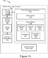
- the solid-state storage device controller 202 also includes a data bus 204, a local bus 206, a buffer controller 208, buffers 0-N 222a-n, a master controller 224, a direct memory access (“DMA") controller 226, a memory controller 228, a dynamic memory array 230, a static random memory array 232, a management controller 234, a management bus 236, a bridge 238 to a system bus 240, and miscellaneous logic 242, which are described below.
- DMA direct memory access
- the system bus 240 is coupled to one or more network interface cards (“NICs”) 244, some of which may include remote DMA (“RDMA”) controllers 246, one or more central processing unit (“CPU”) 248, one or more external memory controllers 250 and associated external memory arrays 252, one or more storage controllers 254, peer controllers 256, and application specific processors 258, which are described below.
- NICs network interface cards
- RDMA remote DMA
- CPU central processing unit
- external memory controllers 250 and associated external memory arrays 252 one or more storage controllers 254, peer controllers 256, and application specific processors 258, which are described below.
- the components 244-258 connected to the system bus 240 may be located in the host computing system 114 or may be other devices.
- the solid-state storage controller(s) 104 communicate data to the solid-state storage media 110 over a storage I/O bus 210.
- the storage I/O bus 210 is an array of busses, one for each column of storage elements 216, 218, 220 spanning the banks 214.
- the term "storage I/O bus” may refer to one storage I/O bus 210 or an array of independent data busses wherein individual data busses of the array independently communicate different data relative to one another.
- each storage I/O bus 210 accessing a column of storage elements may include a logical-to-physical mapping for storage divisions (e.g., erase blocks) accessed in a column of storage elements 216a, 218a, 220a.
- This mapping (or bad block remapping) allows a logical address mapped to a physical address of a storage division to be remapped to a different storage division if the first storage division fails, partially fails, is inaccessible, or has some other problem.
- Data may also be communicated to the solid-state storage controller(s) 104 from a requesting device 155 through the system bus 240, bridge 238, local bus 206, buffer(s) 222, and finally over a data bus 204.
- the data bus 204 typically is connected to one or more buffers 222a-n controlled with a buffer controller 208.
- the buffer controller 208 typically controls transfer of data from the local bus 206 to the buffers 222 and through the data bus 204 to the pipeline input buffer 306 and output buffer 330.
- the buffer controller 208 typically controls how data arriving from a requesting device can be temporarily stored in a buffer 222 and then transferred onto a data bus 204, or vice versa, to account for different clock domains, to prevent data collisions, etc.
- the buffer controller 208 typically works in conjunction with the master controller 224 to coordinate data flow. As data arrives, the data will arrive on the system bus 240, be transferred to the local bus 206 through a bridge 238.
- the data is transferred from the local bus 206 to one or more data buffers 222 as directed by the master controller 224 and the buffer controller 208.
- the data then flows out of the buffer(s) 222 to the data bus 204, through a solid-state controller 104, and on to the solid-state storage media 110 such as NAND flash or other storage media.
- data and associated out-of-band metadata (“metadata”) arriving with the data is communicated using one or more data channels comprising one or more solid-state storage controllers 104a-104n-1 and associated solid-state storage media 110a-110n-1 while at least one channel (solid-state storage controller 104n, solid-state storage media 110n) is dedicated to in-band metadata, such as index information and other metadata generated internally to the solid-state storage device 102.
- solid-state storage controller 104n, solid-state storage media 110n is dedicated to in-band metadata, such as index information and other metadata generated internally to the solid-state storage device 102.
- the local bus 206 is typically a bidirectional bus or set of busses that allows for communication of data and commands between devices internal to the solid-state storage device controller 202 and between devices internal to the solid-state storage device 102 and devices 244-258 connected to the system bus 240.
- the bridge 238 facilitates communication between the local bus 206 and system bus 240.
- One of skill in the art will recognize other embodiments such as ring structures or switched star configurations and functions of buses 240, 206, 204, 210 and bridges 238.
- the system bus 240 is typically a bus of a host computing system 114 or other device in which the solid-state storage device 102 is installed or connected.
- the system bus 240 may be a PCI-e bus, a Serial Advanced Technology Attachment ("serial ATA") bus, parallel ATA, or the like.
- the system bus 240 is an external bus such as small computer system interface ("SCSI"), FireWire, Fiber Channel, USB, PCIe-AS, or the like.
- SCSI small computer system interface
- FireWire FireWire
- Fiber Channel Universal Serial Bus
- USB Peripheral Component Interconnect Express
- the solid-state storage device controller 202 includes a master controller 224 that controls higher-level functions within the solid-state storage device 102.
- the master controller 224 controls data flow by interpreting object requests and other requests, directs creation of indexes to map object identifiers associated with data to physical locations of associated data, coordinating DMA requests, etc. Many of the functions described herein are controlled wholly or in part by the master controller 224.
- the master controller 224 uses embedded controller(s). In another embodiment, the master controller 224 uses local memory such as a dynamic memory array 230 (dynamic random access memory "DRAM"), a static memory array 232 (static random access memory “SRAM”), etc. In one embodiment, the local memory is controlled using the master controller 224. In another embodiment, the master controller 224 accesses the local memory via a memory controller 228. In another embodiment, the master controller 224 runs a Linux server and may support various common server interfaces, such as the World Wide Web, hyper-text markup language (“HTML”), etc. In another embodiment, the master controller 224 uses a nano-processor. The master controller 224 may be constructed using programmable or standard logic, or any combination of controller types listed above. One skilled in the art will recognize many embodiments for the master controller 224.
- DRAM dynamic random access memory
- SRAM static memory array
- the local memory is controlled using the master controller 224.
- the master controller 224 accesses the local memory via a memory controller 228.
- the master controller 224 divides the work load among internal controllers, such as the solid-state storage controllers 104a-n. For example, the master controller 224 may divide an object to be written to the data storage devices (e.g., solid-state storage media 110a-n) so that a portion of the object is stored on each of the attached data storage devices. This feature is a performance enhancement allowing quicker storage and access to an object.
- the master controller 224 is implemented using an FPGA.
- the firmware within the master controller 224 may be updated through the management bus 236, the system bus 240 over a network connected to a NIC 244 or other device connected to the system bus 240.
- the master controller 224 which manages objects, emulates block storage such that a host computing system 114 or other device connected to the storage device/solid-state storage device 102 views the storage device/solid-state storage device 102 as a block storage device and sends data to specific physical addresses in the storage device/solid-state storage device 102.
- the master controller 224 then divides up the blocks and stores the data blocks as it would objects.
- the master controller 224 then maps the blocks and physical address sent with the block to the actual locations determined by the master controller 224. The mapping is stored in the object index.
- a block device application program interface (“API") is provided in a driver in a computer such as the host computing system 114, or other device wishing to use the storage device/solid-state storage device 102 as a block storage device.
- API application program interface
- the master controller 224 coordinates with NIC controllers 244 and embedded RDMA controllers 246 to deliver just-in-time RDMA transfers of data and command sets.
- NIC controller 244 may be hidden behind a non-transparent port to enable the use of custom drivers.
- a driver on a host computing system 114 may have access to the computer network 116 through an I/O memory driver using a standard stack API and operating in conjunction with NICs 244.
- the master controller 224 is also a redundant array of independent drive (“RAID") controller. Where the data storage device/solid-state storage device 102 is networked with one or more other data storage devices/solid-state storage devices 102, the master controller 224 may be a RAID controller for single tier RAID, multi-tier RAID, progressive RAID, etc. The master controller 224 also allows some objects to be stored in a RAID array and other objects to be stored without RAID. In another embodiment, the master controller 224 may be a distributed RAID controller element. In another embodiment, the master controller 224 may comprise many RAID, distributed RAID, and other functions as described elsewhere.
- RAID redundant array of independent drive
- the master controller 224 controls storage of data in a RAID-like structure where parity information is stored in one or more storage elements 216, 218, 220 of a logical page where the parity information protects data stored in the other storage elements 216, 218, 220 of the same logical page.
- the master controller 224 coordinates with single or redundant network managers (e.g., switches) to establish routing, to balance bandwidth utilization, failover, etc.
- the master controller 224 coordinates with integrated application specific logic (via local bus 206) and associated driver software.
- the master controller 224 coordinates with attached application specific processors 258 or logic (via the external system bus 240) and associated driver software.
- the master controller 224 coordinates with remote application specific logic (via the computer network 116) and associated driver software.
- the master controller 224 coordinates with the local bus 206 or external bus attached hard disk drive (“HDD”) storage controller.
- HDD hard disk drive
- the master controller 224 communicates with one or more storage controllers 254 where the storage device/solid-state storage device 102 may appear as a storage device connected through a SCSI bus, Internet SCSI ("iSCSI"), fiber channel, etc. Meanwhile the storage device/solid-state storage device 102 may autonomously manage objects and may appear as an object file system or distributed object file system.
- the master controller 224 may also be accessed by peer controllers 256 and/or application specific processors 258.
- the master controller 224 coordinates with an autonomous integrated management controller to periodically validate FPGA code and/or controller software, validate FPGA code while running (reset) and/or validate controller software during power on (reset), support external reset requests, support reset requests due to watchdog timeouts, and support voltage, current, power, temperature, and other environmental measurements and setting of threshold interrupts.
- the master controller 224 manages garbage collection to free erase blocks for reuse.
- the master controller 224 manages wear leveling.
- the master controller 224 allows the data storage device/solid-state storage device 102 to be partitioned into multiple logical devices and allows partition-based media encryption.
- the master controller 224 supports a solid-state storage controller 104 with advanced, multi-bit ECC correction.
- a master controller 224 in a storage controller 202, or more specifically in a solid-state storage device 102.
- the solid-state storage device controller 202 includes a memory controller 228, which controls a dynamic random memory array 230 and/or a static random memory array 232.
- the memory controller 228 may be independent or integrated with the master controller 224.
- the memory controller 228 typically controls volatile memory of some type, such as DRAM (dynamic random memory array 230) and SRAM (static random memory array 232).
- the memory controller 228 also controls other memory types such as electrically erasable programmable read only memory (“EEPROM”), etc.
- EEPROM electrically erasable programmable read only memory
- the memory controller 228 controls two or more memory types and the memory controller 228 may include more than one controller.
- the memory controller 228 controls as much SRAM 232 as is feasible and by DRAM 230 to supplement the SRAM 232.
- the object index is stored in memory 230, 232 and then periodically off-loaded to a channel of the solid-state storage media 110n or other non-volatile memory.
- the memory controller 228, dynamic memory array 230, and static memory array 232 are examples of the memory controller 228, dynamic memory array 230, and static memory array 232.
- the solid-state storage device controller 202 includes a DMA controller 226 that controls DMA operations between the storage device/solid-state storage device 102 and one or more external memory controllers 250 and associated external memory arrays 252 and CPUs 248.
- the external memory controllers 250 and external memory arrays 252 are called external because they are external to the storage device/solid-state storage device 102.
- the DMA controller 226 may also control RDMA operations with requesting devices through a NIC 244 and associated RDMA controller 246.
- the solid-state storage device controller 202 includes a management controller 234 connected to a management bus 236.
- the management controller 234 manages environmental metrics and status of the storage device/solid-state storage device 102.
- the management controller 234 may monitor device temperature, fan speed, power supply settings, etc. over the management bus 236.
- the management controller 234 may support the reading and programming of erasable programmable read only memory ("EEPROM") for storage of FPGA code and controller software.
- EEPROM erasable programmable read only memory
- the management bus 236 is connected to the various components within the storage device/solid-state storage device 102.
- the management controller 234 may communicate alerts, interrupts, etc. over the local bus 206 or may include a separate connection to a system bus 240 or other bus.
- the management bus 236 is an Inter-Integrated Circuit ("I2C") bus.
- I2C Inter-Integrated Circuit
- the solid-state storage device controller 202 includes miscellaneous logic 242 that may be customized for a specific application.
- miscellaneous logic 242 may be customized for a specific application.
- custom logic may be included based on a particular application, customer requirement, storage requirement, etc.
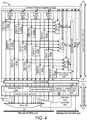
- FIG 3 is a schematic block diagram illustrating one embodiment 300 of a solid-state storage controller 104 with a write data pipeline 106 and a read data pipeline 108 in a solid-state storage device 102 in accordance with the present invention.
- the embodiment 300 includes a data bus 204, a local bus 206, and buffer control 208, which are substantially similar to those described in relation to the solid-state storage device controller 202 of Figure 2 .
- the write data pipeline 106 includes a packetizer 302 and an error-correcting code (“ECC”) generator 304.
- ECC error-correcting code
- the write data pipeline 106 includes an input buffer 306, a write synchronization buffer 308, a write program module 310, a compression module 312, an encryption module 314, a garbage collector bypass 316 (with a portion within the read data pipeline 108), a media encryption module 318, and a write buffer 320.
- the read data pipeline 108 includes a read synchronization buffer 328, an ECC correction module 322, a depacketizer 324, an alignment module 326, and an output buffer 330.
- the read data pipeline 108 may include a media decryption module 332, a portion of the garbage collector bypass 316, a decryption module 334, a decompression module 336, and a read program module 338.
- the solid-state storage controller 104 may also include control and status registers 340 and control queues 342, a bank interleave controller 344, a synchronization buffer 346, a storage bus controller 348, and a multiplexer ("MUX") 350.
- the components of the solid-state controller 104 and associated write data pipeline 106 and read data pipeline 108 are described below. In other embodiments, synchronous solid-state storage media 110 may be used and synchronization buffers 308 328 may be eliminated.
- the write data pipeline 106 includes a packetizer 302 that receives a data or metadata segment to be written to the solid-state storage, either directly or indirectly through another write data pipeline 106 stage, and creates one or more packets sized for the solid-state storage media 110.
- the data or metadata segment is typically part of a data structure such as an object, but may also include an entire data structure. In another embodiment, the data segment is part of a block of data, but may also include an entire block of data.
- a set of data such as a data structure is received from a computer such as the host 114, or other computer or device and is transmitted to the solid-state storage device 102 in data segments streamed to the solid-state storage device 102.
- a data segment may also be known by another name, such as data parcel, but as referenced herein includes all or a portion of a data structure or data block.
- Each data structure is stored as one or more packets.
- Each data structure may have one or more container packets.
- Each packet contains a header.
- the header may include a header type field. Type fields may include data, attribute, metadata, data segment delimiters (multi-packet), data structures, data linkages, and the like.
- the header may also include information regarding the size of the packet, such as the number of bytes of data included in the packet. The length of the packet may be established by the packet type.
- the header may include information that establishes the relationship of the packet to a data structure. An example might be the use of an offset in a data packet header to identify the location of the data segment within the data structure.
- One of skill in the art will recognize other information that may be included in a header added to data by a packetizer 302 and other information that may be added to a data packet.
- Each packet includes a header and possibly data from the data or metadata segment.
- the header of each packet includes pertinent information to relate the packet to the data structure to which the packet belongs.
- the header may include an object identifier or other data structure identifier and offset that indicates the data segment, object, data structure or data block from which the data packet was formed.
- the header may also include a logical address used by the storage bus controller 348 to store the packet.
- the header may also include information regarding the size of the packet, such as the number of bytes included in the packet.
- the header may also include a sequence number that identifies where the data segment belongs with respect to other packets within the data structure when reconstructing the data segment or data structure.
- the header may include a header type field.
- Type fields may include data, data structure attributes, metadata, data segment delimiters (multi-packet), data structure types, data structure linkages, and the like.
- data segment delimiters multi-packet
- data structure types data structure linkages, and the like.
- packetizer 302 One of skill in the art will recognize other information that may be included in a header added to data or metadata by a packetizer 302 and other information that may be added to a packet.
- the write data pipeline 106 includes an ECC generator 304 that that generates one or more error-correcting codes ("ECC") for the one or more packets received from the packetizer 302.
- ECC error-correcting codes
- the ECC generator 304 typically uses an error correcting algorithm to generate ECC check bits which are stored with the one or more data packets.
- the ECC codes generated by the ECC generator 304 together with the one or more data packets associated with the ECC codes comprise an ECC chunk.
- the ECC data stored with the one or more data packets is used to detect and to correct errors introduced into the data through transmission and storage.
- packets are streamed into the ECC generator 304 as un-encoded blocks of length N.
- a syndrome of length S is calculated, appended and output as an encoded block of length N+S.
- N and S are dependent upon the characteristics of the ECC algorithm which is selected to achieve specific performance, efficiency, and robustness metrics.
- the packet may comprise more than one ECC block; the ECC block may comprise more than one packet; and a first packet may end anywhere within the ECC block and a second packet may begin after the end of the first packet within the same ECC block.
- ECC algorithms are not dynamically modified.
- the ECC data stored with the data packets is robust enough to correct errors in more than two bits.
- the life of the solid-state storage media 110 allows the life of the solid-state storage media 110 to be extended.
- the flash memory may be written approximately 100,000 times without error per erase cycle. This usage limit may be extended using a robust ECC algorithm.
- the solid-state storage device 102 can internally correct errors and has a longer useful life than if a less robust ECC algorithm is used, such as single bit correction.
- the ECC generator 304 may use a less robust algorithm and may correct single-bit or double-bit errors.
- the solid-state storage device 110 may comprise less reliable storage such as multi-level cell (“MLC”) flash in order to increase capacity, which storage may not be sufficiently reliable without more robust ECC algorithms.
- MLC multi-level cell
- the write pipeline 106 includes an input buffer 306 that receives a data segment to be written to the solid-state storage media 110 and stores the incoming data segments until the next stage of the write data pipeline 106, such as the packetizer 302 (or other stage for a more complex write data pipeline 106) is ready to process the next data segment.
- the input buffer 306 typically allows for discrepancies between the rate data segments are received and processed by the write data pipeline 106 using an appropriately sized data buffer.
- the input buffer 306 also allows the data bus 204 to transfer data to the write data pipeline 106 at rates greater than can be sustained by the write data pipeline 106 in order to improve efficiency of operation of the data bus 204.
- a buffering function is performed elsewhere, such as in the solid-state storage device 102 but outside the write data pipeline 106, in the host 114, such as within a network interface card (“NIC”), or at another device, for example when using remote direct memory access (“RDMA").
- NIC network interface card
- RDMA remote direct memory access
- the write data pipeline 106 also includes a write synchronization buffer 308 that buffers packets received from the ECC generator 304 prior to writing the packets to the solid-state storage media 110.
- the write synchronization buffer 308 is located at a boundary between a local clock domain and a solid-state storage clock domain and provides buffering to account for the clock domain differences.
- synchronous solid-state storage media 110 may be used and synchronization buffers 308 328 may be eliminated.
- the write data pipeline 106 also includes a media encryption module 318 that receives the one or more packets from the packetizer 302, either directly or indirectly, and encrypts the one or more packets using an encryption key unique to the solid-state storage device 102 prior to sending the packets to the ECC generator 304.
- the entire packet is encrypted, including the headers.
- headers are not encrypted.
- encryption key is understood to mean a secret encryption key that is managed externally from a solid-state storage controller 104.
- the media encryption module 318 and corresponding media decryption module 332 provide a level of security for data stored in the solid-state storage media 110. For example, where data is encrypted with the media encryption module 318, if the solid-state storage media 110 is connected to a different solid-state storage controller 104, solid-state storage device 102, or server, the contents of the solid-state storage media 110 typically could not be read without use of the same encryption key used during the write of the data to the solid-state storage media 110 without significant effort.
- the solid-state storage device 102 does not store the encryption key in non-volatile storage and allows no external access to the encryption key.
- the encryption key is provided to the solid-state storage controller 104 during initialization.
- the solid-state storage device 102 may use and store a non-secret cryptographic nonce that is used in conjunction with an encryption key. A different nonce may be stored with every packet. Data segments may be split between multiple packets with unique nonces for the purpose of improving protection by the encryption algorithm.
- the encryption key may be received from a host 114, a server, key manager, or other device that manages the encryption key to be used by the solid-state storage controller 104.
- the solid-state storage media 110 may have two or more partitions and the solid-state storage controller 104 behaves as though it was two or more solid-state storage controllers 104, each operating on a single partition within the solid-state storage media 110.
- a unique media encryption key may be used with each partition.
- the write data pipeline 106 also includes an encryption module 314 that encrypts a data or metadata segment received from the input buffer 306, either directly or indirectly, prior sending the data segment to the packetizer 302, the data segment encrypted using an encryption key received in conjunction with the data segment.
- the encryption keys used by the encryption module 314 to encrypt data may not be common to all data stored within the solid-state storage device 102 but may vary on an per data structure basis and received in conjunction with receiving data segments as described below. For example, an encryption key for a data segment to be encrypted by the encryption module 314 may be received with the data segment or may be received as part of a command to write a data structure to which the data segment belongs.
- the solid-sate storage device 102 may use and store a non-secret cryptographic nonce in each data structure packet that is used in conjunction with the encryption key.
- a different nonce may be stored with every packet.
- Data segments may be split between multiple packets with unique nonces for the purpose of improving protection by the encryption algorithm.
- the encryption key may be received from a host 114, another computer, key manager, or other device that holds the encryption key to be used to encrypt the data segment.
- encryption keys are transferred to the solid-state storage controller 104 from one of a solid-state storage device 102, host 114, computer, or other external agent which has the ability to execute industry standard methods to securely transfer and protect private and public keys.
- the encryption module 314 encrypts a first packet with a first encryption key received in conjunction with the packet and encrypts a second packet with a second encryption key received in conjunction with the second packet. In another embodiment, the encryption module 314 encrypts a first packet with a first encryption key received in conjunction with the packet and passes a second data packet on to the next stage without encryption.
- the encryption module 314 included in the write data pipeline 106 of the solid-state storage device 102 allows data structure-by-data structure or segment-by-segment data encryption without a single file system or other external system to keep track of the different encryption keys used to store corresponding data structures or data segments.
- Each requesting device 155 or related key manager independently manages encryption keys used to encrypt only the data structures or data segments sent by the requesting device 155.
- the encryption module 314 may encrypt the one or more packets using an encryption key unique to the solid-state storage device 102.
- the encryption module 314 may perform this media encryption independently, or in addition to the encryption described above.
- the entire packet is encrypted, including the headers.
- headers are not encrypted.
- the media encryption by the encryption module 314 provides a level of security for data stored in the solid-state storage media 110.
- solid-state storage media 110 is connected to a different solid-state storage controller 104, solid-state storage device 102, or host 114, the contents of the solid-state storage media 110 typically could not be read without use of the same encryption key used during the write of the data to the solid-state storage media 110 without significant effort.
- the write data pipeline 106 includes a compression module 312 that compresses the data for metadata segment prior to sending the data segment to the packetizer 302.
- the compression module 312 typically compresses a data or metadata segment using a compression routine known to those of skill in the art to reduce the storage size of the segment. For example, if a data segment includes a string of 512 zeros, the compression module 312 may replace the 512 zeros with code or token indicating the 512 zeros where the code is much more compact than the space taken by the 512 zeros.
- the compression module 312 compresses a first segment with a first compression routine and passes along a second segment without compression. In another embodiment, the compression module 312 compresses a first segment with a first compression routine and compresses the second segment with a second compression routine. Having this flexibility within the solid-state storage device 102 is beneficial so that hosts 114 or other devices writing data to the solid-state storage device 102 may each specify a compression routine or so that one can specify a compression routine while another specifies no compression. Selection of compression routines may also be selected according to default settings on a per data structure type or data structure class basis.
- a first data structure of a specific data structure may be able to override default compression routine settings and a second data structure of the same data structure class and data structure type may use the default compression routine and a third data structure of the same data structure class and data structure type may use no compression.
- the write data pipeline 106 includes a garbage collector bypass 316 that receives data segments from the read data pipeline 108 as part of a data bypass in a garbage collection system.
- a garbage collection system typically marks packets that are no longer valid, typically because the packet is marked for deletion or has been modified and the modified data is stored in a different location.
- the garbage collection system determines that a particular section of storage may be recovered. This determination may be due to a lack of available storage capacity, the percentage of data marked as invalid reaching a threshold, a consolidation of valid data, an error detection rate for that section of storage reaching a threshold, or improving performance based on data distribution, etc. Numerous factors may be considered by a garbage collection algorithm to determine when a section of storage is to be recovered.
- the garbage collector bypass 316 allows packets to be read into the read data pipeline 108 and then transferred directly to the write data pipeline 106 without being routed out of the solid-state storage controller 104.
- the garbage collector bypass 316 is part of an autonomous garbage collector system that operates within the solid-state storage device 102. This allows the solid-state storage device 102 to manage data so that data is systematically spread throughout the solid-state storage media 110 to improve performance, data reliability and to avoid overuse and underuse of any one location or area of the solid-state storage media 110 and to lengthen the useful life of the solid-state storage media 110.
- the garbage collector bypass 316 coordinates insertion of segments into the write data pipeline106 with other segments being written by hosts 114 or other devices.
- the garbage collector bypass 316 is before the packetizer 302 in the write data pipeline 106 and after the depacketizer 324 in the read data pipeline 108, but may also be located elsewhere in the read and write data pipelines 106, 108.
- the garbage collector bypass 316 may be used during a flush of the write pipeline 108 to fill the remainder of the logical page in order to improve the efficiency of storage within the solid-state storage media 110 and thereby reduce the frequency of garbage collection.
- the write data pipeline 106 includes a write buffer 320 that buffers data for efficient write operations.
- the write buffer 320 includes enough capacity for packets to fill at least one logical page in the solid-state storage media 110. This allows a write operation to send an entire page of data to the solid-state storage media 110 without interruption.
- the solid-state storage media 110 may be used for other read operations. This is advantageous because other solid-state devices with a smaller write buffer or no write buffer may tie up the solid-state storage when data is written to a storage write buffer and data flowing into the storage write buffer stalls. Read operations will be blocked until the entire storage write buffer is filled and programmed.
- Another approach for systems without a write buffer or a small write buffer is to flush the storage write buffer that is not full in order to enable reads. Again this is inefficient because multiple write/program cycles are required to fill a page.
- a single write command which includes numerous subcommands, can then be followed by a single program command to transfer the page of data from the storage write buffer in each solid-state storage element 216, 218, 220 to the designated page within each solid-state storage element 216, 218, 220.
- This technique has the benefits of eliminating partial page programming, which is known to reduce data reliability and durability and freeing up the destination bank for reads and other commands while the buffer fills.
- the write buffer 320 is a ping-pong buffer where one side of the buffer is filled and then designated for transfer at an appropriate time while the other side of the ping-pong buffer is being filled.
- the write buffer 320 includes a first-in first-out ("FIFO") register with a capacity of more than a logical page of data segments.
- FIFO first-in first-out
- the write buffer 320 is sized smaller than a logical page so that less than a page of information could be written to a storage write buffer in the solid-state storage media 110.
- data is queued using the garbage collection system that needs to be moved from one location to another as part of the garbage collection process.
- the data can be fed through the garbage collector bypass 316 to the write buffer 320 and then on to the storage write buffer in the solid-state storage media 110 to fill the pages of a logical page prior to programming the data. In this way a data stall in the write data pipeline 106 would not stall reading from the solid-state storage device 102.
- the write data pipeline 106 includes a write program module 310 with one or more user-definable functions within the write data pipeline 106.
- the write program module 310 allows a user to customize the write data pipeline 106.
- a user may customize the write data pipeline 106 based on a particular data requirement or application.
- the solid-state storage controller 104 is an FPGA
- the user may program the write data pipeline 106 with custom commands and functions relatively easily.
- a user may also use the write program module 310 to include custom functions with an ASIC, however, customizing an ASIC may be more difficult than with an FPGA.
- the write program module 310 may include buffers and bypass mechanisms to allow a first data segment to execute in the write program module 310 while a second data segment may continue through the write data pipeline 106.
- the write program module 310 may include a processor core that can be programmed through software.
- write program module 310 is shown between the input buffer 306 and the compression module 312, however, the write program module 310 could be anywhere in the write data pipeline 106 and may be distributed among the various stages 302-320. In addition, there may be multiple write program modules 310 distributed among the various states 302-320 that are programmed and operate independently. In addition, the order of the stages 302-320 may be altered. One of skill in the art will recognize workable alterations to the order of the stages 302-320 based on particular user requirements.
- the read data pipeline 108 includes an ECC correction module 322 that determines if a data error exists in ECC blocks a requested packet received from the solid-state storage media 110 by using ECC stored with each ECC block of the requested packet. The ECC correction module 322 then corrects any errors in the requested packet if any error exists and the errors are correctable using the ECC. For example, if the ECC can detect an error in six bits but can only correct three bit errors, the ECC correction module 322 corrects ECC blocks of the requested packet with up to three bits in error. The ECC correction module 322 corrects the bits in error by changing the bits in error to the correct one or zero state so that the requested data packet is identical to when it was written to the solid-state storage media 110 and the ECC was generated for the packet.
- the ECC correction module 322 determines that the requested packets contains more bits in error than the ECC can correct, the ECC correction module 322 cannot correct the errors in the corrupted ECC blocks of the requested packet and sends an interrupt.
- the ECC correction module 322 sends an interrupt with a message indicating that the requested packet is in error.
- the message may include information that the ECC correction module 322 cannot correct the errors or the inability of the ECC correction module 322 to correct the errors may be implied.
- the ECC correction module 322 sends the corrupted ECC blocks of the requested packet with the interrupt and/or the message.
- a corrupted ECC block or portion of a corrupted ECC block of the requested packet that cannot be corrected by the ECC correction module 322 is read by the master controller 224, corrected, and returned to the ECC correction module 322 for further processing by the read data pipeline 108.
- a corrupted ECC block or portion of a corrupted ECC block of the requested packet is sent to the device requesting the data.
- the requesting device 155 may correct the ECC block or replace the data using another copy, such as a backup or mirror copy, and then may use the replacement data of the requested data packet or return it to the read data pipeline 108.
- the requesting device 155 may use header information in the requested packet in error to identify data required to replace the corrupted requested packet or to replace the data structure to which the packet belongs.
- the solid-state storage controller 104 stores data using some type of RAID and is able to recover the corrupted data.
- the ECC correction module 322 sends an interrupt and/or message and the receiving device fails the read operation associated with the requested data packet.
- One of skill in the art will recognize other options and actions to be taken as a result of the ECC correction module 322 determining that one or more ECC blocks of the requested packet are corrupted and that the ECC correction module 322 cannot correct the errors.
- the read data pipeline 108 includes a depacketizer 324 that receives ECC blocks of the requested packet from the ECC correction module 322, directly or indirectly, and checks and removes one or more packet headers.
- the depacketizer 324 may validate the packet headers by checking packet identifiers, data length, data location, etc. within the headers.
- the header includes a hash code that can be used to validate that the packet delivered to the read data pipeline 108 is the requested packet.
- the depacketizer 324 also removes the headers from the requested packet added by the packetizer 302.
- the depacketizer 324 may directed to not operate on certain packets but pass these forward without modification.
- An example might be a container label that is requested during the course of a rebuild process where the header information is required for index reconstruction. Further examples include the transfer of packets of various types destined for use within the solid-state storage device 102. In another embodiment, the depacketizer 324 operation may be packet type dependent.
- the read data pipeline 108 includes an alignment module 326 that receives data from the depacketizer 324 and removes unwanted data.
- a read command sent to the solid-state storage media 110 retrieves a packet of data.
- a device requesting the data may not require all data within the retrieved packet and the alignment module 326 removes the unwanted data. If all data within a retrieved page is requested data, the alignment module 326 does not remove any data.
- the alignment module 326 re-formats the data as data segments of a data structure in a form compatible with a device requesting the data segment prior to forwarding the data segment to the next stage.
- the alignment module 326 uses received data to format the data into data segments suitable to be sent to the requesting device 155 and joined to form a response. For example, data from a portion of a first data packet may be combined with data from a portion of a second data packet. If a data segment is larger than a data requested by the requesting device 155, the alignment module 326 may discard the unwanted data.
- the read data pipeline 108 includes a read synchronization buffer 328 that buffers one or more requested packets read from the solid-state storage media 110 prior to processing by the read data pipeline 108.
- the read synchronization buffer 328 is at the boundary between the solid-state storage clock domain and the local bus clock domain and provides buffering to account for the clock domain differences.
- the read data pipeline 108 includes an output buffer 330 that receives requested packets from the alignment module 326 and stores the packets prior to transmission to the requesting device 155.
- the output buffer 330 accounts for differences between when data segments are received from stages of the read data pipeline 108 and when the data segments are transmitted to other parts of the solid-state storage controller 104 or to the requesting device 155.
- the output buffer 330 also allows the data bus 204 to receive data from the read data pipeline 108 at rates greater than can be sustained by the read data pipeline 108 in order to improve efficiency of operation of the data bus 204.
- the read data pipeline 108 includes a media decryption module 332 that receives one or more encrypted requested packets from the ECC correction module 322 and decrypts the one or more requested packets using the encryption key unique to the solid-state storage device 102 prior to sending the one or more requested packets to the depacketizer 324.
- the encryption key used to decrypt data by the media decryption module 332 is identical to the encryption key used by the media encryption module 318.
- the solid-state storage media 110 may have two or more partitions and the solid-state storage controller 104 behaves as though it was two or more solid-state storage controllers 104 each operating on a single partition within the solid-state storage media 110. In this embodiment, a unique media encryption key may be used with each partition.
- the read data pipeline 108 includes a decryption module 334 that decrypts a data segment formatted by the depacketizer 324 prior to sending the data segment to the output buffer 330.
- the data segment may be decrypted using an encryption key received in conjunction with the read request that initiates retrieval of the requested packet received by the read synchronization buffer 328.
- the decryption module 334 may decrypt a first packet with an encryption key received in conjunction with the read request for the first packet and then may decrypt a second packet with a different encryption key or may pass the second packet on to the next stage of the read data pipeline 108 without decryption.
- the nonce When the packet was stored with a non-secret cryptographic nonce, the nonce is used in conjunction with an encryption key to decrypt the data packet.
- the encryption key may be received from a host 114, a computer, key manager, or other device that manages the encryption key to be used by the solid-state storage controller 104.
- the read data pipeline 108 includes a decompression module 336 that decompresses a data segment formatted by the depacketizer 324.
- the decompression module 336 uses compression information stored in one or both of the packet header and the container label to select a complementary routine to that used to compress the data by the compression module 312.
- the decompression routine used by the decompression module 336 is dictated by the device requesting the data segment being decompressed.
- the decompression module 336 selects a decompression routine according to default settings on a per data structure type or data structure class basis.
- a first packet of a first object may be able to override a default decompression routine and a second packet of a second data structure of the same data structure class and data structure type may use the default decompression routine and a third packet of a third data structure of the same data structure class and data structure type may use no decompression.
- the read data pipeline 108 includes a read program module 338 that includes one or more user-definable functions within the read data pipeline 108.
- the read program module 338 has similar characteristics to the write program module 310 and allows a user to provide custom functions to the read data pipeline 108.
- the read program module 338 may be located as shown in Figure 3 , may be located in another position within the read data pipeline 108, or may include multiple parts in multiple locations within the read data pipeline 108. Additionally, there may be multiple read program modules 338 within multiple locations within the read data pipeline 108 that operate independently.
- One of skill in the art will recognize other forms of a read program module 338 within a read data pipeline 108.
- the stages of the read data pipeline 108 may be rearranged and one of skill in the art will recognize other orders of stages within the read data pipeline 108.
- the solid-state storage controller 104 includes control and status registers 340 and corresponding control queues 342.
- the control and status registers 340 and control queues 342 facilitate control and sequencing commands and subcommands associated with data processed in the write and read data pipelines 106, 108.
- a data segment in the packetizer 302 may have one or more corresponding control commands or instructions in a control queue 342 associated with the ECC generator 304.
- As the data segment is packetized, some of the instructions or commands may be executed within the packetizer 302. Other commands or instructions may be passed to the next control queue 342 through the control and status registers 340 as the newly formed data packet created from the data segment is passed to the next stage.
- Commands or instructions may be simultaneously loaded into the control queues 342 for a packet being forwarded to the write data pipeline 106 with each pipeline stage pulling the appropriate command or instruction as the respective packet is executed by that stage.
- commands or instructions may be simultaneously loaded into the control queues 342 for a packet being requested from the read data pipeline 108 with each pipeline stage pulling the appropriate command or instruction as the respective packet is executed by that stage.
- One of skill in the art will recognize other features and functions of control and status registers 340 and control queues 342.
- the solid-state storage controller 104 and or solid-state storage device 102 may also include a bank interleave controller 344, a synchronization buffer 346, a storage bus controller 348, and a multiplexer (“MUX") 350, which are described in relation to Figure 4 .
- MUX multiplexer
- FIG. 4 is a schematic block diagram illustrating one embodiment 400 of a bank interleave controller 344 in the solid-state storage controller 104 in accordance with the present invention.
- the bank interleave controller 344 is connected to the control and status registers 340 and to the storage I/O bus 210 and storage control bus 212 through the MUX 350, storage bus controller 348, and synchronization buffer 346, which are described below.
- the bank interleave controller 344 includes a read agent 402, a write agent 404, an erase agent 406, a management agent 408, read queues 410a-n, write queues 412a-n, erase queues 414a-n, and management queues 416a-n for the banks 214 in the solid-state storage media 110, bank controllers 418a-n, a bus arbiter 420, and a status MUX 422, which are described below.
- the storage bus controller 348 includes a mapping module 424 with a remapping module 430, a status capture module 426, and a NAND bus controller 428, which are described below.
- the bank interleave controller 344 directs one or more commands to two or more queues in the bank interleave controller 104 and coordinates among the banks 214 of the solid-state storage media 110 execution of the commands stored in the queues, such that a command of a first type executes on one bank 214a while a command of a second type executes on a second bank 214b.
- the one or more commands are separated by command type into the queues.
- Each bank 214 of the solid-state storage media 110 has a corresponding set of queues within the bank interleave controller 344 and each set of queues includes a queue for each command type.
- the bank interleave controller 344 coordinates among the banks 214 of the solid-state storage media 110 execution of the commands stored in the queues. For example, a command of a first type executes on one bank 214a while a command of a second type executes on a second bank 214b.
- the command types and queue types include read and write commands and queues 410, 412, but may also include other commands and queues that are storage media specific.
- erase and management queues 414, 416 are included and would be appropriate for flash memory, NRAM, MRAM, DRAM, PRAM, etc.
- solid-state storage media 110 For other types of solid-state storage media 110, other types of commands and corresponding queues may be included without straying from the scope of the invention.
- the flexible nature of an FPGA solid-state storage controller 104 allows flexibility in storage media. If flash memory were changed to another solid-state storage type, the bank interleave controller 344, storage bus controller 348, and MUX 350 could be altered to accommodate the media type without significantly affecting the data pipelines 106, 108 and other solid-state storage controller 104 functions.
- the bank interleave controller 344 includes, for each bank 214, a read queue 410 for reading data from the solid-state storage media 110, a write queue 412 for write commands to the solid-state storage media 110, an erase queue 414 for erasing an erase block in the solid-state storage, an a management queue 416 for management commands.
- the bank interleave controller 344 also includes corresponding read, write, erase, and management agents 402, 404, 406, 408.
- the control and status registers 340 and control queues 342 or similar components queue commands for data sent to the banks 214 of the solid-state storage media 110 without a bank interleave controller 344.
- the agents 402, 404, 406, 408, in one embodiment, direct commands of the appropriate type destined for a particular bank 214a to the correct queue for the bank 214a.
- the read agent 402 may receive a read command for bank-1 214b and directs the read command to the bank-1 read queue 410b.
- the write agent 404 may receive a write command to write data to a location in bank-0 214a of the solid-state storage media 110 and will then send the write command to the bank-0 write queue 412a.
- the erase agent 406 may receive an erase command to erase an erase block in bank-1 214b and will then pass the erase command to the bank-1 erase queue 414b.
- the management agent 408 typically receives management commands, status requests, and the like, such as a reset command or a request to read a configuration register of a bank 214, such as bank-0 214a.
- the management agent 408 sends the management command to the bank-0 management queue 416a.
- the agents 402, 404, 406, 408 typically also monitor status of the queues 410, 412, 414, 416 and send status, interrupt, or other messages when the queues 410, 412, 414, 416 are full, nearly full, non-functional, etc.
- the agents 402, 404, 406, 408 receive commands and generate corresponding sub-commands.
- the agents 402, 404, 406, 408 receive commands through the control & status registers 340 and generate corresponding sub-commands which are forwarded to the queues 410, 412, 414, 416.
- One of skill in the art will recognize other functions of the agents 402, 404, 406, 408.
- the queues 410, 412, 414, 416 typically receive commands and store the commands until required to be sent to the solid-state storage banks 214.
- the queues 410, 412, 414, 416 are first-in, first-out ("FIFO") registers or a similar component that operates as a FIFO.
- the queues 410, 412, 414, 416 store commands in an order that matches data, order of importance, or other criteria.
- the bank controllers 418 typically receive commands from the queues 410, 412, 414, 416 and generate appropriate subcommands.
- the bank-0 write queue 412a may receive a command to write a page of data packets to bank-0 214a.
- the bank-0 controller 418a may receive the write command at an appropriate time and may generate one or more write subcommands for each data packet stored in the write buffer 320 to be written to the page in bank-0 214a.
- bank-0 controller 418a may generate commands to validate the status of bank 0 214a and the solid-state storage array 216, select the appropriate location for writing one or more data packets, clear the input buffers within the solid-state storage memory array 216, transfer the one or more data packets to the input buffers, program the input buffers into the selected location, verify that the data was correctly programmed, and if program failures occur do one or more of interrupting the master controller 224, retrying the write to the same physical location, and retrying the write to a different physical location.
- the storage bus controller 348 will cause the one or more commands to multiplied to each of the each of the storage I/O buses 210a-n with the logical address of the command mapped to a first physical addresses for storage I/O bus 210a, and mapped to a second physical address for storage I/O bus 210b, and so forth as further described below.
- bus arbiter 420 selects from among the bank controllers 418 and pulls subcommands from output queues within the bank controllers 418 and forwards these to the Storage Bus Controller 348 in a sequence that optimizes the performance of the banks 214.
- the bus arbiter 420 may respond to a high level interrupt and modify the normal selection criteria.
- the master controller 224 can control the bus arbiter 420 through the control and status registers 340.
- One of skill in the art will recognize other means by which the bus arbiter 420 may control and interleave the sequence of commands from the bank controllers 418 to the solid-state storage media 110.
- the bus arbiter 420 typically coordinates selection of appropriate commands, and corresponding data when required for the command type, from the bank controllers 418 and sends the commands and data to the storage bus controller 348.
- the bus arbiter 420 typically also sends commands to the storage control bus 212 to select the appropriate bank 214.
- only one command (control information) or set of data can be transmitted at a time.
- write commands or data are being transmitted to the solid-state storage media 110 on the storage I/O bus 210
- read commands, data being read, erase commands, management commands, or other status commands cannot be transmitted on the storage I/O bus 210.
- data cannot be written to the solid-state storage media 110.
- the bus arbiter 420 selects the bank-0 controller 418a which may have a write command or a series of write sub-commands on the top of its queue which cause the storage bus controller 348 to execute the following sequence.
- the bus arbiter 420 forwards the write command to the storage bus controller 348, which sets up a write command by selecting bank-0 214a through the storage control bus 212, sending a command to clear the input buffers of the solid-state storage elements 110 associated with the bank-0 214a, and sending a command to validate the status of the solid-state storage elements 216, 218, 220 associated with the bank-0 214a.
- the storage bus controller 348 then transmits a write subcommand on the storage I/O bus 210, which contains the physical addresses including the address of the logical erase block for each individual physical erase solid-stage storage element 216a-m as mapped from the logical erase block address.
- the storage bus controller 348 then muxes the write buffer 320 through the write synchronization buffer 308 to the storage I/O bus 210 through the MUX 350 and streams write data to the appropriate page.
- storage bus controller 348 causes the solid-state storage elements 216a-m associated with the bank-0 214a to program the input buffer to the memory cells within the solid-state storage elements 216a-m.
- the storage bus controller 348 validates the status to ensure that page was correctly programmed.
- a read operation is similar to the write example above.
- the bus arbiter 420 or other component of the bank interleave controller 344, receives data and corresponding status information and sends the data to the read data pipeline 108 while sending the status information on to the control and status registers 340.
- a read data command forwarded from bus arbiter 420 to the storage bus controller 348 will cause the MUX 350 to gate the read data on storage I/O bus 210 to the read data pipeline 108 and send status information to the appropriate control and status registers 340 through the status MUX 422.
- the bus arbiter 420 coordinates the various command types and data access modes so that only an appropriate command type or corresponding data is on the bus at any given time. If the bus arbiter 420 has selected a write command, and write subcommands and corresponding data are being written to the solid-state storage media 110, the bus arbiter 420 will not allow other command types on the storage I/O bus 210. Beneficially, the bus arbiter 420 uses timing information, such as predicted command execution times, along with status information received concerning bank 214 status to coordinate execution of the various commands on the bus with the goal of minimizing or eliminating idle time of the busses.
- the master controller 224 through the bus arbiter 420 typically uses expected completion times of the commands stored in the queues 410, 412, 414, 416, along with status information, so that when the subcommands associated with a command are executing on one bank 214a, other subcommands of other commands are executing on other banks 214b-n.
- the bus arbiter 420 directs another command to the bank 214a.
- the bus arbiter 420 may also coordinate commands stored in the queues 410, 412, 414, 416 with other commands that are not stored in the queues 410, 412, 414,416.
- an erase command may be sent out to erase a group of erase blocks within the solid-state storage media 110.
- An erase command may take 10 to 1000 times more time to execute than a write or a read command or 10 to 100 times more time to execute than a program command.
- the bank interleave controller 344 may split the erase command into N commands, each to erase a virtual erase block of a bank 214a. While Bank 0 214a is executing an erase command, the bus arbiter 420 may select other commands for execution on the other banks 214b-n.
- the bus arbiter 420 may also work with other components, such as the storage bus controller 348, the master controller 224, etc., to coordinate command execution among the buses.
- the solid-state controller 104 includes one bank interleave controller 344 that serves all of the storage elements 216, 218, 220 of the solid-state storage media 110.
- the solid-state controller 104 includes a bank interleave controller 344 for each column of storage elements 216a-m, 218a-m, 220a-m.
- one bank interleave controller 344 serves one column of storage elements SSS 0.0-SSS N.0 216a, 218a,... 220a
- a second bank interleave controller 344 serves a second column of storage elements SSS 0.1-SSS N.1 216b, 218b,... 220b etc.
- the solid-state storage controller 104 includes a synchronization buffer 346 that buffers commands and status messages sent and received from the solid-state storage media 110.
- the synchronization buffer 346 is located at the boundary between the solid-state storage clock domain and the local bus clock domain and provides buffering to account for the clock domain differences.
- the synchronization buffer 346, write synchronization buffer 308, and read synchronization buffer 328 may be independent or may act together to buffer data, commands, status messages, etc.
- the synchronization buffer 346 is located where there are the fewest number of signals crossing the clock domains.
- synchronization between clock domains may be arbitrarily moved to other locations within the solid-state storage device 102 in order to optimize some aspect of design implementation.
- the solid-state storage controller 104 includes a storage bus controller 348 that interprets and translates commands for data sent to and read from the solid-state storage media 110 and status messages received from the solid-state storage media 110 based on the type of solid-state storage media 110.
- the storage bus controller 348 may have different timing requirements for different types of storage, storage with different performance characteristics, storage from different manufacturers, etc.
- the storage bus controller 348 also sends control commands to the storage control bus 212.
- the solid-state storage controller 104 includes a MUX 350 that comprises an array of multiplexers 350a-n where each multiplexer is dedicated to a row in the solid-state storage array 110.
- multiplexer 350a is associated with solid-state storage elements 216a, 218a, 220a.
- MUX 350 routes the data from the write data pipeline 106 and commands from the storage bus controller 348 to the solid-state storage media 110 via the storage I/O bus 210 and routes data and status messages from the solid-state storage media 110 via the storage I/O bus 210 to the read data pipeline 108 and the control and status registers 340 through the storage bus controller 348, synchronization buffer 346, and bank interleave controller 344.
- the solid-state storage controller 104 includes a MUX 350 for each column of solid-state storage elements (e.g. SSS 0.0 216a, SSS 1.0 218a, SSS N.0 220a).
- a MUX 350 combines data from the write data pipeline 106 and commands sent to the solid-state storage media 110 via the storage I/O bus 210 and separates data to be processed by the read data pipeline 108 from commands.
- Packets stored in the write buffer 320 are directed on busses out of the write buffer 320 through a write synchronization buffer 308 for each column of solid-state storage elements (SSS 0.x to SSS N.x 216, 218, 220) to the MUX 350 for each column of solid-state storage elements (SSS 0.x to SSS N.x 216, 218, 220).
- the commands and read data are received by the MUXes 350 from the storage I/O bus 210.
- the MUXes 350 also direct status messages to the storage bus controller 348.
- the storage bus controller 348 includes a mapping module 424.
- the mapping module 424 maps a logical address of an erase block to one or more physical addresses of an erase block.
- a solid-state storage media 110 with an array of twenty storage elements (e.g. SSS 0.0 to SSS 0.M 216) per bank 214a may have a logical address for a particular erase block mapped to twenty physical addresses of the erase block, one physical address per storage element. Because the storage elements are accessed in parallel, erase blocks at the same position in each storage element in a column of storage elements 216a, 218a, 220a will share a physical address.
- To select one erase block (e.g. in storage element SSS 0.0 216a) instead of all erase blocks in the row (e.g. in storage elements SSS 0.0, 1.0, ... N.0 216a, 218a, 220a) instead of all erase blocks in the row (e.g. in storage elements SSS 0.0, 1.0, ... N.0 216a, 2
- the remapping module 430 changes a mapping of a logical address of an erase block to one or more physical addresses of a virtual erase block (spread over the array of storage elements).
- virtual erase block 1 may be mapped to erase block 1 of storage element SSS 0.0 216a, to erase block 1 of storage element SSS 0.1 216b, ..., and to storage element 0.M 216m
- virtual erase block 2 may be mapped to erase block 2 of storage element SSS 1.0 218a, to erase block 2 of storage element SSS 1.1 218b, ..., and to storage element 1.M 218m, etc.
- virtual erase block 1 may be mapped to one erase block from each storage element in an array such that virtual erase block 1 includes erase block 1 of storage element SSS 0.0 216a to erase block 1 of storage element SSS 0.1 216b to storage element 0.M 216m, and erase block 1 of storage element SSS 1.0 218a to erase block 1 of storage element SSS 1.1 218b, ..., and to storage element 1.M 218m, for each storage element in the array up to erase block 1 of storage element N.M 220m.
- the remapping module 430 could change the logical-to-physical mapping for the logical address that pointed to erase block 1 of virtual erase block 1. If a spare erase block (call it erase block 221) of storage element SSS 0.0 216a is available and currently not mapped, the remapping module 430 could change the mapping of virtual erase block 1 to point to erase block 221 of storage element SSS 0.0 216a, while continuing to point to erase block 1 of storage element SSS 0.1 216b, erase block 1 of storage element SSS 0.2 (not shown) ..., and to storage element 0.M 216m.
- the mapping module 424 or remapping module 430 could map erase blocks in a prescribed order (virtual erase block 1 to erase block 1 of the storage elements, virtual erase block 2 to erase block 2 of the storage elements, etc.) or may map erase blocks of the storage elements 216, 218, 220 in another order based on some other criteria.
- the erase blocks could be grouped by access time. Grouping by access time, meaning time to execute a command, such as programming (writing) data into pages of specific erase blocks, can level command completion so that a command executed across the erase blocks of a virtual erase block is not limited by the slowest erase block.
- the erase blocks may be grouped by wear level, health, etc.
- One of skill in the art will recognize other factors to consider when mapping or remapping erase blocks.
- the storage bus controller 348 includes a status capture module 426 that receives status messages from the solid-state storage media 110 and sends the status messages to the status MUX 422.
- the storage bus controller 348 when the solid-state storage media 110 is flash memory, the storage bus controller 348 includes a NAND bus controller 428.
- the NAND bus controller 428 directs commands from the read and write data pipelines 106, 108 to the correct location in the solid-state storage media 110, coordinates timing of command execution based on characteristics of the flash memory, etc. If the solid-state storage media 110 is another solid-state storage type, the NAND bus controller 428 would be replaced by a bus controller specific to the storage type.
- One of skill in the art will recognize other functions of a NAND bus controller 428.
- Figure 5A shows one embodiment of a power management apparatus 122.
- the power management apparatus 122 may include a monitor module 510 and a power loss module 520.
- the power loss module 520 includes an identification module 512, a terminate module 514, a corruption module 516, and a completion module 518.
- the monitor module 510 initiates a power loss mode in the nonvolatile storage device 102 in response to a primary power source failing to supply electric power above a predefined threshold through the primary power connection 130.
- the power loss mode in one embodiment, is a mode of operation in which the power management apparatus 122 prepares the storage device 102 for shutting down within a power hold-up time provided by the secondary power supply 124.
- the power loss module 520 in one embodiment, adjusts execution of in-process operations on the nonvolatile storage device 102 during the power loss mode, to allow essential in-process operations to execute.
- power above the predefined threshold is sufficient for the storage device 102.
- Sufficient power in one embodiment, is power that meets the requirements for the storage device 102 to operate properly.
- the predefined threshold in a further embodiment, is set at or above an insufficient power level for the storage device 102. Insufficient power is power that does not meet the requirements for the storage device 102. Power with a high AC or harmonic component when DC is expected and a voltage or current level that is too low are examples of insufficient power.
- the storage device 102 is configured to automatically accept or otherwise draw power from the secondary power supply 124 when power from the primary power source falls below the predefined threshold.
- the predefined threshold in one embodiment, is an engineered threshold determined by characteristics of the secondary power supply 124 and corresponding circuits.
- the primary power source in one embodiment, is a source of power that the nonvolatile storage device 102 uses during normal operation and which provides a substantially continuous supply of power that is not unexpectedly interrupted during normal operation.
- the computer system i.e. the host 114 or the like
- the primary power source provides power through the motherboard, such as through a bus or slot connection such as PCI, PCIe, AGP, or the like, or through an external port such as a USB port, a FireWire port, an eSATAp port, or the like.
- the primary power source is a standard electrical outlet.
- the monitor module 510 monitors the primary power connection 130 directly to determine when electric power from the primary power source falls below the predefined threshold.
- the monitor module 510 may include a power sensor, a current sensor, and/or another appropriate sensor to use to determine whether the nonvolatile storage device 102 is receiving sufficient external power.
- the monitor module 510 may be notified by another component in the nonvolatile storage device 102 in the event the nonvolatile storage device 102 loses external power.
- the monitor module 510 includes an analog circuit that responds to a loss of power from the primary power connection 130.
- the primary power connection 130 and the secondary power supply 124 may be placed in parallel such that the primary power connection 130 keeps the secondary power supply 124 fully charged (for example, when the secondary power supply 124 is made up of capacitors) and also supplies power to the storage device 102.
- the secondary power supply 124 naturally begins providing power in the event of a failure of the primary power connection 130, and the storage device 102 naturally accepts the power from the secondary power supply 124.
- the monitor module 510 circuit may also provide proper isolation to ensure that power from the secondary power supply 124 is sent to the storage device 102; for example, a diode may be used to ensure that, in the event of a failure in the primary power supply, power flows from the secondary power supply 124 to the storage device 102, and not to the failed primary power supply. Approaches to proper isolation will be appreciated by those of skill in the art in light of this disclosure.
- the monitor module 510 may still include detection components (such as current sensors, voltage sensors, or the like) to sense the power disruption and to initiate the power loss mode to trigger the operations of other modules in the power management apparatus 122 in response.
- monitor module 510 may sense a power disruption signal and activate a switch that changes the power draw for the storage device 102 from the primary power connection 130 to the secondary power supply 124, or the like.
- the monitor module 510 may initiate the power loss mode by directly or indirectly communicating to the power loss module 520 and/or another module that the storage device 102 has entered the power loss mode.
- the monitor module 122 may set a status register, send a power loss mode command, send a power loss signal, send a power loss interrupt, initiate a power loss mode function or procedure, place the storage device in a power loss state, and/or otherwise notify the power loss module 520 of the power loss mode.
- the power loss module 520 adjusts execution of in-process operations on the storage device 102 during the power loss mode, to ensure that essential operations, such as operations acknowledged to the host 114 or the like, are executed during the power hold-up time.
- In-process operations include operations that the storage device 102 is currently executing.
- in-process operations include operations that are queued for execution on the storage device 102, that are in-flight in the write data pipeline 106 and/or the read data pipeline 108, or the like.
- the power loss module 520 includes the identification module 512, the terminate module 514, and the corruption module 516.
- the identification module 512 identifies one or more non-essential operations on the nonvolatile storage device 102 in response to the monitor module 510 determining that external power has been lost, is below the predefined threshold, or is otherwise insufficient and entering the power loss mode.
- Non-essential operations are those operations that can be terminated, stopped, or paused, without causing data corruption or data loss on the storage device 102.
- Essential operations are those operations that must be executed in order to avoid data corruption, data loss on the storage device 102, or inconsistent communications between the storage device 102 and the host 114 (i.e. sending an acknowledgement to the host 114 for data that later is not properly handled consistent with the acknowledgement).
- the identification module 512 may further determine whether the non-essential operations are executing, or whether they are queued and awaiting execution.
- the terminate module 514 terminates the non-essential operations identified by the identification module 512.
- the terminate module 514 may terminate non-essential operations by erasing the non-essential operations, commands, and instructions that are queued and/or by interrupting non-essential operations that are currently executing on the storage device 102.
- the terminate module 514 allows the storage device 102 to power off (i.e. once the power hold-up time has expired and the secondary power supply 124 is depleted) without executing the non-essential operations.
- the terminate module 514 terminates the non-essential operations in a way that the non-essential operations are not executed or resumed once the storage device 102 is again powered on after a power loss. For example, in one embodiment, the terminate module 514 terminates the non-essential operations without leaving a record of the terminated non-essential operations, so that the storage device 102 powers on without executing or resuming the terminated non-essential operations.
- the identification module 512 also manages a power budget for the storage device 102 while the storage device 102 is operating on the secondary power supply 124.
- the identification module 512 may determine, for example, how much power is available, how much power all pending operations on the storage device 102 will require, and prioritize the pending operations. The operations may thus be reordered and executed in order of priority, to execute at least the essential in-process operations within the power hold-up time.
- the identification module 512 may log this information to provide notification, possibly after power is restored, to a user or system that some or all of the write operations have been lost.
- the non-essential operations include erase operations that are erasing nonvolatile memory 110 on the nonvolatile storage device 102 and/or read operations that are reading data on the nonvolatile storage device 102.
- the erase operations may have been generated, for example, as part of a garbage collection operation that is reclaiming space on a solid state storage device such as a Flash memory device.
- Non-essential operations may also include operations such as generating a hash key for data in the nonvolatile storage device 102, decompressing data read from storage, or other operations.
- Non-essential operations in a further embodiment, may include write (or program) operations for which the nonvolatile storage device 102 has not sent an acknowledgement to the host 114.
- a user or system designer specifies which operations are essential and which operations are non-essential.
- the terminate module 514 terminates the non-essential operations based on how much power they require. For example, erase operations in solid state storage devices tend to consume considerable amounts of power. The terminate module 514 may quickly terminate the erase operations in order to conserve power. In contrast, read operations require relatively little power. The terminate module 514 may begin terminating read operations only after the erase operations are terminated, or the like.
- the identification module 512 prioritizes operations, with the priorities based on the importance of executing the operation. For example, program operations for data that has been acknowledged may be given the highest priority, while an erase operation is given the lowest priority.
- the terminate module 514 may begin terminating the lowest priority operations and move up a prioritized list of operations, and not terminate any essential operations. Thus, the terminate module 514, beginning with the lowest priority operation, determines if the operation is essential. If not, that operation is terminated. If the operation is essential, the operation is not terminated and the terminate module 514 moves to the next operation for consideration.
- the identification module 512 may also prioritize non-essential operations that are in the process of executing based on the amount of energy required to complete the non-essential operation. For example, an erase operation that is 90% complete may be given a lower priority for termination than an erase operation that is 5% complete; thus, the erase operation that is 90% may be allowed to complete, while the erase operation that is 5% complete when the power disruption is detected is stopped. In one embodiment, the amount of energy required for an operation may vary over the time during which the operation is executed.
- the terminate module 514 terminates non-essential operations identified by the identification module 512.
- the terminate module 514 may terminate certain classes of operations (such as power-intensive erase operations or autonomous grooming operations), as prioritized by the identification module 512, for termination before other operations.
- the terminate module 514 terminates the non-essential operation by identifying the memory area or component on which the operation is working/executing and resetting the memory area or component, as discussed in greater detail in connection with Figure 6 .
- a memory area or component refers to a physical section of the nonvolatile memory 110 for which operations executing on that physical section can be reset, terminated, halted, suspended, or paused with a command or signal.
- the power management apparatus 122 can ensure that power is used for essential write operations and other essential operations so that the essential operations can execute within the power hold-up time. In addition, the power management apparatus 122 can thus reduce the total amount of power that the secondary power supply 124 needs to provide. Thus a designer is permitted to choose, for example, to use smaller capacitors to provide power, which may save space in the storage device 102, reduce cost, and improve reliability while maintaining the ability to ensure that all received and acknowledged data is preserved and protected from unexpected power disruptions.
- the terminate module 514 determines whether the particular non-essential operation is either queued or executing.
- the terminate module 514 may delete queued non-essential operations by removing them from the queue to ensure that they do not execute. Alternatively, or in addition, the terminate module 514 may cancel operations that are executing to prevent the executing operations from consuming additional power. In certain embodiments, as mentioned above, the terminate module 514 terminates some non-essential operations that are in process while allowing others to complete.
- the corruption module 516 identifies data received by the storage device 102 that is to be written to the nonvolatile memory 110 that is presumed to be corrupt, or must be presumed to be corrupt. Such data may, for example, be data in the write data pipeline 106.
- the corruption module 516 ensures that the data that is presumed to be corrupt is not stored to the nonvolatile memory 110 and also ensures that the host 114 is either made aware that the data was not stored, or ensures that the host 114 is not told that the corrupt data was successfully stored.
- the corruption module 516 and the terminate module 514 log the actions taken once the monitor module 510 detects the power disruption.
- the terminate module 514 may log which non-essential operations were canceled before they began execution and which non-essential operations were terminated during execution.
- the corruption module 516 may log information concerning what data it determined to be corrupt.
- Other modules in the power management apparatus 122 may similarly log their activity, or a subset thereof, to help the storage device 102, the host 114, or other interested entity determine what occurred during the unexpected shutdown.
- the corruption module 516 expects that all data received by the storage device 102 beginning at some specified time in the past (for example, 5 microseconds) before the power disruption signal was received by the monitor module 510 is corrupt and should not be stored in the nonvolatile storage 110. This specification may be dictated by a standard such as PCI, PCI-e, or the like or by the host 114, storage device 102, vendor, manufacturer, etc. In a further embodiment, the corruption module 516 regards data that is in-flight in the write data pipeline 106 before a predefined stage as corrupted.
- Figure 5B shows one example of a timeline relevant to data corruption.
- a power disturbance occurs. This point in time is referred to as the disturbance time.
- This period of time is referred to herein as the corruption period. While the specification may provide example corruption periods (such as the 5 microseconds mentioned above), the corruption period is not limited to such, and may vary based on the standards and the assumptions of the developer, manufacturer, designer, and the like.
- the corruption period is a result of the time necessary to detect the power disturbance (shown occurring at 5 microseconds), generate a signal indicating that there has been a power disturbance (shown occurring at 3 microseconds), and the monitor module 510 receiving the power disturbance signal (shown occurring at 5 microseconds).
- the corruption module 516 prevents new data from entering the write data pipeline 106 once it is determined that there has been a power disturbance as this new data is presumed corrupt. However, corrupt data may have moved into the write data pipeline 106 during the corruption period.
- the corruption module 516 may determine that the monitor module 510 received a power disruption signal at time t, and the corruption module 516 may always set the corruption time to t - 5 microseconds. The corruption module 516 may therefore conclude that all data received after the corruption time of t - 5 microseconds is corrupt.
- the corruption module 516 identifies all write operations (i.e. program operations for Flash memory and the like) received after t - 5 microseconds, determines where they are in the write data pipeline 106, and skips the write operations.
- the corruption module 516 in various embodiments, may skip the write operations by canceling them, skipping them, clearing them, interrupting them, or otherwise failing to execute them.
- the power management apparatus 122 also includes a completion module 518.
- certain operations associated with stages in a write data pipeline 106 will not execute or permit continued flow of data through the pipeline until a buffer associated with that stage is filled.
- an ECC stage such as the ECC generator 304 of Figure 3
- an output buffer such as the write buffer 320, the write synchronization buffer 308, or the like may have to be filled before the data is moved out of the output buffer and onto the nonvolatile storage 110.
- the stage associated with the buffer will wait until the buffer is filled before operations associated with that buffer are executed.
- the buffers referred to herein may be physical buffers, or may simply be temporary storage locations such as registers, DRAM locations, or others.
- the packetizer 302 may not pass a packet to a further stage in the write data pipeline 106 until the packet is complete, until a group of packets are complete, or the like.
- the write buffer 320 in certain embodiments, may not send data to the storage device 102 until a page, a logical page, a group of pages or logical pages, or the like is complete.
- the completion module 518 flushes data in a partially filled data buffer through the write data pipeline 106 and onto the nonvolatile memory 110.
- the completion module 518 identifies the partially filled buffers, packets, and/or pages that will not fill and pads the buffers with pad data such that the data is moved out of the buffers and through the write data pipeline 106.
- the completion module 518 ensures that the padding is identifiable as pad data to ensure that the storage device 102 and/or the host 114 can identify the padding and know that the pad data is not part of the actual data.
- the completion module 518 uses a unique header, token, marker, pattern, or other identifier to identify the padding data.
- the completion module 518 flushes a buffer, packet, and/or page without adding padding data, using existing data in the unfilled space in the buffer to complete the partially filled buffer, packet, and/or page.
- a buffer in an unfilled or empty state, may store all binary ones, all binary zeroes, junk or garbage data, data from a previous transaction, or the like.
- the completion module 518 identifies the existing data in the unfilled area of the buffer as padding data.
- the completion module 518 may use a unique pattern, a flag or other indicator, or other approaches known to those in the art, in light of this disclosure.
- the completion module 518 uses a unique header, footer, token, marker, pattern, or other identifier to identify that the power management apparatus 122 has successfully completed the essential operations in the power loss mode.
- successfully completing the essential operations means that the completion module 518 successfully flushed write data from write operations through the write data pipeline 106 and to the nonvolatile memory 110, or the like.
- the indicator in one embodiment, is the same indicator described above to identify the padding data. In a further embodiment, the completion module 518 uses a separate indicator to identify successful execution of essential operations during the power loss mode.
- Figure 6 shows one embodiment 600 of a power management apparatus 122 and a nonvolatile memory 110.
- the power management apparatus 122 may be part of a storage controller 104.
- the power management apparatus 122 and the nonvolatile memory 110 may be physically part of the same storage device 102.
- the power management apparatus 122 may perform the operations described in connection with Figure 5A .
- the power management apparatus 122 includes the monitor module 510 and the power loss module 520.
- the power loss module 520 in a further embodiment, may include the identification module 512, the terminate module 514, the corruption module 516, and/or the completion module 518.
- the power management apparatus 122 is also in communication with the nonvolatile memory 110 such that the power management apparatus 122 communicates signals to the nonvolatile memory 110, either directly or indirectly.
- the power management apparatus 122 may, for example, be able to send control signals to the nonvolatile memory 110.
- FIG. 6 shows one embodiment of an architecture for the nonvolatile memory 110.
- the nonvolatile memory 110 may include channels 632a and 632b.
- the channels may include multiple banks; for example, the channel 632a includes banks 630a and 630b, and the channel 632b includes banks 650a and 650b.
- the chips 634a-c and 654a-c include multiple die 636a-f and 656a-f.
- one die on each chip 634a-c and 654a-c is used to form a bank.
- bank 630a encompasses dies 636a, 636c, and 636e.
- Bank 630b includes dies 636b, 636d, and 636f.
- Banks 650a and 650b are similarly made up of one die on the chips 654a-c.
- the nonvolatile memory 110 of Figure 6 is substantially similar to the solid-state storage media 110 of Figure 2 , described above.
- Figure 6 is simply one example of an architecture for nonvolatile memory 110 such as flash, and that numerous other architectures are also possible.
- Figure 6 shows a simplified version of nonvolatile memory 110 in order to focus on features of the nonvolatile memory 110 in a manner helpful to understanding the present invention. Greater detail on a nonvolatile memory 110 implementation may be found in U.S. Patent Application No. 11/952,095 to David Flynn, et al., filed December 6, 2007 , entitled “Apparatus, System, and Method for Managing Commands of Solid-State Storage Using Bank Interleave," which is incorporated herein by reference (referred to hereinafter as "The Bank Interleave Application").
- the terminate module 514 may terminate a non-essential operation identified by the identification module 512 by determining the memory area or component on which the operation is executing, and resetting the memory area or component.
- a memory area or component refers to a physical section of the nonvolatile memory 110 that can be reset with a reset command.
- a reset command is a command that causes all operations that are executing for the memory area, such as write, erase, and read, to terminate.
- each die 636a-f and 656a-f can be independently reset such that each individual die 636a-f and 656a-f constitutes a unique memory area or component.
- the reset operation causes the operation on the particular die that is the subject of the reset operation to terminate the process.
- the operations occur on a bank basis.
- an erase operation in one embodiment, is executed on a logical erase block that spans multiple die that make up a bank.
- the memory area or component may be the bank, and the reset operation is sent to all die in the bank at substantially the same time.
- the reset operation itself may be one command or multiple commands; in such embodiments, each die in the bank is reset, which stops the erase operations for each of the physical erase blocks in each die of the logical erase block.
- the terminate module 514 may reset substantially all of the nonvolatile memory 110 at the same time.
- the storage device 102 may schedule erase operations on each bank 630a, 630b, 650a, 650b simultaneously and the terminate module 514 may send reset commands to each bank 630a, 630b, 650a, 650b in the nonvolatile memory 110 to terminate those scheduled erase operations.
- the terminate module 514 may send a reset command over a bus to a specific die 636a-f or 656a-f. This allows the terminate module 514 to reset the memory areas that are performing non-essential operations (such as an erase) while allowing programming operations (i.e., data storage write operations) on other memory areas to continue.
- the terminate module 514 terminates executing operations by issuing a reset signal and terminates pending operations (i.e., those operations in a command queue that have not yet started) by removing the operation from the command queue or otherwise skipping the operations.
- non-essential operations may be terminated without the use of a reset command.
- non-essential operations that are in a command queue may simply be skipped by deleting, clearing, marking to prevent execution, or removing the non-essential operations without ever starting them. Since these operations have never started, no die 636a-f or 656a-f needs to be reset to terminate the operation.
- non-essential operations that are not executed on the die 636a-f and 656a-f may similarly be terminated without a reset command even when they are executing; for example, if a stage in the write data pipeline 106 is generating a hash key for the data when the power disruption is detected, the hash generation operation may be terminated without a reset operation being sent to the die 636a-f and 656a-f.
- only program/write, read, and erase operations that are in the process of executing on a particular die 636a-f and 656a-f are terminated with the reset command.
- the terminate module 514 may quiesce or otherwise shut down particular areas/sections/modules/subcomponents of the storage device 102. For example, the terminate module 514 may shut down all physical devices/components and/or logical modules that implement the read data pipeline 108. In a further embodiment, the terminate module 514 may quiesce or otherwise shut down a read DMA engine, or other subcomponents associated with non-essential operations. The terminate module 514 may also shut down one or more CPUs operating on the storage device 102; for example, the storage device 102 may have a multi-core CPU. In such an embodiment, the terminate module 514 may shut down one or more cores on the CPU that the power management apparatus 122 is not using.
- the terminate module 514 may also monitor and ensure that no activity unrelated to the operations of the power management apparatus 122 is occurring on the core that is supporting the power management apparatus 122.
- the power management apparatus 122 may be implemented in hardware separate from the CPU such that the terminate module 514 may simply shut down the CPU (or CPUs) to preserve power.
- the terminate module 514 may shut down the read data pipeline 108 and the CPU by stopping the respective clocks. Those of skill in the art will appreciate other approaches to shutting down the read data pipeline 108, the read DMA engine, the CPU, and/or other subcomponents of the storage device 102.
- certain operations may occur on a bank level; for example, data is programmed (i.e. written or stored) to the die 636a, 636c, and 636e during a program operation that affects the bank 630a.
- the banks 630a-b and 650a-b may be organized such that they provide logical erase blocks (made up of n number of physical erase blocks when there are n die in the banks), logical pages (made up of N number of physical erase blocks when there are N die in the banks), and so on.
- the bank 630a may present a logical erase block that is made up of three physical erase blocks (from die 636a, 636c, and 636e), and logical pages of data made up of three physical pages from die 636a, 636c, and 636e.
- the terminate module 514 may send the reset command over the bus to the die (such as die 636a, 636c, and 636e) that are running in parallel in the bank 630a.
- the group of die 636a, 636c, and 636e would be reset simultaneously, effectively halting the operations occurring on each of the die 636a, 636c, and 636e.
- the reset operation may be physically sent to the three physical erase blocks on the die 636a, 636c, and 636e simultaneously to halt the erase operation that is in process for the logical erase block.
- the terminate module 514 may send the reset operation to all the dies 636a-f, 656a-f to reset the entire nonvolatile memory 110 simultaneously.
- the monitor module 510 may determine that the storage device 102 has lost power.
- the identification module 512 determines that there is an erase operation occurring on the nonvolatile memory 110 against a logical erase block on bank 650a.
- the terminate module 514 sends a reset command to the bank 650a, which causes the die 656a, 656c, and 656e to reset and thus terminates the erase operation.
- a similar pattern may occur for other erase operations and read operations pending for the nonvolatile memory 110 after the storage device 102 loses power.
- the banks may be independent of one another such that operations occurring on one bank can be terminated or paused without affecting the operations on the other banks in the storage device 102.
- the program, erase, and read operations do not occur on a bank level as described above; in certain architectures, the program, erase, and read operations occur individually on each die 636a-f and 656a-f.
- the reset operation may be sent to the affected die; for example, an erase of a physical erase block on die 636b may be terminated by the terminate module 514 sending a reset command to the die 636b.
- the terminate module 514 terminates the non-essential operations that are executing or are queued to execute by pausing the non-essential operation. Certain nonvolatile memory devices 110 may allow executing operations to be paused. In such embodiments, the terminate module 514 may send a command to pause the non-essential operations without sending a subsequent command to resume the non-essential operations, effectively causing the operation to cancel. In other embodiments, the terminate module 514 may send a command to pause the non-essential operations, wait until all essential program operations are complete, and then send one or more resume commands to the various paused operations.
- Figure 7 shows one embodiment 700 of a power management apparatus 122 and a write data pipeline 106 for a storage device 102.
- the write data pipeline 106 is substantially similar to the write data pipeline 106 described above with regard to Figure 3 .
- the write data pipeline 106 includes an input buffer 306, a compression module 312, an encryption module 314, a packetizer 302, an ECC generator 304, and a write buffer 320.
- the write data pipeline 106 may include other stages or modules, such as a write program module 310, a garbage collector bypass 316, a media encryption module 318, a write synchronization buffer 308, and/or other stages.
- the write data pipeline 106 may be implemented as part of a solid state storage (SSS) controller 104.
- the power management apparatus 122 in one embodiment, may also be implemented as part of the SSS controller 104. In one embodiment, the power management apparatus 122 may be implemented separately, but be in communication with the SSS controller 104.
- the power management apparatus 122 in a further embodiment, may be integrated with the SSS controller 104.
- the corruption module 516 identifies data received over the PCI-e connection (or other connection, depending on the implementation) that was received after the power disruption and that is presumed corrupted (generally referred to hereafter as corrupt data).
- the corruption module 516 also ensures that the host 114 can or should know that the data presumed corrupted was not saved in the storage device 102.
- the corruption module 516 determines the location of the oldest piece of corrupt data in the write data pipeline 106. The oldest piece of corrupt data is at the start of the data received after the corruption period begins. All data from the oldest piece of corrupt data back to the beginning of the write data pipeline 106 (for example, the input buffer 306) is presumed to be corrupt and is removed from the write data pipeline 106.
- the corruption module 516 may cause the storage device 102 to delay sending the acknowledgment back to the host 114 until after the period of time used to calculate the corruption time has passed.
- the corruption module 516 may assume that all data received 5 microseconds or later after the monitor module 510 detects the power disruption is corrupt. Thus, the 5 microseconds is the period of time used to calculate the corruption time.
- the corruption module 516 may specify that the acknowledgement is not to be sent to the host 114 until 5 microseconds after the data was received by the storage device 102.
- data is never acknowledged as having been stored until the storage device 102 can guarantee that the data was not corrupted by a power disruption that has not yet been detected and/or communicated to the storage device 102.
- the corruption module 516 sends the acknowledgement once data leaves a buffer that is managed by the buffer controller 208, but prior to the data entering the write data pipeline 106.
- data may be transferred by a direct memory access (“DMA") engine into buffers on the storage device 102, and that data is then moved by one or more buffer controllers 208 into the write data pipeline 106.
- DMA direct memory access
- the buffer controller 208 allows the buffer receiving the data from the DMA engine to fill, waits for expiration of the corruption time, and then sends an acknowledgement to the host 114. Once the period of time passes after the buffer is filled, it is known whether or not a power disruption has corrupted all or part of the data in the buffer and the data may be safely acknowledged. If a power disruption has occurred, the data can be removed from the buffer without being sent to the write data pipeline 106. In addition, no acknowledgement may be sent to the host 114 acknowledging that the data was stored, if a power disruption has occurred. According to best practices, the host 114 should therefore assume that the data was not stored.
- the potential risk of data corruption in the write data pipeline 106 is acceptable and so the buffer controller 208 allows the buffer to fill, no delay is imposed for the corruption time, and then the storage device 102 sends an acknowledgement to the host 114.
- the storage device 102 inserts the corruption avoidance delay by default and is configurable to allow for not inserting the corruption avoidance delay.
- the corruption module 516 can prevent data corrupted by a power disruption from entering the write data pipeline 106 and further prevent the storage device 102 from sending an acknowledgement until after the storage device 102 can assure that the data was not corrupted during a power disruption.
- the corruption module 516 stops corrupted data within the write data pipeline 106 at a choke point.
- the choke point is the location in the write data pipeline 106 where, in the event a power disruption is detected, any data above the choke point (i.e., between the choke point and the input buffer 306, including data in the input buffer 306) is presumed to be corrupted.
- the location of the choke point may be determined by the rate at which data travels through the write data pipeline 106 and also on the period of time used to determine the corruption time. For example, the corruption module 516 may assume that, in the 5 microseconds since the corruption time, the farthest data may have moved into the write data pipeline 106 is to the ECC generator 304.
- the ECC generator 304 in the example embodiment, is the choke point in the write data pipeline 106.
- the corruption module 516 may prevent data within the ECC generator 304 and any data farther up the write data pipeline (i.e., in the media encryption module 314, the packetizer 302, and so on up the write data pipeline 106) from moving through the write data pipeline 106 and into the nonvolatile memory 110.
- the corruption module 516 aborts the operations occurring in the write data pipeline 106 above the choke point.
- the location of the choke point may be determined by the location at which the write data pipeline 106 has enough information to write data to the nonvolatile memory 110. For example, in one embodiment, once the packetizer 302 has added header metadata to a complete packet, the write data pipeline 106 has enough information to further process the packet (i.e. pass the packet to the ECC generator 304, etc.) and to write the packet to the nonvolatile memory 110.
- a packet in one embodiment, is the smallest writable unit of data in the write data pipeline 106. In this example embodiment, the packetizer 302 is the choke point.
- an ECC chunk or codeword is the smallest writable unit of data in the write data pipeline 106, and the ECC generator 304 may be the choke point.
- characteristics of the secondary power supply 124 are selected to provide a power hold-up time sufficiently long enough for data to pass through the write data pipeline 106 from the choke point on and to be written to the nonvolatile memory 110.
- the corruption module 516 sends an acknowledgement for the data once the data has moved completely through the choke point in the write data pipeline 106.
- the corrupt data may be stopped, and the operations working on the corrupt data aborted, before the acknowledgement is sent.
- the host 114 is not given an acknowledgement until the data that is stored or in the pipeline to be stored is good, uncorrupt data.
- the data may be organized into atomic data units.
- the atomic data unit may be a packet, a page, a logical page, a logical packet, a block, a logical block, a set of data associated with one or more logical block addresses (the logical block addresses may be contiguous or noncontiguous), a file, a document, or other grouping of related data.
- the corruption module 516 may delay sending the acknowledgement until the entire atomic data unit has passed through the choke point. For example, part of a file may have passed through the choke point and is thus known to be uncorrupt data; however, the last half of the file has not yet passed through the choke point and thus may include corrupt data.
- the corruption module 516 may wait until the entire atomic data unit has passed through the choke point before sending the acknowledgement, as opposed to sending an acknowledgment when only a portion of the atomic data unit has moved through. In one embodiment, the corruption module 516 discards partially corrupted atomic data units. In a further embodiment, the corruption module 516 allows an uncorrupted portion of an atomic data unit, or both an uncorrupted portion and a corrupted portion of an atomic data unit, to pass through the write data pipeline 106 and to be written to the nonvolatile memory 110. In certain embodiments, where an atomic data unit may include partial data or data that is corrupted, the power management apparatus 122 may include an indicator with the stored data to indicate the proper state of the atomic data unit.
- the corruption module 516 may further be responsible for halting the flow of data into the write data pipeline 106 after a power disruption is detected. Thus, regardless of whether the corrupted data is handled outside the write data pipeline 106 or within the write data pipeline 106, the corruption module 516 may prevent any data from entering the write data pipeline 106 after the power disruption is detected.
- the completion module 518 may also work in conjunction with the write data pipeline 106 to ensure that data that is not corrupt and has been acknowledged is moved through the write data pipeline 106 and stored in the nonvolatile memory 110.
- the modules/stages in the write data pipeline 106 may use buffers to support their operations. In certain embodiments, the modules (such as modules 302-314) only perform the operations once the relevant buffer is filled. For example, the ECC generator 304 may wait until the buffer is full and then generate an ECC value for the entire buffer.
- the buffer controller 208 manages the flow of data through buffers in the write data pipeline 106.
- the write data pipeline 106 may include one or more control queues 342 for stages in the write data pipeline 106, as described above with regard to Figure 3 .
- the write data pipeline 106 continually streams data through the write data pipeline 106 such that the buffers will always be filled. However, in the event of a power disruption, data flow into the write data pipeline 106 may be stopped when one or more buffers in the write data pipeline 106 are only partially full. For example, as noted above, the corruption module 516 may remove corrupt data from the write data pipeline 106 and prevent new data from flowing into the storage device 102. As a result, one or more buffers in the write data pipeline 106 may be left partially full. If the data is not moved through the write data pipeline 106, the data will be lost at the end of the power hold-up time once the secondary power supply 124 is exhausted.
- the completion module 518 flushes data through partially filled buffers in the write data pipeline 106 during the power loss mode.
- the completion module 518 fills the partially filled buffers with padding data.
- the completion module 518 may flush data without adding padding data by using existing values stored in the unfilled portion of the buffer as padding data, or the like. As a result, the data and the padding are operated on, moved out of the buffer, and moved through the write data pipeline 106.
- the buffers used in the write data pipeline 106 may not all be the same size; in such embodiments, the completion module 518 may monitor the data as the data moves through the write data pipeline 106 and flush additional buffers at any point where a buffer is partially filled.
- the completion module 518 uses a unique marker, indicator, or header, to identify the padding data to prevent the padding data from being mistaken for actual data in the future.
- the pad sequence is made up of 1 values as the value "1" is the state the nonvolatile memory 110 cells are in prior to the program of the cells occurring. For example, in Flash memory, the program operations convert 1s to 0s. By using a pad sequence made up of Is, the power necessary to convert 1s to 0s may be conserved. In a related embodiment, the 1s making up the pad data do not need to be transferred prior to initiating a program operation as the cells will already be in the 1 state.
- an indicator is inserted in the packet indicating whether or not the data was properly written.
- the indicator is inserted in the header of a packet for the data and indicates whether the data in the packet that preceded the packet with the indicator was properly written. Thus, if a packet is successfully programmed, the header of the subsequent packet is programmed with an indicator stating that the last packet programmed was successfully programmed.
- the indicator is placed at the end of the packet in a footer and indicates whether the packet in which the indicator is contained was properly written. In one embodiment, this is done by shifting the data forward one bit such that the data encroaches into the header space. Thus, if the header is a 64-bit header, the shift reduces the header space to 63-bits and adds one bit to the footer. This leaves one bit at the end of the packet which may be used as the indicator. This approach allows each packet to indicate its own status while maintaining proper alignment, in embodiments that may be sensitive to boundary alignment.
- the indicator may be used to identify that the packet includes padding and that the data is therefore incomplete and may not be usable by the system.
- the indicator when the storage device 102 is powered on again after the failure, the indicator is used to aid in reconstruction of the indexes and the validity map for the nonvolatile memory 110.
- one indicator is inserted for each atomic data unit.
- the indicator may be placed as a footer at the end of the last packet in the atomic data unit.
- the indicator may thus indicate whether the data for the entire atomic data unit was properly written. If, for example, the power disruption causes only a portion of the atomic data unit to be written, and the last packet was padded as described above, the indicator would indicate that the entire atomic data unit was not properly written. In addition, as discussed above, in certain embodiments, no acknowledgement would have been sent to the host 114, in certain embodiments.
- corrupt data is allowed to progress through the write data pipeline 106 in order to flush acknowledged good data in progress to the nonvolatile memory 110.
- the corrupt data may be identified by setting the indicator as described above, which indicator flags the data as invalid/corrupt.
- other forms of indicators such as specialized packets, headers, unique character streams, markers and similar methods known to those skilled in the art may be substituted for the indicator described above to invalidate the corrupt data stored in the nonvolatile memory 110. In all such cases, the corrupt data should never be acknowledged to the host 114.
- the completion module 518 uses a unique header, footer, token, marker, pattern, or other identifier to identify that the power management apparatus 122 has successfully completed the essential operations in the power loss mode, such as successfully flushing write data through the write data pipeline 106 or the like and successfully storing the data on the nonvolatile memory 110 during the power hold-up time.
- the indicator in one embodiment, is the same indicator described above to identify corrupt data, padding data, or the like.
- the completion module 518 uses a separate indicator to identify successful execution of essential operations during the power loss mode.
- an atomic data unit is associated with a plurality of noncontiguous and/or out of order logical block addresses or other identifiers that the write data pipeline 106 handles as a single atomic data unit.
- writing noncontiguous and/or out of order logical blocks in a single write operation is referred to as an atomic write.
- a hardware controller processes operations in the order received and a software driver of the host 114 sends the operations to the hardware controller for a single atomic write together so that the write data pipeline 106 can process the atomic write operation as normal.
- the hardware processes operations in order, this guarantees that the different logical block addresses or other identifiers for a given atomic write travel through the write data pipeline 106 together to the nonvolatile memory 110.
- the terminate module 514 does not terminate acknowledged write operations, acknowledged atomic writes are successfully stored in the nonvolatile memory 110 and the host 114 can detect that an atomic write has failed, due to a power loss or the like, if the host 114 does not receive an acknowledgment.
- the host 114 in one embodiment, can back out, reprocess, or otherwise handle failed atomic writes and/or other failed or terminated operations upon recovery once power has been restored.
- a software driver on the host 114 may mark blocks of an atomic write with a metadata flag indicating whether a particular block is part of an atomic write.
- metadata marking is to rely on the log write/append only protocol of the nonvolatile memory 110 together with a metadata flag, or the like.
- the use of an append only log for storing data and prevention of any interleaving blocks enables the atomic write membership metadata to be a single bit.
- the flag bit may be a 0, unless the block is a member of an atomic write, and then the bit may be a 1, or vice versa.
- the metadata flag may be a 0 to indicate that the block is the last block of the atomic write.
- different hardware commands may be sent to mark different headers for an atomic write, such as first block in an atomic write, middle member blocks of an atomic write, tail of an atomic write, or the like.
- the storage controller 104, the power management apparatus 122, or the like scans the log on the nonvolatile memory 110 in a deterministic direction (for example, in one embodiment the start of the log is the tail and the end of the log is the head and data is always added at the head).
- the power management apparatus 122 scans from the head of the log toward the tail of the log.
- the power management apparatus 122 may scan from the tail of the log toward the head of the log, scan once from tail to head and once from head to tail, or otherwise scan the log for recovery purposes.
- the block is either a single block atomic write or a non-atomic write block.
- the previous block scanned and potentially the current block scanned are members of an atomic write.
- the power management apparatus 122 in one embodiment, continues scanning the log until the metadata flag changes back to a 0, at that point in the log, the previous block scanned is the last member of the atomic write and the first block stored for the atomic write.
- the nonvolatile memory 110 uses a log-based, append only write structured writing system where new writes go on the front of the log (i.e. at the head of the log).
- the storage controller 104 reclaims deleted, stale, and/or invalid blocks of the log using a garbage collection system, a groomer, a cleaner agent, or the like.
- the storage controller 104 uses a forward map to map logical block addresses to physical addresses to facilitate use of the append only write structure and garbage collection.
- the storage controller 104 tracks write operations in process during normal operation of the storage device 102 using a data structure such as an in-flight tree, or the like.
- An inflight tree in one embodiment, is a data structure that maintains a record of block storage requests (in particular write requests) that have been received by the storage device 102 but have not yet been completed.
- the power management apparatus 122 in one embodiment, ensures that for a single block write, the write is guaranteed to complete even if power is lost.
- the packetizer 302 includes an incomplete packet 702 and a complete packet 704.
- the corruption module 516 may send an acknowledgment for the data in the incomplete packet 702 and the complete packet 704 to the host 114.
- the completion module 518 flushes the incomplete packet 702 from the packetizer 302. As described above, in certain embodiments, the completion module 518 may add a marker indicating the end of valid data in the incomplete packet 702, add padding data to the packet 702, and/or otherwise flush the incomplete packet 702 from the packetizer 302.
- the corruption module 516 sends an acknowledgment to the host 114 for the data in the complete packet 704, but does not acknowledge the data of the incomplete packet 702 to the host 114.
- the terminate module 514 may discard the incomplete packet 702 as unacknowledged data, skip one or more operations relating to the incomplete packet 702 as non-essential operations, or the like.
- the write buffer 320 includes one incomplete page 708 and two complete pages 710, 712.
- the pages 708, 710, 712 comprise logical pages, as described above.
- the completion module 518 flushes one or both of the packets 702, 704 from the packetizer 302, through the ECC generator 304, and to the write buffer 320 during the power loss mode.
- the write buffer 320 writes the complete pages 710, 712 to the nonvolatile memory 110 substantially as normal, even during the power loss mode.
- the terminate module 514 may terminate and/or reset one or more non-essential operations on the nonvolatile memory 110 so that the write buffer 320 can write the complete pages 710, 712 to the nonvolatile memory 110.
- the completion module 518 flushes the incomplete page 708 from the write buffer 320 to the nonvolatile memory 110 so that the nonvolatile memory 110 stores the incomplete page 708 within the power hold-up time.
- the completion module 518 may add a marker indicating the end of valid data in the incomplete page 708, add padding data to the incomplete page 708, and/or otherwise flush the incomplete page 708 from the write buffer 320.
- Figure 8 depicts one embodiment of a method 800 for power loss management in a storage device 102.
- the method 800 begins, and the monitor module 510 determines 802 whether power from the primary power connection 130 is below the predefined threshold. In the depicted embodiment, if the monitor module 510 determines 802 that power from the primary power connection 130 is not below the predefined threshold, the monitor module 510 continues to monitor 802 the amount of power from the primary power connection 130.
- the monitor module 510 determines 802 that power from the primary power connection 130 is below the predefined threshold, the monitor module 510 initiates 804 a power loss mode in the storage device 102.
- the storage device 102 accepts 806 power from the secondary power source 124 for at least a power hold-up time during the power loss mode.
- the power loss module 520 adjusts 808 execution of in-process operations on the storage device 102 during the power loss mode so that essential in-process operations execute within the power hold-up time, and the method 800 ends.
- Figure 9 shows one embodiment of a method 900 for improved storage device operation during a power failure.
- the method 900 begins with monitoring 902 the power to the storage device 102.
- the monitor module 510 monitors the power to the storage device 102.
- the method 900 also includes determining 904 whether the power to the storage device 102 has been interrupted, falls below a predefined threshold, or the like.
- the monitor module 510 continues monitoring the power to the storage device 102 for interruptions.
- the method includes identifying 906 the uncompleted operations on the storage device 102.
- the identification module 512 identifies 906 the uncompleted operations.
- the identification module 512 deals with only erase operations, read operations, and program operations. In certain embodiments, other types of operations are also identified.
- the identification module 512 may determine 908 which read operations and erase operations are currently being executed (i.e., those that are currently occurring on the nonvolatile memory 110) and those that are pending. For those read and erase operations that are currently being executed, in one embodiment, the terminate module 514 sends a reset command to reset 910 the affected memory area and cancel the relevant operation. As discussed above, the terminate module 514 may perform these actions according to a priority system, and may also alternatively choose to allow certain operations that are near completion to complete.
- the terminate module 514 may simply cause the operations to be canceled 914 or otherwise skipped.
- the operations may be queued in one or more command queues and awaiting execution.
- the terminate module 514 may remove read and erase operations from the queue such that they are not executed.
- the terminate module 514 may alternatively cause the operations to be ignored or skipped; that is, the operations may be left in the queue but not selected for execution.
- the terminate module 514 may ignore one or more non-essential command queues that hold non-essential operations, and select operations for execution from one or more essential command queues that hold essential operations, or the like.
- the identification module 512 may determine 912 whether or not an acknowledgement has been sent to the host 114. If the acknowledgement has not been sent, the terminate module 514 may choose to cancel the queued operation or reset the affect memory area as described above. In other embodiments, program operations may be allowed to complete if they are in the storage device 102 regardless of whether or not an acknowledgement has been sent.
- the program operation is allowed 916 to complete.
- the data associated with the program operation is moved into nonvolatile memory 110 as reported to the host 114.
- the corruption module 516 may purge corrupt data from the data write pipeline 106 as part of the method 900.
- the completion module 518 may flush partially filled buffers to ensure that data to be programmed is moved through the data write pipeline 106.
- the corruption module 516 and/or the completion module 518 may cause an indicator to be set which identifies the corrupt data to the storage device 102.
- the size, cost, and complexity of the secondary power supply 124 can be reduced.
- the focus is placed on particularly power hungry/expensive operations such as erases that are less critical but consume considerable power.
- the system 100 may further distinguish between essential programs (those for which an acknowledgement has been sent to the host 114) and non-essential programs (those for which no acknowledgement has been sent).
- memory semantic write operations e.g., persistent writes
- memory semantic operations refers to operations having a granularity, synchronicity, and access semantics of volatile memory accesses.
- Memory semantic operations may include, but are not limited to: load, store, peek, poke, write, read, set, clear, and so on.
- Memory semantic operations operate at a CPU-level of granularity (e.g., single bytes, words, cache lines, or the like), and may return as soon as the operation is complete ( e.g., these are synchronous operations that do not require a completion acknowledgement, or the like).
- the ACM may be available to computing devices and/or applications (both local and remote) using a PCI-e Base Address Register (BAR), or other suitable mechanism. Accordingly, the ACM is accessible using memory access semantics, such as CPU load/store, DMA, 3 rd party DMA, RDMA, atomic test and set, and so on.
- the direct, memory semantic access to the ACM disclosed herein allows many of the system and/or virtualization layer calls typically required to implement committed operations to be bypassed, (e.g., call backs via asynchronous Input/Output interfaces are bypassed).
- the ACM is mapped to one or more virtual ranges (e.g., virtual BAR ranges, virtual memory addresses, or the like).
- the virtual mapping allows multiple computing devices and/or applications to share a single ACM address range 1021 ( e.g., access the same ACM simultaneously, within different virtual address ranges).
- the ACM is pre-configured to commit its contents upon detection of a failure condition (or other pre-determined triggering event) and, as such, operations performed on the ACM may be viewed as being "instantly committed.”
- an application may perform a "write-commit" operation on the ACM using memory semantic writes that operate at CPU memory granularity and speed, without the need for corresponding "commit" commands, which may significantly increase the performance of applications affected by write-commit latencies.
- a write-commit operation is an operation in which an application writes data to a memory location (e.g., using a memory semantic access), and then issues a subsequent commit command to commit the operation ( e.g., to persistent storage or other commit mechanism).
- each write-commit operation may comprise its own separate commit command. For example, in a database logging application, each log transaction must be written and committed before a next transaction is logged. Similarly, messaging systems (e.g., store and forward systems) must write and commit each incoming message, before receipt of the message can be acknowledged.
- the write-commit latency therefore, comprises a relatively fast memory semantic write followed by a much slower operation to commit the data to persistent storage.
- Write commit latency may include several factors including, access times to persistent storage, system call overhead (e.g., translations between RAM addresses, backing store LBA, etc.), and so on.
- Examples of applications that may benefit from reduced write-commit latency including, but are not limited to: database logging applications, filesystem logging, messaging applications (e.g., store and forward), semaphore primitives, and so on.
- the systems, apparatus, and methods for auto-commit memory disclosed herein may be used to significantly increase the performance of write-latency bound applications by providing direct access to a memory region that is guaranteed to be committed in the event of system failure. Accordingly, the write-commit latency of an application may be reduced to the latency of a memory semantic access (a single write over a system bus).
- FIG. 10 is a block diagram of a system 1000 comprising one embodiment of an auto-commit memory (ACM) 1011.
- ACM auto-commit memory
- an auto-commit memory refers to fast, volatile memory that is pre-configured to perform one or more automatic, triggered commit actions under certain circumstances (e.g., trigger events, such as failure conditions or other pre-determined events). Accordingly, when data is written to the ACM 1011, it is not “committed” per se; rather, a pre-configured commit of the data is armed, and will be performed if needed.
- the ACM 1011 is capable of performing the pre-configured commit action autonomously and with a high degree of assurance, despite the system 1000 experiencing failure conditions. As such, an entity that stores data on the ACM 1011 may consider the data to be "instantaneously committed.”
- the ACM 1011 is accessible to one or more computing devices, such as the host 1014.
- a computing device such as the host 1014 refers to a computing device capable of accessing an ACM.
- the host 1014 may be a computing device that houses the ACM 1011 as a peripheral; the ACM 1011 may be attached to a system bus 1040 of the host 1014. Alternatively, or in addition, the host 1014 may access the ACM 1011 hosted by another computing device.
- the access may be implemented using any suitable communication mechanism, including, but not limited to: CPU programmed IO (CPIO), port-mapped IO (PMIO), memory-mapped IO (MMIO), a Block interface, a PCI-e bus, Infiniband, RDMA, or the like.
- the host 1014 comprises one or more ACM users 1016.
- an ACM user 1016 refers to any operating system (OS), virtual operating platform (e.g., an OS with a hypervisor), a guest OS, application, process, thread, entity, utility, or the like, that is configured to access the ACM 1011.
- OS operating system
- virtual operating platform e.g., an OS with a hypervisor
- guest OS application, process, thread, entity, utility, or the like
- the host 1014 may view data written to the ACM 1011 as being instantaneously "committed.”
- the host 1014 therefore, writes to the ACM 1011 using memory write semantics (and at CPU speeds and granularity), without the need for explicit commit commands by relying on the pre-configured trigger of the ACM 101 1 to commit the data in the event of failure (or other condition).
- the ACM 1011 may comprise a plurality of auto-commit buffers 1013, each comprising respective trigger metadata 1015.
- the trigger metadata 1015 may comprise a triggering event of the auto-commit buffer 1013 and/or a logical identifier of data in the ACM buffer 1013.
- the auto-commit buffers 1013 may be of any suitable size, from a single sector, page, byte, or the like, to a virtual or logical page size ( e.g., 80 to 400 kb).
- the size of the auto-commit buffers 1013 may be adapted according to the storage capacity of the underlying non-volatile storage media, and or hold-up time available from the secondary power supply 1024.
- the ACM 1011 is pre-configured or "armed” to implement one or more "triggered commit actions" in response to a failure condition (or other, pre-determined condition).
- a failure condition may include, but is not limited to a failure in a host 1014 computing device, a failure of a component of the host 1014 (e.g., failure of the bus 1040), a software fault (e.g., an fault in software running on the host 1014 or other computing device), a loss of the primary power connection 1030, an invalid shutdown, or the like.
- a triggered commit action is a pre-configured commit action that is armed to be performed by the ACM 1011 in the event of a triggering event (e.g., a failure event, or other pre-determined event).
- a triggered commit action may be "armed" when the ACM 101 1 is requested and/or a particular ACM buffer 1013 is allocated for use by a host 1014.
- an ACM 1011 may be configured to implement a triggered commit action in response to other, non-failure conditions. For example, an operation directed to a particular logical address (e.g., a poke), may trigger the ACM 1011. This type of triggering may be used to commit the data of the ACM 1011 during normal operation ( e.g., non-failure).
- the arming may occur when an auto-commit buffer 1013 is mapped into the memory system 1018 of the host 1014. Alternatively, arming may occur as a separate operation. As used herein, arming an auto-commit buffer 1013 comprises performing the necessary configuration steps needed to complete the triggered action when the action is triggered. In certain embodiments, arming further includes verifying the arming data (e.g., verifying that the contents of the auto-commit buffer 1013, or portion thereof, can be committed as specified in the arming metadata) and verifying that the ACM 1011 is capable and configured to properly perform the triggered action without error or interruption. The verification may ensure that once armed, the ACM 1011 can implement the triggered commit action when required.
- verifying the arming data e.g., verifying that the contents of the auto-commit buffer 1013, or portion thereof, can be committed as specified in the arming metadata
- verifying that the ACM 1011 is capable and configured to properly perform the triggered action without error or interruption. The verification may ensure that once armed
- the arming operation may fail; memory semantic operations on the auto-commit buffer 1013 may not be allowed unit the auto-commit buffer 1013 is successfully armed with valid metadata 1015.
- an auto-commit buffer 1013 that is backed by a hard disk having a one-to-one mapping between LBA and physical address may fail to arm if the LBA provided for the arming operation does not map to a valid (and operational) physical address on the disk. Verification in this case may comprise querying the disk to determine whether the LBA has a valid, corresponding physical address and/or using the physical address as the arming metadata 1015 of the auto-commit buffer 1013.
- the armed triggered commit actions are implemented in response to the ACM 1011 (or other entity) detecting a triggering event, such as a failure condition.
- An armed commit action is a commit action that can be performed by the ACM 1011, and that requires no further communication with the host 1014 or other devices external to the "isolation zone" of the ACM 1011 (discussed below).
- the ACM 1011 is configured to implement triggered commit actions autonomously of the host 1014 and/or other components thereof.
- the ACM 1011 may "guarantee" that triggered commit actions can be committed without errors and/or despite external error conditions.
- the triggered commit actions of the ACM 1011 do not comprise and/or require potentially error-introducing logic, computations, and/or calculations.
- a triggered commit action comprises committing data stored on the volatile ACM 1011 to a persistent storage location.
- the ACM 1011 is capable of implementing pre-configured triggered commit actions autonomously; the ACM 1011 is capable of implementing triggered commit actions despite failure conditions in the host 1014, loss of primary power, or the like.
- the ACM 1011 implements triggered commit actions independently due to arming the ACM 1011 as described above.
- the ACM 1011 is communicatively coupled to a host 1014, which, like the host 114 described above, may comprise operating systems, virtual machines, applications, a processor, a central processing unit (CPU), and the like.
- a host 1014 which, like the host 114 described above, may comprise operating systems, virtual machines, applications, a processor, a central processing unit (CPU), and the like.
- these entities are referred to generally as ACM users 1016.
- an ACM user may refer to an operating system, a virtual operating system (e.g., hypervisor), an application, a library, a CPU fetch-execute algorithm, or other program or process.
- the ACM 1011 may be communicatively coupled to the host 1014 (as well as the ACM users 1016) via a bus 1040, such as a system bus, a processor's memory exchange bus, or the like (e.g., HyperTransport, QuickPath Interconnect (QPI), PCI bus, PCI-e bus, or the like).
- the bus 1040 comprises the primary power connection 1030 (e.g., the solid-state storage device 1102 may be powered through the bus 1040).
- solid-state storage devices such as solid-state storage device 1102
- the disclosure is not limited in this regard, and could be adapted to use any suitable non-volatile storage device and/or non-volatile storage media.
- non-volatile storage medium refers to any suitable persistent storage medium including, but not limited to: solid-state storage media, magnetic storage media, optical storage media, or the like.
- the ACM 1011 is tightly coupled to the device used to perform the triggered commit actions.
- the ACM 1011 may be implemented on the same device, peripheral, or card, and is within the same "isolation zone" as the controller 1004 and secondary power source 1024.
- the tight coupling of the ACM 1011 to the components used to implement the triggered commit actions defines an "isolation zone," which provides an acceptable level of assurance (based on industry standards or other metric) that the ACM 1011 is capable of implementing the triggered auto-commit actions in the event of a failure condition.
- the isolation zone of the ACM 1011 is provided by the tight coupling of the ACM 101 with the autonomous controller 1004 and secondary power supply 1024 (discussed below).
- the controller 1004 may comprise an I/O controller, such as a network controller (e.g., a network interface controller), storage controller, dedicated failure condition controller, or the like.
- the controller 1004 may comprise firmware, hardware, a combination of firmware and hardware, or the like.
- the controller 1004 comprises a storage controller, such as the storage controller 104 and/or solid-state storage device controller 202 described above.
- the controller 1004 is configured to operate independently of the host 1014. As such, the controller 1004 is used to implement the triggered commit action(s) of the ACM 101 1 despite the failure conditions discussed above, such as failures in the host 1014 (and/or ACM users 1016) and/or loss of the primary power connection 1030.
- the ACM 1011 is powered by a primary power connection 1030, which, like the primary power connection 130 described above, may be provided by a system bus (bus 1040), external power supply, the host 1014, or the like.
- the ACM 1011 also includes and/or is coupled to a secondary power source 1024.
- the secondary power source 1024 powers the ACM 1011 in the event of a failure to the primary power connection 1030.
- the secondary power source 1024 is capable of providing at least enough power to enable the ACM 1011 and/or controller 1004 to autonomously implement pre-configured triggered commit action(s) when the primary power connection 1030 has failed.
- the ACM 1011 comprises volatile memory storage.
- the ACM 1011 includes one or more auto-commit buffers 1013.
- the auto-commit buffers 1013 may be implemented using a volatile Random Access Memory (RAM).
- the auto-commit buffers 1013 may be embodied as independent components of the ACM 1011 (e.g., in separate RAM modules).
- the auto-commit buffers 1013 may be implemented on embedded volatile memory available within the controller 1004, a processor, an FPGA, or other component of the ACM 1011.
- Each of the auto-commit buffers 1013 is pre-configured (armed) with a respective triggered commit action.
- each auto-commit buffer 1013 comprises its own, respective trigger commit action metadata 1015.
- the metadata 1015 identifies how and/or where the data stored on the auto-commit buffer 1013 is to be committed.
- the trigger metadata 1015 comprises a logical identifier (e.g., an object identifier, logical block address, file name, or the like) associated with the data in the auto-commit buffer 1013.
- the metadata 1015 may comprise a network address or other identifier of a commit location for the data.
- the ACM 1011 is tightly coupled with the components used to implement the triggered commit actions (the ACM 1011 is implemented within an "isolation zone"), which ensures that the data on the ACM 1011 will be committed in the event of a failure condition.
- a "tight coupling” refers to a configuration wherein the components used to implement the triggered commit actions of the ACM 1011 are within the same "isolation zone" and are configured to operate despite external failure conditions, such as the loss of power, invalid shutdown, host 1014 failures, or the like.
- Figure 10 illustrates a tight coupling between the ACM 101 1 , the controller 1004, which is configured to operate independently of the host 1014, and the secondary power source 1024, which is configured to power the controller 1004 and the ACM 101 1 (including the auto-commit buffers 1013) while the triggered commit actions are completed.
- Examples of a tight coupling include but are not limited to including the controller 1004, the secondary power source 1024, and the auto-commit buffers 1013 on a single printed circuit board (PCB), within a separate peripheral in electronic communication with the host 1014, and the like.
- the ACM 1011 may be tightly coupled to other a different set of components (e.g., redundant host devices, redundant communication buses, redundant controllers, alternative power supplies, and so on).
- the ACM 1011 is accessible by the host 1014 and/or ACM users 1016 running thereon. Access to the ACM 1011 is provided using memory access semantics, such as CPU load/store commands, DMA commands, 3rd party DMA commands, RDMA commands, atomic test and set commands, and so on. In some embodiments, memory semantic access to the ACM 101 1 is implemented over the bus 1040 ( e.g., using a PCI-e BAR as described below).
- ACM users 1016 running on the host 1014 may access the ACM 1011 via a memory system 1018 of the host 1014.
- the memory system 1018 may comprise a virtual memory system, virtual memory manager, virtual memory subsystem (or similar memory address space) implemented by an operating system, a virtualization system (e.g., hypervisor), an application, or the like.
- a portion of the ACM 1011 e.g., one or more auto-commit buffers 1013 may be mapped into the memory system 1018, such that memory semantic operations implemented within the mapped memory address range (ACM address range 1021) are implemented performed on the ACM 1011.
- establishing an association between an ACM address range 1021 within the memory system 1018 and the ACM 1011 may comprise pre-configuring (arming) the corresponding auto-commit buffer(s) 1013 with a triggered commit action.
- this pre-configuration comprises associating the auto- commit buffer 1013 with a logical identifier, which is stored in the trigger metadata 1015 of the buffer 1013.
- the ACM 1011 is configured to commit the buffer data to the specified logical identifier in the event of a failure condition.
- Memory semantic access to the ACM 1011 may be implemented using any suitable address and/or device association mechanism.
- Memory semantic access is implemented by mapping one or more auto-commit buffers 1013 of the ACM 1011 into the memory system 1018 of the host 1014.
- this mapping may be implemented using the bus 1040.
- the bus 1040 may comprise a PCI-e (or similar) communication bus, and the mapping may comprise associating a Base Address Register (BAR) of an auto-commit buffer 1013 of the ACM 1011 on the bus 1040 with the ACM address range 1021 in the memory system 1018 (e.g., the host 1014 mapping a BAR into the memory system 1018).
- BAR Base Address Register
- the association may be implemented by an ACM user 1016 (e.g., by a virtual memory system of an operating system or the like), through an API of a storage layer, such as the virtual storage layer (VSL) 1050.
- the VSL 1050 may be configured to provide access to the auto-commit memory 1011 to ACM users 1016.
- the virtual storage layer 1050 may comprise a driver, kernel-level application, user-level application, library, or the like.
- the VSL 1050 may provide a VSL API 1019 comprising, inter alia, an API for mapping portions of the auto-commit memory 1011 into the memory system 1018 of the host 1014.
- the VSL 1050 may be configured to maintain metadata 1051, which may include a forward index 1053 comprising associations between logical identifiers of a logical address space and physical storage locations on the auto-commit memory 1011 and/or persistent storage media.
- ACM 1011 may be associated with one or more virtual ranges that map to different address ranges of a BAR (or other addressing mechanism). The virtual ranges may be accessed ( e.g., mapped) by different ACM users 1016. Mapping or exposing a PCIe ACM BAR to the host memory 1018 may be enabled on demand by way of a VSL API 1019 call.
- the VSL API 1019 may comprise interfaces for mapping an auto-commit buffer 1013 into the memory system 1018.
- the VSL API 1019 may extend existing memory management interfaces, such as malloc, calloc, or the like, to map auto-commit buffers 1013 into the virtual memory range of ACM user applications 1016 (e.g., a malloc call through the VSL API 1019 may map one or more auto-commit buffers 1013 into the memory system 1018).
- the VSL API 1019 may comprise one or more explicit auto-commit mapping functions, such as "ACM_alloc," "ACM free,” or the like. Mapping an auto-commit buffer 1013 comprises configuring a memory system 1018 of the host to ensure that memory operations are implemented directly on the auto-commit buffer 1013 (preventing caching memory operations within a mapped ACM address range 1021).
- the association between the ACM address range 1021 within the host memory system 1018 and the ACM 1011 is such that memory semantic operations performed within a mapped ACM address range 1021 are implemented directly on the ACM 1011 (without intervening system RAM, or other intermediate memory, in a typical write commit operation, additional layers of system calls, or the like).
- a memory semantic write operation implemented within the ACM address range 1021 may cause data to be written to the ACM 1011 (on one or more of the auto-commit buffers 1013).
- mapping the ACM address range 1021 may comprise disabling caching of memory operations within the ACM address range 1021, such that memory operations are performed on an ACM 1011 and are not cached by the host ( e.g., cached in a CPU cache, in host volatile memory, or the like).
- Disabling caching within the ACM address range 1021 may comprise setting a "non-cacheable" flag attribute associated with the ACM range 1021, when the ACM range 1021 is defined.
- establishing an association between the host memory system 1018 and the ACM 1011 may comprise "arming" the ACM 1011 to implement a pre-determined triggered commit action.
- the arming comprises providing the ACM 1011 with a logical identifier (e.g. a logical block address, a file name, a network address, a stripe or mirroring pattern, or the like).
- the ACM 1011 uses the logical identifier to arm the triggered commit action.
- the ACM 1011 is triggered to commit data to a persistent storage medium using the logical identifier (the data is stored at a physical address corresponding to the logical identifier and the logical identifier is stored with the data, e.g. in a log-based data structure).
- Arming the ACM 1011 allows the host 1014 to view subsequent operations performed within the ACM address range 1021 (and on the ACM 1011) as being "instantly committed," enabling memory semantic write granularity (e.g., byte level operations) and speed with instant commit semantics.
- Memory semantic writes such as a "store" operation for a CPU are typically synchronous operations such that the CPU completes the operation before handling a subsequent operation. Accordingly, memory semantic write operations performed in the ACM memory range 1021 can be viewed as "instantly committed,” obviating the need for a corresponding "commit” operation in the write-commit operation, which may significantly increase the performance of ACM users 1016 affected by write-commit latency.
- the memory semantic operations performed within the ACM memory range 1021 may be synchronous. Accordingly, ACM 1011 may be configured to prevent the memory semantic operations from blocking ( e.g., waiting for an acknowledgement from other layers, such as the bus 1040, or the like). Moreover, the association between ACM address range 1021 and the ACM 1011 allow memory semantic operations to bypass system calls (e.g., separate write and commit commands and their corresponding system calls) that are typically included in write-commit operations.
- system calls e.g., separate write and commit commands and their corresponding system calls
- Data transfer between the host 1014 and the ACM 1011 may be implemented using any suitable data transfer mechanism including, but not limited to: the host 1014 performing processor IO operations (PIO) with the ACM 1011 via the bus 1040; the ACM 1011 (or other device) providing one or more DMA engines or agents (data movers) to transfer data between the host 1014 and the ACM 1011; the host 1014 performing processor cache write/flush operations; or the like.
- PIO processor IO operations
- ACM 1011 or other device
- DMA engines or agents data movers
- the ACM is configured to automatically perform a pre-configured triggered commit action in response to detecting certain conditions (e.g., failure conditions).
- the triggered commit action comprises committing data stored on the ACM 1014 to a persistent storage media.
- an ACM such as the ACM 1011 described above, may be comprise persistent storage media.
- Figure 11 is a block diagram of a system 1100 depicting an embodiment of an ACM configured to implement triggered commit actions, which includes committing data to a persistent solid-state storage.
- the ACM 1111 of the Figure 11 example is tightly coupled to the solid- state storage device 1102, which comprises a controller 1104.
- the controller 1104 may comprise a write data pipeline 1106 and a read data pipeline 1108, which may operate as described above.
- the solid-state storage device 1102 is capable of persisting data on a non-volatile memory 1110, such as solid-state storage media.
- a commit management apparatus 1122 is used to commit data to the non-volatile memory 1110 in response to a trigger event, such as loss of primary power connection, or other pre-determined trigger event. Accordingly, the commit management apparatus 1 122 may comprise and/or be configured to perform the functions of the power management apparatus 122 described above. The commit management apparatus 1122 may be further configured to commit data on the ACM 1111 (e.g., the contents of the auto-commit buffers 1013) to the non-volatile memory 1110 in response to a failure condition (or on request from the host 1014 and/or ACM users 1016) and in accordance with the trigger metadata 1015.
- a trigger event such as loss of primary power connection, or other pre-determined trigger event.
- the commit management apparatus 1 122 may comprise and/or be configured to perform the functions of the power management apparatus 122 described above.
- the commit management apparatus 1122 may be further configured to commit data on the ACM 1111 (e.g., the contents of the auto-commit buffers 1013) to the non-vol
- the data on the ACM 1111 is committed to the persistent storage 1110 in accordance with the logical identifier (e.g., logical block address) specified by the trigger metadata 1015.
- the non-volatile memory 1110 is sequential storage device, this may comprise storing the logical identifier with the contents of the auto-commit buffer 1013 ( e.g., in a packet or container header).
- the non-volatile memory 1110 comprises a hard disk having a 1 : 1 mapping between logical identifier and physical address, the contents of the auto-commit buffer 1013 are committed to the storage location to which the logical identifier maps.
- the ACM 1111 Since the logical identifier associated with the data is pre-configured (e.g., armed) in the metadata 1015, the ACM 1111 implements the triggered commit action independently of the host 1014.
- the secondary power supply 1024 supplies power to the volatile auto-commit buffers 1013 of the ACM 1111 until the triggered commit actions are completed (and/or confirmed to be completed).
- the ACM 1111 commits data in a way that maintains an association between the data and its corresponding logical identifier (per the metadata 1015). If the non-volatile memory 1110 comprises a hard disk, the data may be committed to a storage location corresponding to the logical identifier, which may be outside of the isolation zone 1301 ( e.g., using a logical identifier to physical address conversion). In other embodiments in which the non-volatile memory 1110 comprises a sequential media, such as solid-state storage media, the data may be stored sequentially and/or in a log-based format as described in above and/or in U.S. Provisional Patent Application Publication No.
- the sequential storage operation may comprise storing the contents of an auto-commit buffer 1013 with a corresponding logical identifier (as indicated by the trigger metadata 1015).
- the data of the auto-commit buffer 1013 and the corresponding logical identifier are stored together on the media according to a predetermined pattern.
- the logical identifier is stored before the contents of the auto-commit buffer 1013.
- the logical identifier may be included in a header of a packet comprising the data, or in another sequential and/or log-based format. The association between the data and logical identifier may allow a data index to be reconstructed as described above.
- the auto-commit buffers 1013 of the ACM 1011 are mapped into the memory system 1018 of the host 1014, enabling the ACM users 1016 of access these buffers 1013 using memory access semantics.
- the mappings between logical identifiers and auto-commit buffers 1013 may leverage a virtual memory system of the host 1014.
- an address range within the memory system 1018 may be associated with a "memory mapped file.”
- a memory mapped file is a virtual memory abstraction in which a file, portion of a file, or block device is mapped into the memory system 1018 address space for more efficient memory semantic operations on data of the solid-state storage device 1102.
- An auto-commit buffer 1013 may be mapped into the host memory system 1018 using a similar abstraction.
- the ACM memory range 1021 may, therefore, be represented by a memory mapped file.
- the backing file must be stored on the non-volatile memory 1110 within the isolation zone 1301 (See Fig. 13 below) or another network attached solid-state storage device 1102 also protected by an isolation zone 1301.
- the auto-commit buffers 1013 may correspond to only a portion of the file (the file itself may be very large, exceeding the capacity of the auto-commit buffers 1031 and/or the non-volatile memory 1110).
- the ACM user 1016 (or other entity) may identify a desired offset within the file and the range of blocks in the file that will operate with ACM characteristics (e.g. have ACM semantics). This offset will have a predefined logical identifier and the logical identifier and range may be used to trigger committing the auto-commit buffer(s) 1013 mapped within the file.
- a separate offset for a block (or range of blocks) into the file may serve as a trigger for committing the auto-commit buffer(s) 1013 mapped to the file. For example, anytime a memory operation (load, store, poke, etc.) is performed on data in the separate offset or range of blocks may result in a trigger event that causes the auto-commit buffer(s) 1013 mapped to the file to be committed.
- a memory operation load, store, poke, etc.
- the underlying logical identifier may change, however (e.g., due to changes to other portions of the file, file size changes, etc.).
- the VSL 1050 via the VSL API 1019, an ACM user 1016, or other entity
- the VSL 1050 may be configured to query the host 1014 (operating system, hypervisor, or other application) for updates to the logical identifier of files associated with auto-commit buffers 1013.
- the queries may be initiated by the VSL API 1019 and/or may be provided as a hook (callback mechanism) into the host 1014.
- the VSL 1050 may de-allocate the buffer 1013 as described above. De-allocation may further comprise informing the host 1014 that updates to the logical identifier are no longer needed.
- a file may be mapped across multiple storage devices (e.g., the storage devices may be formed into a RAID group, may comprise a virtual storage device, or the like). Associations between auto-commit buffers 1013 and the file may be updated to reflect the file mapping. This allows the auto-commit buffers 1013 to commit the data to the proper storage device.
- the trigger metadata of the auto-commit buffers may be updated in response to changes to the underlying file mapping and/or partitioning as described above. Alternatively, the file may be "locked" to a particular mapping or partition while the auto-commit buffers are in use 1013.
- the corresponding auto-commit buffers 1013 may commit data to the file, and then be re-associated with the file under the new mapping/partitioning scheme.
- the VSL API 1019 may comprise interfaces and/or commands for using the VSL 1050 to lock a file, release a file, and/or update trigger metadata 1015 in accordance with changes to a file.
- non-volatile storage 1110 may comprise the storage controller 1104 accessing data from the ACM 1111 auto-commit buffers 1013, associating the data with the corresponding logical identifier (e.g., labeling the data), and injecting the labeled data into the write data pipeline 1106 as described above.
- the storage controller 1104 maintains two or more pending page programs during operation.
- the ACM data may be committed to the solid-state non-volatile memory 1110 before writing the power loss identifier (power-cut fill pattern) described above.
- FIG. 12 depicts one embodiment of a system 1200 comprising a plurality of auto-commit memories.
- memory semantic accesses implemented by the host 1014 may be stored on a plurality of ACMs, including 1011A and 1011B.
- host data may be mirrored between the ACMs 1011A and 1011B.
- the mirroring may be implemented using a multi-cast bus 1040.
- one of the ACMs (AM 1011A) may be configured to rebroadcast data to the ACM 1011B.
- the ACMs 1011A and 1011B may be local to one another ( e.g., on the same local bus).
- the ACMs 1011A and 1011B may located on different systems, and may be communicatively coupled via a bus that supports remove data access, such as Infiniband, a remote PCI bus, RDMA, or the like.
- the ACMs 1011A and 1011B may implement a striping scheme (e.g., a RAID scheme). In this case, different portions of the host data may be sent to different ACMs 1011A and/or 1011B.
- Driver level software such as a volume manager implemented by the VSL 1050 and/or operating system 1018 may map host data to the proper ACM per the striping pattern.
- the memory access semantics provided by the ACMs may be adapted according to a particular storage striping pattern. For example, if host data is mirrored from the ACM 1011A to the ACM 1011B, a memory semantic write may not complete (and/or an acknowledgement may not be returned) until the ACM 1011A verifies that the data was sent to the ACM 1011B (under the "instant commit" semantic). Similar adaptations may be implemented when ACMs are used in a striping pattern (e.g., a memory semantic write may be not return and/or be acknowledged, until the striping pattern for a particular operation is complete).
- the ACM 1011A may store the data of an auto-commit buffer, and then cause the data to be copied to the ACM 1011B.
- the ACM 1011A may not return an acknowledgment for the write operation (or allow the data to be read) until the data is copied to the ACM 1011B.
- mirrored ACM devices 1011A and 1011B may be used in a high-availability configuration.
- the ACM devices 1011A and 1011B may be implemented in separate host computing devices.
- Memory semantic accesses to the devices 1011A and 1011B are mirrored between the devices as described above (e.g., using PCI-e access).
- the devices may be configured to operate in high-availability mode, such that device proxying may not be required. Accordingly, trigger operations (as well as other memory semantic accesses) may be mirrored across both devices 1011A and 1011B, but the devices 1011A and 1011B may not have to wait for a "acknowledge" from the other before proceeding, which removes the other device from the write-commit latency path.
- FIG. 13 is a block diagram of a one embodiment 1300 of a commit management apparatus 1122.
- the commit management apparatus 1122 may be tightly coupled ( e.g., within an isolation zone 1301) to the auto-commit memory 1011, the solid-state storage controller 1304, the solid-state storage media 1310, and/or the secondary power supply 1324.
- the tight coupling may comprise implementing these components 132, 1011, 1304, 1310, and/or 1324 on the same die, the same peripheral device, on the same card ( e.g., the same PCB), within a pre-defined isolation zone, or the like.
- the tight coupling may ensure that the triggered commit actions of the ACM buffers 1013 are committed in the event of a failure condition.
- the commit management apparatus 1122 includes a monitor module 1310, which may be configured to detect failure conditions, such as power loss or the like.
- the monitor module 1310 may be configured to sense triggering events, such as failure conditions (e.g., power failures, communication failures, host or application failures, and so on) and, in response, to initiate the commit module 1320 to initiate the commit loss mode of the apparatus 1122 (failure loss mode) and/or to trigger the operations of other modules, such as modules 1312, 1314, 1316, 1317, and/or 1318.
- the commit module 1320 includes an identification module 1312, terminate module 1314, corruption module 516, and completion module 1318, which may operate as described above.
- the identification module 1312 may be further configured to identify triggered commit actions to be performed for each ACM buffer 1013 of the ACM 1011. As discussed above, the identification module 1312 may prioritize operations based on relative importance, with acknowledged operations being given a higher priority than non-acknowledged operations.
- the contents of auto-commit buffers 1013 that are armed to be committed may be assigned a high priority due to the "instant commit" semantics supported thereby.
- the ACM triggered commit actions may be given a higher priority than the acknowledged contents of the write data pipeline 1306.
- the contents of armed auto-commit buffers 1013 may be assigned the "next-highest' priority.
- the priority assignment may be user configurable (via an API, IO control (IOCTRL), or the like).
- the termination module 1314 terminates non-essential operations to allow "essential” to continue as described above.
- the termination module 1314 may be configured to hold up portions of the ACM 1011 that are "armed” to be committed (e.g., armed auto-commit buffers), and may terminate power to non-armed (unused) portions of the auto-commit memory 1011.
- the termination module 1314 may be further configured to terminate power to portions of the ACM 1011 (individual auto-commit buffers 1013) as the contents of those buffers are committed.
- the corruption module 1316 identifies corrupt (or potentially corrupt) data in the write data pipeline 1306 as described above.
- the module 1316 may be further configured to identify corrupt ACM data 1011 (data that was written to the ACM 1011 during a power disturbance or other failure condition per Figure 5B above).
- the corruption module 1316 may be configured to prevent corrupt data on the ACM 1011 from being committed in a triggered commit action.
- An ACM module 1317 is configured to access armed auto-commit buffers in the auto-commit memory 1011, identify the trigger metadata associated therewith (e.g., label the data with the corresponding logical identifier per the trigger metadata), and inject the data (and metadata) into the write data pipeline of the solid-state storage controller 1304.
- the logical identifier (or other metadata) of the auto-commit buffer 1013 may be stored in the buffer 1013 itself. In this case, the contents of the auto-commit buffer 1013 may be streamed directly into a sequential and/or log-based storage device without first identifying and/or labeling the data.
- the ACM module 1317 may inject data before or after data currently in the write data pipeline 1306.
- data committed from the ACM 1011 is used to "fill out" the remainder of a write buffer of the write data pipeline 1306 (after removing potentially corrupt data). If the remaining capacity of the write buffer is insufficient, the write buffer is written to the solid-state storage 1310, and a next write buffer is filled with the remaining ACM data.
- the solid-state storage controller 1304 may maintain an armed write operation (logical page write) to store the contents of the write data pipeline 1306 in the event of power loss.
- armed write operations logical page writes
- two (or more) armed write operations may be maintained to ensure the contents of both the write data pipeline 1306, and all the armed buffers 1013 of the ACM 1011 can be committed in the event of a failure condition.
- the write buffer 320 is sized to hold at least one more logical page of data than the total of all the data stored in all ACM buffers 1013 of the ACM 1011 and the capacity of data in the write data pipeline that has been acknowledged as persisted. In this manner, there will be sufficient capacity in the write buffer 320 to complete the persistence of the ACM 1011 in response to a trigger event. Accordingly, the auto-commit buffers 1013 may be sized according to the amount of data the ACM 1011 is capable of committing. Once this threshold is met, the VSL 430 may reject requests to use ACM buffers 1013 until more become available.
- the write buffer 320 includes one incomplete page 1321 and two complete pages 1320, 1319.
- the pages 1321, 1320, 1319 comprise logical pages, as described above.
- the armed write operations may each correspond to one of the pages 1321, 1320, 1319.
- the two full pages 1319, 1320 may correspond to two separate auto-commit buffers.
- the armed write operations/commands are configured to write the pages 1320 and 1319 to the non-volatile storage media 1310 autonomously (without any further need for addressing information or calculations).
- the pages 1320 and 1319 may be written using only components within the isolation zone 1301 of the ACM 1011.
- the partially filled page 1321 may comprise data in the pipeline at the time the failure condition occurred.
- the completion module 1318 is configured to flush the write data pipeline regardless of whether the certain buffers, packets, and/or pages are completely filled.
- the completion module 1318 is configured to perform the flush (and insert the related padding data) after data on the ACM 1011 (if any) has been injected into the write data pipeline 1306.
- the completion module 1318 may be further configured to inject completion indicator into the write data pipeline, which may be used to indicate that a failure condition occurred (e.g., a failure condition fill pattern). This fill pattern may be included in the write data pipeline 1306 after injecting the triggered data from the ACM 1011.
- the secondary power supply 1324 may be configured to provide sufficient power to store the contents of the ACM 1011 as well as data in the write data pipeline 1306. Storing this data may comprise one or more write operations (e.g., page program operations), in which data is persistently stored on the solid-state storage media 1310. In the event a write operation fails, another write operation, on a different storage location, may be attempted. The attempts may continue until the data is successfully persisted on the solid-state storage media 1310.
- the secondary power supply 1324 may be configured to provide sufficient power for each of a plurality of such page program operations to complete. Accordingly, the secondary power supply 1324 may be configured to provide sufficient power to complete double (or more) page program write operations as required to store the data of the ACM 1011 and/or write data pipeline 1306.
- FIG 14 is a block diagram depicting a system 1400 comprising an auto-commit memory.
- the host 1014 may perform storage operations (write data) to the solid-state storage media 1310 via the storage bus 1040 and through the write data pipeline 1106 of a solid-state storage controller.
- the host 1014 also writes data to ACM buffers 1013 of the ACM 1011 using memory access semantics (and also through the storage bus 1040, by e.g., mapping a BAR of the bus 1040 into the address space of the host 1014).
- the commit management apparatus 1122 (and monitor module 1310) monitor the host 1014 (and other system components, not shown) for failure conditions. When a failure condition is detected, the monitor module 1310 implements the commit module 1320 as described above.
- the ACM module 1317 identifies triggered auto-commit buffers 1013 of the ACM 1011, labels the data with a corresponding logical identifier (per trigger metadata), and injects the labeled data into the write data pipeline 1106 as described above.
- the data of the armed ACM buffers 1013 may be injected according to a relative priority determined by the identification module 1312.
- the completion module 1318 flushes data through partially filled buffers in the write data pipeline 1106 during a failure mode.
- the completion module 1318 may fill-out the partially filled buffers with padding data, which may include a failure-mode indicator.
- the padding data and/or indicator may be included after triggered data in the ACM 1011 has been streamed into the write data pipeline 1106.
- the ACM data may be used to fill-out incomplete packets ( e.g., 702) in the write data pipeline.
- the write buffer 320 is committed to the solid-state storage media 1310, and a next write buffer 320 is filled with the ACM data.
- the solid-state storage controller of the write data pipeline 1106 may comprise a continuously armed write operation (sufficient to commit the write buffer 320)
- two or more write operations may be continuously armed.
- the number of continuously armed write operations may be adapted according to the capacity of the ACM 1011 (e.g., if the ACM 1011 could include enough triggered data to fill two (2) additional write operations, three (or more) write operations may be continuously armed).
- the secondary power supply 1324 may be configured to provide sufficient power to complete the required write operations.
- the secondary power supply 1324 may be capable of supplying power for additional write operations to allow for one or more "retries," of failed write operations to the solid-state storage media 1310.
- two or more write operations may occur simultaneously ( e.g., concurrently on separate banks of the solid-state storage media 1310, as described above). The simultaneous write operations may reduce the hold-up time required to commit data of the ACM 1011 to the solid-state storage media 1310. Alternatively, or in addition, certain write operations may occur in parallel.
- a second write operation may be in progress (e.g., data of a second write operation may be streaming to write or programming buffers of the solid-state storage media 1310, while a first write operation is in progress), which may similarly reduce hold-up time requirements.
- the ACM 1011, commit management apparatus 1122, write data pipeline 1106, solid-state storage media 1310, and secondary power supply 1324 are tightly coupled in a "isolation zone" 1401.
- the tight coupling within isolation zone 1401 may isolate the ACM 1011 (and related components) from external failure conditions, which may ensure that the triggered data on the ACM buffers 1013 is committed to the solid-state storage media 1310 in the event of a failure. This assurance may be relied upon by the host 1014 (and/or applications implemented thereon) to treat memory semantic operations performed on the ACM buffers 1013 as "instantly committed.”
- FIG. 15 is a block diagram 1500 depicting a host computing device 1014 accessing an ACM using memory access semantics.
- the host computing device 1014 may comprise a processor (CPU 1013), which may include, but is not limited to, a general purpose processor, an application-specific processor, a reconfigurable processor (FPGA), a combination of processors, or the like.
- processors 1013 may include, but is not limited to, a general purpose processor, an application-specific processor, a reconfigurable processor (FPGA), a combination of processors, or the like.
- ACM users 1016 e.g., operating systems, applications, and so on
- the host 1014 may be communicatively coupled to the ACM 1011 via a bus 1040, which may comprise a PCI-e bus, or the like. Portions of the ACM 1011 are made accessible to the host 1014 may mapping in auto-commit buffers 1013 into the host 1014. In some embodiments, mapping comprises associating an address range within the host memory system 1018 with an auto-commit buffer 1013 of the ACM 1011. These associations may be enabled using the VSL API 1019 and/or VSL 1050 available on the host 1014.
- the VSL 1050 may comprise libraries and/or provide interfaces (e.g., VSL API 1019) to implement the memory access semantics described above.
- the API 1019 may be used to access the ACM 1011 using memory access semantics via a memory semantic access module 1522.
- Other types of access, such as access to the solid-state storage 1502 may be provided via a block device interface 1520.
- the VSL 1050 may be configured to memory map auto-commit buffers 1013 of the ACM 1011 into the memory system 1018 (via the VSL API 1019).
- the memory map may use a virtual memory abstraction of the memory system 1018.
- a memory map may be implemented using a memory mapped file abstraction.
- the operating system (or application) 1016 designates a file to be mapped into the memory system 1018.
- the file is associated with a logical identifier 1025 (e.g., logical block address), which may be maintained by a file system, an operating system 1016, or the like.
- the memory mapped file may be associated with an auto-commit buffer 1013 of the ACM 1013.
- the association may be implemented by the VSL 1050 using the bus 1040.
- the VSL 1050 associates the address range of the memory mapped file (in the memory system 1018) with a device address of an auto-commit buffer 1013 on the ACM 1011.
- the association may comprise mapping a PCI-e BAR into the memory system 1018.
- the ACM address range 1021 in the memory system 1018 is associated with the auto-commit buffer 1013.
- providing memory access semantics to the ACM 1011 may comprise "arming" the ACM 1011 to commit data stored thereon in the event of failure.
- the pre-configured arming ensures that, in the event of failure, data stored on the ACM 1011 will be committed to the proper logical identifier.
- the pre-configuration of the trigger condition enables applications 1016 to access the auto-commit buffer 1013 using "instant-commit" memory access semantics.
- the logical identifier used to arm the auto-commit buffer may be obtained from an operating system, the memory system 1018 (e.g., virtual memory system), or the like.
- the VSL 1050 may be configured to arm the auto-commit buffers 1013 with a logical identifier (e.g., automatically, by callback, and/or via the VSL API 1019).
- Each auto-commit buffer 1013 may be armed to commit data to a different logical identifier (different LBA, persistent identifier, or the like), which may allow the ACM 1011 to provide memory semantic access to a number of different, concurrent ACM users 1016.
- arming an auto-commit buffer 1013 comprises setting the trigger metadata 1015 with a logical identifier.
- the ACM address range 1021 is associated with the logical identifier 1025, and the trigger metadata 1015 of the associated auto-commit buffer is armed with the corresponding logical identifier 1025.
- the VSL 1050 may arm an auto-commit buffer using an I/O control (IOCTL) command comprising the ACM address range 1021, the logical identifier 1025, and/or an indicator of which auto-commit buffer 1013 is to be armed.
- the VSL 1050 (through the VSL API 1019) may provide an interface to disarm or "detach" the auto-commit buffer 1013.
- the disarm command may cause the contents of the auto-commit buffer 1013 to be committed as described above ( e.g., committed to the solid-state storage device 1502).
- the detach may further comprise "disarming" the auto-commit buffer 1013 (e.g., clearing the metadata 1015).
- the VSL 1050 may be configured to track mappings between address ranges in the memory system 1018 and auto-commit buffers 1013 so that a detach command is performed automatically.
- the VSL 1050 may be integrated into the operating system (or virtual operating system, e.g., hypervisor) of the host 1014. This may allow the auto-commit buffers 1013 to be used by a virtual memory demand paging system.
- the operating system may (through the VSL API 1019 or other integration technique) map/arm auto-commit buffers for use by ACM users 1016.
- the operating system may issue commit commands when requested by an ACM user 1016 and/or its internal demand paging system. Accordingly, the operating system may use the ACM 1011 as another, generally available virtual memory resource.
- the ACM user 1016 may access the resource using memory access semantics, and may consider the memory accesses to be "logically" committed as soon as the memory access has completed.
- the ACM user 1016 may view the memory semantic accesses to the ACM address range 1021 to be "instantly committed” because the ACM 1011 is configured to commit the contents of the auto-commit buffer (to the logical identifier 1025) regardless experiencing of failure conditions. Accordingly, the ACM user 1016 may not be required to perform separate write and commit commands (e.g., a single memory semantic write is sufficient to implement a write-commit).
- mapping between the auto-commit buffer 1013 and the ACM 1011 disclosed herein removes overhead due to function calls, system calls, and even a hypervisor (if the ACM user 1016 is running in a virtual machine) that typically introduce latency into the write-commit path.
- the write-commit latency time of the ACM user 1016 may therefore be reduced to the time required to access the ACM 1011 itself.
- the ACM 1011 may be used in a virtual machine environment, in which one or more ACM users 1016 operates within a virtual machine maintained by a hypervisor.
- the hypervisor may be configured to provide ACM users 1016 operating within a virtual machine with access to the VSL API 1019 and/or VSL 1050.
- the hypervisor may access the VSL API 1019 to associate logical identifiers with auto-commit buffers 1013 of the ACM 1011, as described above.
- the hypervisor may then provide one or more armed auto-commit buffers 1013 to the ACM users 1016 ( e.g., by mapping an ACM address range 1021 within the virtual machine memory system to the one or more auto-commit buffers 1013).
- the ACM user 1016 may then access the ACM 1011 using memory access semantics (e.g., efficient write-commit operations), without incurring overheads due to, inter alia, hypervisor and other system calls.
- the hypervisor may be further configured to maintain the ACM address range 1021 in association with the auto-commit buffers 1013 until explicitly released by the ACM user 1016 ( e.g., the keep the mapping from changing during use).
- the ACM user 1016 may be adapted to operate with the "instant commit" memory access semantics provided by the ACM 1013. For example, since the armed auto-commit buffers 1013 are triggered to commit in the event of a failure (without an explicit commit command), the order in which the ACM user 1016 performs memory access to the ACM 1011 may become a consideration.
- the ACM user 1016 may employ memory barriers, complier flags, and the like to ensure the proper ordering of memory access operations.
- read before write hazards may occur where an ACM user 1016 attempts to read data through the block device interface 1520 that is stored on the ACM 1011 (via the memory semantic interface 1522).
- the VSL 1050 may maintain metadata tracking the associations between logical identifiers and/or address ranges in the memory system 1018 and auto-commit buffers 1013.
- the VSL 1050 directs the request to the ACM 1011 (via the memory semantic interface 1522), preventing a read before write hazard.
- the VSL 1050 may be configured to provide a "consistency" mechanism for obtaining a consistent state of the ACM 1011 (e.g., a barrier, snapshot, or logical copy).
- the consistency mechanism may be implemented using metadata maintained by the VSL 1050, which, as described above, may track the triggered auto-commit buffers 1013 in the ACM 1011.
- a consistency mechanism may comprise the VSL 1050 committing the contents of all triggered auto-commit buffers 1013, such that the state of the persistent storage is maintained ( e.g., store the contents of the auto-commit buffers 1013 on the solid-state storage 1502, or other persistent storage).
- ACM users 1016 may access the ACM 1011 using memory access semantics, at RAM granularity, with the assurance that the operations will be committed if necessary (in the event of failure, power loss, or the like).
- This is enabled by, inter alia, a mapping between the memory system 1018 of the host 1014 and corresponding auto-commit buffers 1013; memory semantic operations implemented within an ACM memory range 1021 mapped to an auto-commit buffer 1013 are implemented directly on the buffer 1013.
- data transfer between the host 1041 and the ACM 1011 may be implemented using any suitable data transfer mechanism including, but not limited to: the host 1014 performing processor IO operations (PIO) with the ACM 1011 via the bus 1040 (e.g., MMIO, PMIO, and the like); the ACM 1011 (or other device) providing one or more DMA engines or agents (data movers) to transfer data between the host 1014 and the ACM 1011; the host 1014 performing processor cache write/flush operations; or the like.
- Transferring data on the bus 1040 may comprise issuing a bus "write” operation followed by a "read.” The subsequent "read” may be required where the bus 1040 (e.g., PCI bus) does not provide an explicit write acknowledgement.
- an ACM user may wish to transfer data to the ACM 1011 in bulk as opposed to a plurality of small transactions.
- Bulk transfers may be implemented using any suitable bulk transfer mechanism.
- the bulk transfer mechanism may be predicated on the features of the bus 1040.
- bulk transfer operations may be implemented using bulk register store CPU instructions.
- certain data intended for the ACM 1011 may be cached in processor cache.
- Data that is cached in a processor cache may be explicitly flushed to the ACM 1011 (to particular auto-commit buffers 1013) using a CPU cache flush instructions, or the like.
- the DMA engines described above may also be used to perform bulk data transfers between an ACM user 1016 and the ACM 1011.
- the ACM 1011 may implement one or more of the DMA engines, which may be allocated and/or accessed by ACM users 1016 using the VSL 1050 (through the VSL API 1019).
- the DMA engines may comprise local DMA transfer engines for transferring data on a local, system bus as well as RDMA transfer engines for transferring data using a network bus, network interface, or the like.
- the ACM 1011 may be used in caching applications.
- the solid-state storage device 1502 may be used as cache for other backing store, such as a hard disk, network-attached storage, or the like (not shown).
- One or more of the ACM 1011 auto-commit buffers 1013 may be used as a front-end to the solid-state storage 1502 cache (a write-back cache) by configuring one or more of the auto-commit buffers 1013 of the ACM 1011 to commit data to the appropriate logical identifiers in the solid-state storage 1502.
- the triggered buffers 1013 are accessible to ACM users 1016 as described above ( e.g., by mapping the buffers 1013 into the memory system 1018 of the host 1014).
- a failure condition causes the contents of the buffers 1013 to be committed to the solid-state storage 1502 cache.
- the failure condition is cleared, the cached data in the solid-state storage 1502 (committed by the auto-commit buffers 1013 on the failure condition) will be viewed as "dirty" in the write cache and available for use and/or migration to the backing store.
- the use of the ACM 1011 as a cache front-end may increase performance and/or reduce wear on the cache device.
- auto-commit buffers 1013 of the ACM 1011 may be leveraged as a memory write-back cache by an operating system, virtual memory system, and/or one or more CPUs of the host 1014.
- Data cached in the auto-commit buffers 1013 as part of a CPU write-back cache may be armed to commit as a group.
- the auto-commit buffers 1013 may commit both data and the associated cache tags.
- the write-back cache auto-commit buffers 1013 may be armed with an ACM address (or armed with a predetermined write-back cache address).
- logical identifier information such as LBA and the like, may be determined from a log or other data.
- the VSL 1050 may comprise libraries and/or publish APIs adapted to a particular set of ACM users 1016.
- the VSL 1050 may provide an Instant Committed Log Library (ICL) 1552 adapted for applications whose performance is tied to write-commit latency, such as transaction logs (database, file system, and other transaction logs), store and forward messaging systems, persistent object caching, storage device metadata, and the like.
- ICL Instant Committed Log Library
- the ICL 1552 provides mechanisms for mapping auto-commit buffers 1013 of the ACM 1011 into the memory system 1018 of an ACM user 1016 as described above.
- ACM users 1016 may implement an efficient "supplier/consumer” paradigm for auto-commit buffer 1013 allocation, arming, and access.
- a "supplier" thread or process in the application space of the ACM users 1016) may be used to allocate and/or arm auto-commit buffers 1013 for the ACM user 1016 (e.g., map auto-commit buffers 1013 to address ranges within the memory system 1018 of the host 1014, arm the auto-commit buffers 1013 with a logical identifier, and so on).
- a "consumer" thread or process of the ACM user 1016 may then accesses the pre-allocated auto-commit buffers 1013. In this approach, allocation and/or arming steps are taken out of the write-commit latency path of the consumer thread.
- the consumer thread of the ACM user 1016 may consider memory semantic accesses to the memory range mapped to the triggered auto-commit buffers (the ACM memory range 1021) as being “instantly committed” as described above.
- Performance of the consumer thread(s) of the ACM user 1016 may enhanced by configuring the supplier threads of an Instant Committed Log Library (ICL) 1552 (or ACM user 1016) to allocate and/or arm auto-commit buffers 1013 in advance.
- ICL Instant Committed Log Library
- the ACM user 1016 have access a pre-allocated/armed buffer from a pool maintained by the supplier.
- the supplier may also perform cleanup and/or commit operations when needed. For example, if data written to an auto-commit buffer is to be committed to persistent storage, a supplier thread (or another thread outside of the write-commit path) may cause the data to be committed (using the VSL API 1019).
- Committing the data may comprise re-allocating and/or re-arming the auto-commit buffer 1013 for a consumer thread of the ACM user 1016 as described above.
- An ACM user 1016 may implement an application that uses a pre-determined amount of "rolling" data. For example, an ACM user 1016 may implement a message queue that stores the "last 20 inbound messages" and/or the ACM user 1016 may manage directives for a solid-state storage device ( e.g., persistent trim directives or the like).
- a supplier thread may allocate auto-commit buffers 1013 having at least enough capacity to hold the "rolling data" needed by the ACM user 1016 ( e.g., enough capacity to hold the last 20 inbound messages).
- a consumer thread may access the buffers using memory access semantics (load and store calls) as described above.
- the VSL API 1019 may monitor the use of the auto-commit buffers 1013.
- the supplier thread may re-initialize the "head" of the buffers 1013, by causing the data to be committed (if necessary), mapping the data to another range within the memory system 1018, and arming the auto-commit buffer 1013 with a corresponding logical identifier.
- the consumer continues to access the buffers 1013, the consumer stores new data at a new location that "rolls over" to the auto-commit buffer 1013 that was re-initialized by the supplier thread, and continues to operate.
- data written to the rolling buffers described above may never be committed to persistent storage (unless a failure condition or other triggering condition occurs).
- the supplier threads may not have to perform re-initialize/re-arming described above. Instead, the supplier threads may simply re-map auto-commit buffers 1013 that comprise data that has "rolled over” (and/or discard the "rolled over” data therein).
- a supplier thread may maintain four (4) or more ACM buffers 1013.
- a first ACM buffer 1013 may be armed and ready to accept data from the consumer, as described above.
- a second ACM buffer 1013 may be actively accessed ( e.g., filled) by a consumer thread, as described above.
- a third ACM buffer 1013 may be in a pre-arming process ( e.g., re-initializing, as described above), and a fourth ACM buffer 1013 may be "emptying" ( e.g., committing to persistent storage, as described above).
- the ICL 1552 and/or rolling log mechanisms described above may be used to implement an Intent Log for Synchronous Writes for a filesystem (e.g., the ZFS file system).
- the log data (ZIL) may be fairly small (1 to 4 gigabytes) and is typically "write only.” Reads may only be performed for file system recovery.
- One or more auto-commit buffers 1013 may be used to store filesystem data using a rolling log and/or demand paging mechanism as described above.
- the ICL library 1552 may be configured to operate in a high-availability mode as described above in conjunction with Figure 12 .
- the VSL 1050 and/or bus 1040 sends commands pertaining to memory semantic accesses to two or more ACM 1011, each of which may implement the requested operations and/or be triggered to commit data in the event of a failure condition.
- ACM 1011 disclosed herein may be used to enable other types of applications, such as durable synchronization primitives.
- a synchronization primitive may include, but is not limited to: a semaphore, mutex, atomic counter, test and set, or the like.
- a synchronization primitive may be implemented on an auto-commit buffer 1013.
- ACM users 1016 (or other entities) that wish to access the synchronization primitive may map the auto-commit buffer 1013 into the memory system 1018.
- each ACM user 1016 may map the synchronization primitive auto-commit buffer 1013 into its own, respective address range in the memory system 1018. Since the different address ranges are all mapped to the same auto-commit buffer 1013, all will show the same state of the synchronization primitive.
- ACM users 1016 on remote computing devices may map the synchronization primitive auto-commit buffer 1013 into their memory system using an RDMA network or other remote access mechanism ( e.g., Infiniband, remote PCI, etc.).
- the VSL 1050 may comprise a Durable Synchronization Primitive Library (DSL) 1554 to facilitate the creation of and/or access to synchronization primitives on the ACM 1011.
- DSL 1554 may be configured to facilitate one-to-many mappings as described above (one auto-commit buffer 1030-to-many address ranges in the memory system 1018).
- the ACM users 1016 accessing the semaphore primitive may consider their accesses to be "durable,” since if a failure condition occurs while the synchronization primitive is in use, the state of the synchronization primitive will be persisted as described above (the auto-commit buffer 1013 of the synchronization primitive will be committed to the solid-state storage 1502, or other persistent storage).
- the VSL 1050 may be used to map a file into the memory system 1018 (virtual address space) of the host 1014.
- the file may be mapped in an "Instant Committed Memory” (ICM) mode.
- ICM Instant Committed Memory
- This guarantee may be made by configuring the demand paging system to use an auto-commit buffer 1013 of the ACM 1011 for all "dirty" pages of the ICM file. Accordingly, when a failure condition occurs, the dirty page will be committed to the file, and no data will be lost.
- the VSL 1050 may comprise an ICM Library (ICML) 1556 to implement these features.
- ICML 1556 may be integrated with an operating system and/or virtual memory system of the host 1014.
- the ICML 1556 prepares an auto-commit buffer 1013 to hold the dirty page.
- the auto-commit buffer 1013 is mapped into the memory system 1018 of the host 1014, and is triggered to commit to a logical identifier associated with the memory mapped file. As described above, changes to the pages in the memory system 1018 are implemented on the auto-commit buffer 1013 (via the memory semantic access module 1522).
- the ICML 1556 may be configured to commit the auto-commit buffers 1013 of the memory mapped file when failure conditions occur and/or when the demand paging system of the host 1014 needs to use the auto-commit buffer 1013 for another purpose.
- the determination of whether to "detach" the auto-commit buffer 1013 from a dirty page may be made by the demand paging system, by the VSL 1050 ( e.g., using a least recently used (LRU) metric, or the like), or by some other entity (e.g., an ACM user 1016).
- LRU least recently used
- the VSL 1050 may cause its contents to be committed.
- the contents of the auto-commit buffer 1013 may be transferred to system RAM at which point the virtual memory mapping of the file may transition to use a RAM mapping mechanisms.
- the VSL 1050 may be configured to provide a mechanism to notify the operating system (virtual memory system or the like) that a page of a memory mapped file is about to become dirty in advance of an ACM user 1016 writing the data.
- This notification may allow the operating system to prepare an auto-commit buffer 1013 for the dirty page in advance, and prevent stalling when the write actually occurs (while the auto-commit buffer is mapped and armed).
- the notification and preparation of the auto-commit buffer 1013 may implemented in a separate thread (e.g., a supplier thread as described above).
- the VSL 1050 and/or ICML 1556 may provide an API to notify the operating system that a particular page that is about to be written has no useful contents and should be zero filled. This notification may help the operating system to avoid unnecessary read operations.
- the mechanisms for memory mapping a file to the ACM 1011 may be used in log-type applications.
- the ICL library 1552 may be implemented to memory map a log file to one or more auto-commit buffers 1013 as described above.
- a supplier thread may provide notifications to the operating system regarding which pages are about to become dirty and/or to identify pages that do not comprise valid data.
- the ICML 1556 may be implemented without integration into an operating system of the host 1014.
- the ICML 1556 may be configured to monitor and/or trap system signals, such as mprotect, mmap, and manual segment fault signals to emulate the demand paging operations typically performed by an operating system.
- Figure 16 is a flow diagram of one embodiment of a method 1600 for providing an auto-commit memory.
- the method 1600 may start and be initialized.
- Step 1610 may comprise the method 1600 initiating communication with an ACM over a bus (e.g., initiating communication with ACM 1011 via bus 1040).
- an auto-commit buffer of the ACM is mapped into the memory system of a computing device (e.g., the host 1014).
- the mapping may comprise associating a BAR address of the auto-commit buffer with an address range in the memory system.
- the auto-commit buffer is armed with metadata configured to cause the auto-commit buffer to be committed to a particular persistent storage and at a particular location in the persistent storage in the event of a failure condition.
- the metadata comprises a logical identifier such as a LB A, object identifier, or the like.
- Step 1630 may comprise verifying that the metadata is valid and/or can be used to commit the contents of the auto-commit buffer.
- an ACM user accesses the armed auto-commit buffer using memory access semantics.
- the ACM user may consider the accesses to be "instantly committed” due to the arming of step 1630. Accordingly, the ACM user may implement "instant committed” writes that omit a separate and/or explicit commit command.
- the memory semantic accesses since the memory semantic accesses are directly mapped to the auto-commit buffer (via the mapping of step 620), the memory semantic accesses may bypass systems calls typically required in virtual memory systems.
- step 1650 the method 1600 ends until a next auto-commit buffer is mapped and/or armed.
- Figure 17 is a flow diagram of another embodiment of a method 1700 for providing an auto-commit memory. At step 1710 the method 1700 starts and is initialized as described above.
- an auto-commit buffer of an ACM is mapped into the memory system of a computing device (e.g., the host 1014), and is armed as described above.
- an ACM user accesses the auto-commit buffer using memory access semantics (e.g., by implementing memory semantic operations within the memory range mapped to the auto-commit buffer at step 1720).
- a failure condition is detected.
- the failure condition may be a loss of power, a loss of communication between the ACM and the host computing device, a software fault, or any other failure condition that precludes normal operation of the ACM and/or the host computing device.
- the ACM implements the armed triggered commit actions on the auto-commit buffer.
- the triggered commit action comprises committing the contents of the auto-commit buffer to persistent storage, such as a solid-state storage or the like.
- the method 1700 ends until a next auto-commit buffer is mapped and/or armed or a failure condition is detected.
- Figure 18 is a flow diagram of another embodiment for providing an auto-commit memory.
- the method 1800 starts and is initialized as described above.
- a failure condition is detected.
- the method 1800 accesses armed auto-commit buffers on the ACM (if any). Accessing the armed auto-commit buffer may comprise the method 1800 determining whether an auto-commit buffer has been armed by inspecting the triggered commit action metadata thereof. If no triggered action metadata exists, or the metadata is invalid, the method 1800 may determine that the auto-commit buffer is not armed. If valid triggered action metadata does exist for a particular auto-commit buffer, the method 1800 identifies the auto-commit buffer as an armed buffer and continues to step 1840.
- the triggered commit action for the armed auto-commit buffers is performed.
- Performing the triggered commit action may comprise persisting the contents of the auto-commit buffer to a sequential and/or log-based storage media, such as a solid-state storage media.
- the triggered commit action may comprise accessing a logical identifier of the auto-commit buffer, labeling the data with the logical identifier, and injecting the labeled data into a write data pipeline.
- the triggered commit action may comprise storing the data on a persistent storage having a one-to-one mapping between logical identifier and physical storage address (e.g., a hard disk).
- the triggered commit action may comprise storing the contents of the armed auto-commit buffer to the specified physical address.
- Performing the triggered commit action at step 1840 may comprise using a secondary power supply to power the ACM, solid-state storage medium, and/or other persistent storage medium, until the triggered commit actions are completed.
Landscapes
- Engineering & Computer Science (AREA)
- Theoretical Computer Science (AREA)
- Physics & Mathematics (AREA)
- General Engineering & Computer Science (AREA)
- General Physics & Mathematics (AREA)
- Human Computer Interaction (AREA)
- Quality & Reliability (AREA)
- Computer Security & Cryptography (AREA)
- Techniques For Improving Reliability Of Storages (AREA)
- Retry When Errors Occur (AREA)
- Information Retrieval, Db Structures And Fs Structures Therefor (AREA)
Claims (12)
- Verfahren für sofort festschreibende, speichersemantische Operationen innerhalb eines flüchtigen Speicheradressraums einer Rechnervorrichtung, wobei die Rechnervorrichtung einen Host umfasst, der mit einem Auto-Commit-Speicher (1011) verbunden ist und dafür konfiguriert ist, Schreib-Commit-Operationen durchzuführen, bei denen ein Benutzer, der auf dem Host läuft, Daten in einen Speicherort unter Verwendung einer speichersemantischen Zugriffsoperation schreibt und dann einen nachfolgenden Commit-Befehl erteilt, um die Operation festzuschreiben, das Verfahren umfassend:Mappen eines virtuellen Speicheradressbereichs (1021) eines Hosts (1014) auf einen flüchtigen Auto-Commit-Puffer (1013) innerhalb einer Isolierzone einer nichtflüchtigen Speichervorrichtung (1102) in dem Auto-Commit-Speicher (1011), sodass der flüchtige Auto-Commit-Puffer für den Host über die speichersemantischen Zugriffsoperationen zugänglich ist, die ein CPU-Niveau von Granularität, Synchronität und Zugriffssemantiken umfassen, wobei Mappen des Speicheradressbereichs des Hosts auf den flüchtigen Auto-Commit-Puffer Konfigurieren des Hosts, die speichersemantischen Zugriffsoperationen direkt auf dem flüchtigen Auto-Commit-Puffer zu bedienen, und Konfigurieren des Hosts, einen Speichercache zu umgehen, sodass die speichersemantischen Zugriffsoperationen innerhalb des virtuellen Speicheradressbereichs direkt durch den flüchtigen Auto-Commit-Puffer bedient werden, umfasst, wobei die Isolierzone Komponenten umfasst, die dafür konfiguriert sind, ausgelöste Commit-Aktionen autonom von dem Host zu implementieren, um Daten des Auto-Commit-Puffers (1013) auf nichtflüchtigen Speichermedien der nichtflüchtigen Speichervorrichtung (1102) zu speichern, und umfasst:den flüchtigen Auto-Commit-Puffer (1013);eine Speichersteuerung (1104), die dafür konfiguriert ist, Daten des Auto-Commit-Puffers (1013) auf nichtflüchtigen Speichermedien der nichtflüchtigen Speichervorrichtung (1102) unabhängig von einer Hostrechnervorrichtung (1014) zu speichern; undeine sekundäre Leistungszufuhr, die dafür konfiguriert ist, den flüchtigen Auto-Commit-Puffer (1013), die Speichersteuerung (1104) und die nichtflüchtige Speichervorrichtung (1102) unabhängig von dem Host (1014) bei dem Ereignis eines Versagens einer primären Leistungsverbindung, die dafür konfiguriert ist, den flüchtigen Auto-Commit-Puffer (1013), die Speichersteuerung (1104) und die nichtflüchtige Speichervorrichtung (1102) mit Leistung zu versorgen;Scharfschalten des Auto-Commit-Puffers (1013), um Daten auf den nichtflüchtigen Speichermedien (1102) in Zuordnung zu einem logischen Identifizierer in Antwort auf ein Auslöseereignis zu speichern, durch Vorkonfigurieren des Auto-Commit-Puffers, um eine ausgelöste Commit-Aktion in Antwort auf ein Auslöseereignis zu implementieren, wobei das Auslöseereignis eines von einem Leistungsversagen, einem Hosthardwareversagen und einem Hostsoftwareversagen umfasst; undBedienen von Speicheroperationen von einem Benutzer, der auf dem Host (1014) läuft, in dem gemappten Speicheradressbereich (1021) auf dem flüchtigen Auto-Commit-Puffer (1013);wobei Scharfschalten des Auto-Commit-Puffers (1013) Speichern des logischen Identifizierers in dem Auto-Commit-Puffer (1013) umfasst, wobei der logische Identifizierer dem Benutzer des Auto-Commit-Puffers zugeordnet ist; undwobei die ausgelöste Commit-Aktion Speichern von Daten auf den nichtflüchtigen Speichermedien (1102) in Zuordnung zu dem logischen Identifizierer und an einem physischen Speicherort, der dem logischen Identifizierer entspricht, umfasst.
- Verfahren nach Anspruch 1, wobei der Speicheradressbereich des Hosts auf einen Busadressbereich gemappt ist, der dem flüchtigen Auto-Commit-Puffer entspricht.
- Verfahren nach Anspruch 1, weiter umfassend ein Ausführen sofort festgeschriebener speichersemantischer Operationen auf dem Auto-Commit-Puffer in Antwort auf Mappen des Speicheradressbereichs des Hosts auf den flüchtigen Auto-Commit-Puffer.
- Verfahren nach Anspruch 1, wobei der Host ein Gastbetriebssystem einer virtuellen Maschine umfasst, wobei das Verfahren weiter Bereitstellen sofort festgeschriebenen speichersemantischen Zugriffs auf den Auto-Commit-Puffer durch einen gemappten Speicheradressbereich des Gastbetriebssystems umfasst.
- Verfahren nach Anspruch 1, weiter umfassend:Reservieren von Raum in einem Schreibpuffer der nichtflüchtigen Speichervorrichtung, wobei der Schreibpuffer ausreichend Kapazität umfasst, um Inhalte des Auto-Commit-Puffers (1013) auf der nichtflüchtigen Speichervorrichtung unabhängig von der Hostrechnervorrichtung zu speichern; undSpeichern der Inhalte des Auto-Commit-Puffers (1013) auf den nichtflüchtigen Speichermedien durch den Schreibpuffer hindurch in Antwort auf das Auslöseereignis.
- Verfahren nach Anspruch 1, weiter umfassend Bestimmen einer Priorität der Daten des Auto-Commit-Puffers (1013) relativ zur Speicherung auf der nichtflüchtigen Speichervorrichtung anderen erwartenden Daten, wobei die Priorität eine Reihenfolge bestimmt, in der die Daten des Auto-Commit-Puffers (1013) relativ zur Speicherung anderen erwartenden Daten gespeichert werden, in Antwort auf das Auslöseereignis.
- Verfahren nach Anspruch 1, weiter umfassend, in Antwort auf das Auslöseereignis, Speichern von Inhalten des Auto-Commit-Puffers (1013) auf den nichtflüchtigen Speichermedien in einem log-basierten Format, wobei das log-basierte Format Datenpakete umfasst, die den logischen Identifizierer und einen Reihenfolgeidentifizierer, der eine geordnete Reihenfolge von Speicheroperationen auf den nichtflüchtigen Speichermedien bewahrt, aufweisen.
- Verfahren nach Anspruch 1, weiter umfassend Aktualisieren des logischen Identifizierers in Antwort auf eines von Umbenennen einer speichergemappten Datei, Bewegen einer speichergemappten Datei, einer Benachrichtigung von einem Betriebssystem, einer mprotect-Operation, einer mmap-Operation und einem Segmentversagen.
- Vorrichtung für sofort festschreibende, speichersemantische Operationen innerhalb eines flüchtigen Speicheradressraums einer Rechnervorrichtung, wobei die Rechnervorrichtung einen Host umfasst, der mit einem Auto-Commit-Speicher (1011) verbunden ist und dafür konfiguriert ist, Schreib-Commit-Operationen durchzuführen, bei denen ein Benutzer, der auf dem Host läuft, Daten in einen Speicherort unter Verwendung einer speichersemantischen Zugriffsoperation schreibt und dann einen nachfolgenden Commit-Befehl erteilt, um die Operation festzuschreiben, die Vorrichtung umfassend:eine Isolierzone des Auto-Commit-Speichers (1011), umfassend Komponenten, die dafür konfiguriert sind, ausgelöste Commit-Aktionen autonom von einem Host (1014) zu implementieren, um Daten eines Auto-Commit-Puffers (1013) auf nichtflüchtigen Speichermedien einer nichtflüchtigen Speichervorrichtung (1102) zu speichern, wobei die ausgelösten Commit-Aktionen vorkonfigurierte Commit-Aktionen umfassen, die scharfgeschaltet werden, um in Antwort auf ein Auslöseereignis durchgeführt zu werden, wobei das Auslöseereignis eines umfasst von einem Leistungsversagen, einem Hosthardwareversagen und einem Hostsoftwareversagen,wobei die Isolierzone umfasst:einen flüchtigen Auto-Commit-Puffer (1013) innerhalb der nichtflüchtigen Speichervorrichtung, der auf einen virtuellen Speicheradressbereich (1021) eines Hosts (1014) gemappt ist, sodass der flüchtige Auto-Commit-Puffer für den Host über die speichersemantischen Zugriffsoperationen zugänglich ist, die ein CPU-Niveau von Granularität, Synchronität und Zugriffssemantiken aufweisen, wobei das Mappen des Speicheradressbereichs des Hosts auf den flüchtigen Auto-Commit-Puffer derart ist, dass der Host dafür konfiguriert ist, die speichersemantischen Zugriffsoperationen innerhalb des virtuellen Speicheradressbereichs direkt auf dem flüchtigen Auto-Commit-Puffer zu bedienen und der Host dafür konfiguriert ist, einen Speichercache zu umgehen, sodass die speichersemantischen Zugriffsoperationen direkt durch den flüchtigen Auto-Commit-Puffer bedient werden, wobei der flüchtige Auto-Commit-Puffer dafür betreibbar ist, durch Vorkonfigurieren des Auto-Commit-Puffers scharfschaltbar zu sein, um eine ausgelöste Commit-Aktion in Antwort auf ein Auslöseereignis zu implementieren, wobei das Auslöseereignis eines von einem Leistungsversagen, einem Hosthardwareversagen und einem Hostsoftwareversagen umfasst, wobei das Scharfschalten ein Speichern eines logischen Identifizierers in dem Auto-Commit-Puffer umfasst, wobei der logische Identifizierer einem Benutzer des Auto-Commit-Puffers, der auf dem Host (1014) läuft, zugeordnet ist;ein Commit-Modul, das dafür konfiguriert ist, ausgelöste Commit-Aktionen in Antwort auf Auslöseereignisse zu implementieren, um Daten des flüchtigen Auto-Commit-Puffers auf einem nichtflüchtigen Speichermedium der nichtflüchtigen Speichervorrichtung (1102) in Zuordnung zu dem logischen Identifizierer und an einem physischen Speicherort, der dem logischen Identifizierer entspricht, in Antwort auf ein Auslöseereignis zu speichern; undeine sekundäre Leistungszufuhr, die dafür konfiguriert ist, den flüchtigen Auto-Commit-Puffer (1013), das Commit-Modul und die nichtflüchtige Speichervorrichtung (1102) unabhängig von dem Host (1014) bei dem Ereignis eines Versagens einer primären Leistungsverbindung, die dafür konfiguriert ist, den flüchtigen Auto-Commit-Puffer (1013), die Speichersteuerung (1104) und die nichtflüchtige Speichervorrichtung (1102) mit Leistung zu versorgen, mit Leistung zu versorgen.
- Vorrichtung nach Anspruch 9, wobei die nichtflüchtige Speichervorrichtung eine nichtflüchtige Speichersteuerung umfasst, die dafür konfiguriert ist, die Daten des flüchtigen Auto-Commit-Puffers auf dem nichtflüchtigen Speichermedium unabhängig von dem Host zu speichern.
- Vorrichtung nach Anspruch 10, wobei die nichtflüchtige Speichersteuerung eine Schreibdatenpipeline umfasst, die dafür konfiguriert ist, Inhalte des Auto-Commit-Puffers in einem Paketformat, das den logischen Identifizierer, der dem Benutzer zugeordnet ist, umfasst, und in Zuordnung zu einem Reihenfolgeidentifizierer, der eine geordnete Reihenfolge von Speicheroperationen auf dem nichtflüchtigen Speichermedium bewahrt, zu speichern.
- Vorrichtung nach Anspruch 9, wobei der flüchtige Auto-Commit-Puffer (1013) mit dem Host kommunikativ durch einen Bus gekoppelt ist, und wobei der Speicheradressbereich des Hosts auf eine Adresse des Busses gemappt ist.
Applications Claiming Priority (2)
| Application Number | Priority Date | Filing Date | Title |
|---|---|---|---|
| US42263510P | 2010-12-13 | 2010-12-13 | |
| PCT/US2011/064728 WO2012082792A2 (en) | 2010-12-13 | 2011-12-13 | Apparatus, system, and method for auto-commit memory |
Publications (3)
| Publication Number | Publication Date |
|---|---|
| EP2652623A2 EP2652623A2 (de) | 2013-10-23 |
| EP2652623A4 EP2652623A4 (de) | 2014-04-30 |
| EP2652623B1 true EP2652623B1 (de) | 2018-08-01 |
Family
ID=46200571
Family Applications (1)
| Application Number | Title | Priority Date | Filing Date |
|---|---|---|---|
| EP11848174.6A Active EP2652623B1 (de) | 2010-12-13 | 2011-12-13 | Vorrichtung, system, und verfahren für einen auto-commit-speicher |
Country Status (4)
| Country | Link |
|---|---|
| US (2) | US8527693B2 (de) |
| EP (1) | EP2652623B1 (de) |
| CN (1) | CN103262054B (de) |
| WO (1) | WO2012082792A2 (de) |
Families Citing this family (203)
| Publication number | Priority date | Publication date | Assignee | Title |
|---|---|---|---|---|
| KR20090087498A (ko) | 2006-12-06 | 2009-08-17 | 퓨전 멀티시스템즈, 인크.(디비에이 퓨전-아이오) | 고-용량, 비-휘발성 스토리지를 위한 캐시로서의 솔리드-스테이트 스토리지 장치, 시스템 및 방법 |
| US8307180B2 (en) | 2008-02-28 | 2012-11-06 | Nokia Corporation | Extended utilization area for a memory device |
| US8874824B2 (en) | 2009-06-04 | 2014-10-28 | Memory Technologies, LLC | Apparatus and method to share host system RAM with mass storage memory RAM |
| US9377960B2 (en) * | 2009-07-29 | 2016-06-28 | Hgst Technologies Santa Ana, Inc. | System and method of using stripes for recovering data in a flash storage system |
| US8289801B2 (en) | 2009-09-09 | 2012-10-16 | Fusion-Io, Inc. | Apparatus, system, and method for power reduction management in a storage device |
| US8671265B2 (en) | 2010-03-05 | 2014-03-11 | Solidfire, Inc. | Distributed data storage system providing de-duplication of data using block identifiers |
| US8688926B2 (en) | 2010-10-10 | 2014-04-01 | Liqid Inc. | Systems and methods for optimizing data storage among a plurality of solid state memory subsystems |
| US9208071B2 (en) | 2010-12-13 | 2015-12-08 | SanDisk Technologies, Inc. | Apparatus, system, and method for accessing memory |
| EP2652623B1 (de) | 2010-12-13 | 2018-08-01 | SanDisk Technologies LLC | Vorrichtung, system, und verfahren für einen auto-commit-speicher |
| US9218278B2 (en) | 2010-12-13 | 2015-12-22 | SanDisk Technologies, Inc. | Auto-commit memory |
| US9047178B2 (en) | 2010-12-13 | 2015-06-02 | SanDisk Technologies, Inc. | Auto-commit memory synchronization |
| US10817421B2 (en) | 2010-12-13 | 2020-10-27 | Sandisk Technologies Llc | Persistent data structures |
| US10817502B2 (en) | 2010-12-13 | 2020-10-27 | Sandisk Technologies Llc | Persistent memory management |
| US20120158677A1 (en) * | 2010-12-20 | 2012-06-21 | Apple Inc. | Systems and methods for streaming compressed files via a non-volatile memory |
| US9838269B2 (en) | 2011-12-27 | 2017-12-05 | Netapp, Inc. | Proportional quality of service based on client usage and system metrics |
| US9054992B2 (en) | 2011-12-27 | 2015-06-09 | Solidfire, Inc. | Quality of service policy sets |
| KR101878200B1 (ko) * | 2012-01-09 | 2018-07-16 | 삼성전자 주식회사 | 서든 파워 오프 발생 시 메모리 시스템을 제어하는 방법 |
| US9417998B2 (en) | 2012-01-26 | 2016-08-16 | Memory Technologies Llc | Apparatus and method to provide cache move with non-volatile mass memory system |
| US9311226B2 (en) | 2012-04-20 | 2016-04-12 | Memory Technologies Llc | Managing operational state data of a memory module using host memory in association with state change |
| KR101961324B1 (ko) * | 2012-05-09 | 2019-03-22 | 삼성전자주식회사 | 메모리 장치 및 메모리 장치의 파워 관리 방법 |
| US9164804B2 (en) | 2012-06-20 | 2015-10-20 | Memory Technologies Llc | Virtual memory module |
| US10216652B1 (en) * | 2012-06-29 | 2019-02-26 | EMC IP Holding Company LLC | Split target data transfer |
| US8788880B1 (en) * | 2012-08-22 | 2014-07-22 | Western Digital Technologies, Inc. | Efficient retry mechanism for solid-state memory failures |
| US20140075174A1 (en) * | 2012-09-10 | 2014-03-13 | Texas Instruments Incorporated | Boot State Restore from Nonvolatile Bitcell Array |
| KR20140039756A (ko) * | 2012-09-25 | 2014-04-02 | 에스케이하이닉스 주식회사 | 데이터 저장 장치 및 그 동작 방법 |
| US9141505B1 (en) * | 2012-09-27 | 2015-09-22 | Emc Corporation | Adaptive failure survivability in a storage system using save time and data transfer after power loss |
| US20140129765A1 (en) * | 2012-11-07 | 2014-05-08 | Taejin Info Tech Co., Ltd. | Method to improve data reliability in dram ssd using asynchronous logging and incremental backup |
| US9519592B2 (en) * | 2012-11-30 | 2016-12-13 | Oracle International Corporation | Stale pointer detection with overlapping versioned memory |
| US9280497B2 (en) * | 2012-12-21 | 2016-03-08 | Dell Products Lp | Systems and methods for support of non-volatile memory on a DDR memory channel |
| US20140201434A1 (en) * | 2013-01-15 | 2014-07-17 | Hewlett-Packard Development Company, L.P. | Managing Volatile File Copies |
| US10324642B2 (en) * | 2013-06-07 | 2019-06-18 | Sanmina Corporation | Peripheral component interconnect express (PCIe) solid state drive (SSD) accelerator |
| US10649775B2 (en) * | 2013-07-15 | 2020-05-12 | Texas Instrum Ents Incorporated | Converting a stream of data using a lookaside buffer |
| KR101749466B1 (ko) * | 2013-09-23 | 2017-06-20 | 인텔 코포레이션 | 비휘발성 메모리에 대한 데이터의 이벤트 트리거링된 저장 |
| JP5884812B2 (ja) * | 2013-11-20 | 2016-03-15 | 横河電機株式会社 | 通信装置及び無線通信システム |
| US9766823B2 (en) | 2013-12-12 | 2017-09-19 | Memory Technologies Llc | Channel optimized storage modules |
| US9152330B2 (en) * | 2014-01-09 | 2015-10-06 | Netapp, Inc. | NVRAM data organization using self-describing entities for predictable recovery after power-loss |
| KR20150087744A (ko) * | 2014-01-22 | 2015-07-30 | 한양대학교 산학협력단 | 전자 장치의 동작 상태를 변경하는 방법 및 장치 |
| WO2015116032A1 (en) * | 2014-01-28 | 2015-08-06 | Hewlett-Packard Development Company, L.P. | Data and instruction set encryption |
| US20150244795A1 (en) | 2014-02-21 | 2015-08-27 | Solidfire, Inc. | Data syncing in a distributed system |
| US9933980B2 (en) | 2014-02-24 | 2018-04-03 | Toshiba Memory Corporation | NAND raid controller for connection between an SSD controller and multiple non-volatile storage units |
| WO2015130314A1 (en) | 2014-02-28 | 2015-09-03 | Hewlett-Packard Development Company, L.P. | Mapping mode shift |
| CN103902486B (zh) * | 2014-04-08 | 2017-02-22 | 华为技术有限公司 | 一种远端直接内存访问实现方法、装置及系统 |
| US10467166B2 (en) | 2014-04-25 | 2019-11-05 | Liqid Inc. | Stacked-device peripheral storage card |
| US10114784B2 (en) * | 2014-04-25 | 2018-10-30 | Liqid Inc. | Statistical power handling in a scalable storage system |
| KR102238650B1 (ko) | 2014-04-30 | 2021-04-09 | 삼성전자주식회사 | 저장 장치, 상기 저장 장치를 포함하는 컴퓨팅 시스템 및 상기 저장 장치의 동작 방법 |
| US9990298B2 (en) | 2014-05-12 | 2018-06-05 | Western Digital Technologies, Inc | System and method for caching solid state device read request results |
| KR102272228B1 (ko) | 2014-05-13 | 2021-07-06 | 삼성전자주식회사 | 불휘발성 메모리 장치, 그것을 포함하는 저장 장치 및 그것의 동작 방법 |
| US9939865B2 (en) | 2014-06-13 | 2018-04-10 | Seagate Technology Llc | Selective storage resource powering for data transfer management |
| CN104091617B (zh) * | 2014-06-17 | 2017-05-03 | 深圳市江波龙电子有限公司 | 一种闪存存储设备检测的方法及装置 |
| US9684575B2 (en) | 2014-06-23 | 2017-06-20 | Liqid Inc. | Failover handling in modular switched fabric for data storage systems |
| US9645829B2 (en) * | 2014-06-30 | 2017-05-09 | Intel Corporation | Techniques to communicate with a controller for a non-volatile dual in-line memory module |
| US9798728B2 (en) | 2014-07-24 | 2017-10-24 | Netapp, Inc. | System performing data deduplication using a dense tree data structure |
| US10362107B2 (en) | 2014-09-04 | 2019-07-23 | Liqid Inc. | Synchronization of storage transactions in clustered storage systems |
| US9653124B2 (en) | 2014-09-04 | 2017-05-16 | Liqid Inc. | Dual-sided rackmount storage assembly |
| US9671960B2 (en) | 2014-09-12 | 2017-06-06 | Netapp, Inc. | Rate matching technique for balancing segment cleaning and I/O workload |
| US10133511B2 (en) | 2014-09-12 | 2018-11-20 | Netapp, Inc | Optimized segment cleaning technique |
| US9529668B2 (en) * | 2014-09-26 | 2016-12-27 | Intel Corporation | Method and system for using NAND page buffers to improve the transfer buffer utilization of a solid state drive |
| US9665451B2 (en) * | 2014-10-07 | 2017-05-30 | Sandisk Technologies Llc | Method and device for distributing holdup energy to memory arrays |
| US9767306B2 (en) | 2014-11-03 | 2017-09-19 | Secured2 Corporation | Secured data storage on a hard drive |
| US9823859B2 (en) * | 2014-11-06 | 2017-11-21 | Western Digital Technologies, Inc. | Mechanical shock mitigation for data storage |
| US9836229B2 (en) | 2014-11-18 | 2017-12-05 | Netapp, Inc. | N-way merge technique for updating volume metadata in a storage I/O stack |
| CN104461947B (zh) * | 2014-11-21 | 2019-07-30 | 上海宝存信息科技有限公司 | 一种掉电保护方法及固态硬盘 |
| US10129180B2 (en) | 2015-01-30 | 2018-11-13 | Nicira, Inc. | Transit logical switch within logical router |
| US10198183B2 (en) | 2015-02-06 | 2019-02-05 | Liqid Inc. | Tunneling of storage operations between storage nodes |
| US9720601B2 (en) | 2015-02-11 | 2017-08-01 | Netapp, Inc. | Load balancing technique for a storage array |
| US10956189B2 (en) | 2015-02-13 | 2021-03-23 | Red Hat Israel, Ltd. | Methods for managing virtualized remote direct memory access devices |
| US9652157B2 (en) | 2015-03-19 | 2017-05-16 | International Business Machines Corporation | Accelerated non-volatile memory recirculation processing |
| US9762460B2 (en) | 2015-03-24 | 2017-09-12 | Netapp, Inc. | Providing continuous context for operational information of a storage system |
| WO2016159930A1 (en) | 2015-03-27 | 2016-10-06 | Hewlett Packard Enterprise Development Lp | File migration to persistent memory |
| US9710317B2 (en) | 2015-03-30 | 2017-07-18 | Netapp, Inc. | Methods to identify, handle and recover from suspect SSDS in a clustered flash array |
| CN107209720B (zh) | 2015-04-02 | 2020-10-13 | 慧与发展有限责任合伙企业 | 用于页面高速缓存的系统及方法以及存储介质 |
| US10191691B2 (en) | 2015-04-28 | 2019-01-29 | Liqid Inc. | Front-end quality of service differentiation in storage system operations |
| US10019388B2 (en) | 2015-04-28 | 2018-07-10 | Liqid Inc. | Enhanced initialization for data storage assemblies |
| US10108422B2 (en) | 2015-04-28 | 2018-10-23 | Liqid Inc. | Multi-thread network stack buffering of data frames |
| US9756146B2 (en) | 2015-05-19 | 2017-09-05 | Intel IP Corporation | Secure boot download computations based on host transport conditions |
| US9684457B2 (en) * | 2015-05-21 | 2017-06-20 | Intel Corporation | Gathering sensed data from devices to manage host command transmission and cooling of the devices |
| CN106326061B (zh) * | 2015-06-26 | 2020-06-23 | 伊姆西Ip控股有限责任公司 | 高速缓存数据处理方法及设备 |
| US9946496B2 (en) * | 2015-07-27 | 2018-04-17 | Elastifile Ltd. | SSD with non-blocking flush command |
| US10423330B2 (en) * | 2015-07-29 | 2019-09-24 | International Business Machines Corporation | Data collection in a multi-threaded processor |
| WO2017019086A1 (en) * | 2015-07-30 | 2017-02-02 | Hewlett Packard Enterprise Development Lp | Preserving virtual machine data |
| US9740566B2 (en) | 2015-07-31 | 2017-08-22 | Netapp, Inc. | Snapshot creation workflow |
| JP6479608B2 (ja) * | 2015-08-28 | 2019-03-06 | 東芝メモリ株式会社 | メモリ装置およびメモリ制御方法 |
| US20170097771A1 (en) | 2015-10-01 | 2017-04-06 | Netapp, Inc. | Transaction log layout for efficient reclamation and recovery |
| US11086832B2 (en) * | 2015-10-16 | 2021-08-10 | Sap Se | Out of memory error handling for data definition language operations |
| KR102413755B1 (ko) * | 2015-11-20 | 2022-06-28 | 삼성전자주식회사 | 리텐션 특성에 의한 성능 저하를 복구하는 저장 장치의 동작 방법 및 이를 포함하는 데이터 처리 시스템의 동작 방법 |
| CN105530405B (zh) * | 2015-12-01 | 2019-02-19 | 上海兆芯集成电路有限公司 | 图像处理的方法及装置 |
| WO2017105460A1 (en) | 2015-12-17 | 2017-06-22 | Hewlett Packard Enterprise Development Lp | Improved computational accuracy in a crossbar array |
| US20170185354A1 (en) * | 2015-12-23 | 2017-06-29 | Intel Corporation | Techniques for a Write Transaction at a Storage Device |
| KR20170076878A (ko) * | 2015-12-24 | 2017-07-05 | 에스케이하이닉스 주식회사 | 메모리 시스템 및 메모리 시스템의 동작 방법 |
| US9965398B2 (en) | 2016-01-12 | 2018-05-08 | Samsung Electronics Co., Ltd. | Method and apparatus for simplified nameless writes using a virtual address table |
| US9846539B2 (en) | 2016-01-22 | 2017-12-19 | Netapp, Inc. | Recovery from low space condition of an extent store |
| US10255215B2 (en) | 2016-01-29 | 2019-04-09 | Liqid Inc. | Enhanced PCIe storage device form factors |
| US20170249080A1 (en) * | 2016-02-29 | 2017-08-31 | Itu Business Development A/S | Solid-state storage device with programmable physical storage access |
| US10275376B2 (en) | 2016-03-02 | 2019-04-30 | Western Digital Technologies, Inc. | Efficient cross device redundancy implementation on high performance direct attached non-volatile storage with data reduction |
| US10255213B1 (en) * | 2016-03-28 | 2019-04-09 | Amazon Technologies, Inc. | Adapter device for large address spaces |
| US9852025B2 (en) | 2016-03-29 | 2017-12-26 | Alibaba Group Holding Limited | Protecting data stored on a solid state drive |
| KR101758558B1 (ko) * | 2016-03-29 | 2017-07-26 | 엘에스산전 주식회사 | 에너지 관리 서버 및 그를 갖는 에너지 관리 시스템 |
| US10386904B2 (en) * | 2016-03-31 | 2019-08-20 | Qualcomm Incorporated | Hardware managed power collapse and clock wake-up for memory management units and distributed virtual memory networks |
| US10642496B2 (en) * | 2016-04-01 | 2020-05-05 | Sandisk Technologies Inc. | Out of order read transfer with host memory buffer |
| US10929022B2 (en) | 2016-04-25 | 2021-02-23 | Netapp. Inc. | Space savings reporting for storage system supporting snapshot and clones |
| US10521305B2 (en) * | 2016-04-29 | 2019-12-31 | Toshiba Memory Corporation | Holdup time measurement for solid state drives |
| US10713202B2 (en) * | 2016-05-25 | 2020-07-14 | Samsung Electronics Co., Ltd. | Quality of service (QOS)-aware input/output (IO) management for peripheral component interconnect express (PCIE) storage system with reconfigurable multi-ports |
| US10599424B2 (en) * | 2016-06-15 | 2020-03-24 | Red Hat Israel, Ltd. | Committed program-code management |
| US10877688B2 (en) | 2016-08-01 | 2020-12-29 | Apple Inc. | System for managing memory devices |
| US9952798B2 (en) * | 2016-08-12 | 2018-04-24 | Google Inc. | Repartitioning data in a distributed computing system |
| US11294839B2 (en) | 2016-08-12 | 2022-04-05 | Liqid Inc. | Emulated telemetry interfaces for fabric-coupled computing units |
| EP3497572B1 (de) | 2016-08-12 | 2021-12-29 | Liqid Inc. | Verteilte koppelfeld-datenverarbeitungseinheiten |
| US11880326B2 (en) | 2016-08-12 | 2024-01-23 | Liqid Inc. | Emulated telemetry interfaces for computing units |
| US10642763B2 (en) | 2016-09-20 | 2020-05-05 | Netapp, Inc. | Quality of service policy sets |
| JP6790686B2 (ja) * | 2016-09-30 | 2020-11-25 | オムロン株式会社 | 制御装置、制御方法およびプログラム |
| US20180095996A1 (en) | 2016-10-03 | 2018-04-05 | Ocient Llc | Database system utilizing forced memory aligned access |
| KR20180043451A (ko) | 2016-10-19 | 2018-04-30 | 삼성전자주식회사 | 컴퓨팅 시스템 및 그것의 동작 방법 |
| US10445263B2 (en) | 2016-10-26 | 2019-10-15 | Seagate Technology Llc | Carrier board with removable memory module power fail protection |
| US10452115B2 (en) | 2016-10-26 | 2019-10-22 | Seagate Technology Llc | Removable power loss protection module |
| CN106648016B (zh) * | 2016-12-02 | 2020-04-10 | 浙江宇视科技有限公司 | 供电电路、供电设备及供电方法 |
| US10747738B2 (en) | 2016-12-14 | 2020-08-18 | Ocient, Inc. | Efficient database management system and method for prioritizing analytical calculations on datasets |
| WO2018112074A1 (en) | 2016-12-14 | 2018-06-21 | Ocient Llc | System and method for utilizing a designated leader within a database management system |
| CN109074301B (zh) * | 2017-03-13 | 2021-10-08 | 荣耀终端有限公司 | 一种数据处理方法及装置 |
| TWI748081B (zh) * | 2017-04-14 | 2021-12-01 | 仁寶電腦工業股份有限公司 | 電腦裝置及其資料保護方法 |
| US10445007B1 (en) * | 2017-04-19 | 2019-10-15 | Rockwell Collins, Inc. | Multi-core optimized warm-start loading approach |
| WO2018200761A1 (en) | 2017-04-27 | 2018-11-01 | Liqid Inc. | Pcie fabric connectivity expansion card |
| US10180924B2 (en) | 2017-05-08 | 2019-01-15 | Liqid Inc. | Peer-to-peer communication for graphics processing units |
| US10747765B2 (en) | 2017-05-30 | 2020-08-18 | Ocient Inc. | System and method for optimizing large database management systems with multiple optimizers |
| US10379979B2 (en) * | 2017-05-31 | 2019-08-13 | Western Digital Technologies, Inc. | Power fail handling using stop commands |
| US10013194B1 (en) * | 2017-06-02 | 2018-07-03 | Western Digital Technologies, Inc. | Handling thermal shutdown for memory devices |
| US11068299B1 (en) * | 2017-08-04 | 2021-07-20 | EMC IP Holding Company LLC | Managing file system metadata using persistent cache |
| US11182125B2 (en) | 2017-09-07 | 2021-11-23 | Ocient Inc. | Computing device sort function |
| CN107797899A (zh) * | 2017-10-12 | 2018-03-13 | 记忆科技(深圳)有限公司 | 一种固态硬盘数据安全写入的方法 |
| CN108009101A (zh) * | 2017-11-30 | 2018-05-08 | 郑州云海信息技术有限公司 | 一种固态硬盘异常掉电处理方法、系统、介质及设备 |
| CN108052289A (zh) * | 2017-12-12 | 2018-05-18 | 深圳市创维软件有限公司 | 数据处理的方法、机顶盒及存储介质 |
| US10552145B2 (en) * | 2017-12-12 | 2020-02-04 | Cypress Semiconductor Corporation | Memory devices, systems, and methods for updating firmware with single memory device |
| US10496298B2 (en) | 2017-12-28 | 2019-12-03 | Intel Corporation | Configurable flush of data from volatile memory to non-volatile memory |
| TWI714830B (zh) * | 2018-02-13 | 2021-01-01 | 緯穎科技服務股份有限公司 | 目錄資料的管理方法與記憶體裝置 |
| KR102549545B1 (ko) | 2018-03-22 | 2023-06-29 | 삼성전자주식회사 | 스토리지 장치 및 스토리지 장치의 동작 방법 |
| CN110413216B (zh) * | 2018-04-28 | 2023-07-18 | 伊姆西Ip控股有限责任公司 | 用于管理存储系统的方法、设备和计算机程序产品 |
| US10534551B1 (en) * | 2018-06-22 | 2020-01-14 | Micron Technology, Inc. | Managing write operations during a power loss |
| KR102495539B1 (ko) * | 2018-07-16 | 2023-02-06 | 에스케이하이닉스 주식회사 | 메모리 시스템 및 메모리 시스템의 동작방법 |
| US10768853B2 (en) * | 2018-07-27 | 2020-09-08 | Dell Products, L.P. | Information handling system with memory flush during shut down |
| CN109189654A (zh) * | 2018-08-02 | 2019-01-11 | 山东浪潮通软信息科技有限公司 | 一种移动端用户行为轨迹记录方法 |
| US10660228B2 (en) | 2018-08-03 | 2020-05-19 | Liqid Inc. | Peripheral storage card with offset slot alignment |
| US11429419B2 (en) * | 2018-08-03 | 2022-08-30 | Nvidia Corporation | Secure access of virtual machine memory suitable for AI assisted automotive applications |
| JP6995728B2 (ja) * | 2018-09-28 | 2022-01-17 | 株式会社日立製作所 | ストレージ装置、管理方法及びプログラム |
| US11256696B2 (en) | 2018-10-15 | 2022-02-22 | Ocient Holdings LLC | Data set compression within a database system |
| US11880368B2 (en) | 2018-10-15 | 2024-01-23 | Ocient Holdings LLC | Compressing data sets for storage in a database system |
| US12050580B2 (en) | 2018-10-15 | 2024-07-30 | Ocient Inc. | Data segment storing in a database system |
| US11886436B2 (en) | 2018-10-15 | 2024-01-30 | Ocient Inc. | Segmenting a partition of a data set based on a data storage coding scheme |
| US11709835B2 (en) | 2018-10-15 | 2023-07-25 | Ocient Holdings LLC | Re-ordered processing of read requests |
| US11249916B2 (en) | 2018-10-15 | 2022-02-15 | Ocient Holdings LLC | Single producer single consumer buffering in database systems |
| US10942677B2 (en) * | 2019-01-24 | 2021-03-09 | Silicon Motion, Inc. | Method for performing access management of memory device, associated memory device and controller thereof, associated host device and associated electronic device |
| US10585827B1 (en) | 2019-02-05 | 2020-03-10 | Liqid Inc. | PCIe fabric enabled peer-to-peer communications |
| US11256649B2 (en) | 2019-04-25 | 2022-02-22 | Liqid Inc. | Machine templates for predetermined compute units |
| WO2020219801A1 (en) | 2019-04-25 | 2020-10-29 | Liqid Inc. | Multi-protocol communication fabric control |
| CN110235111B (zh) | 2019-04-30 | 2020-06-26 | 长江存储科技有限责任公司 | 电子设备和管理闪存的读取电平的方法 |
| US11113007B2 (en) * | 2019-05-13 | 2021-09-07 | Micron Technology, Inc. | Partial execution of a write command from a host system |
| US11750504B2 (en) * | 2019-05-23 | 2023-09-05 | Hewlett Packard Enterprise Development Lp | Method and system for providing network egress fairness between applications |
| US10877900B1 (en) | 2019-06-26 | 2020-12-29 | Western Digital Technologies, Inc. | Enabling faster and regulated device initialization times |
| CN110764693B (zh) * | 2019-09-12 | 2023-03-28 | 深圳市德明利技术股份有限公司 | 一种提高Nand flash数据稳定性的方法以及装置 |
| US10929288B1 (en) * | 2019-10-08 | 2021-02-23 | International Business Machines Corporation | Protecting against data loss during garbage collection |
| US11093500B2 (en) | 2019-10-28 | 2021-08-17 | Ocient Holdings LLC | Enforcement of minimum query cost rules required for access to a database system |
| US11106679B2 (en) | 2019-10-30 | 2021-08-31 | Ocient Holdings LLC | Enforcement of sets of query rules for access to data supplied by a plurality of data providers |
| US11086808B2 (en) | 2019-11-25 | 2021-08-10 | Micron Technology, Inc. | Direct memory access (DMA) commands for noncontiguous source and destination memory addresses |
| US11609911B2 (en) | 2019-12-19 | 2023-03-21 | Ocient Holdings LLC | Selecting a normalized form for conversion of a query expression |
| US11347725B2 (en) * | 2020-01-14 | 2022-05-31 | EMC IP Holding Company LLC | Efficient handling of highly amortized metadata page updates in storage clusters with delta log-based architectures |
| US11853364B2 (en) | 2020-01-31 | 2023-12-26 | Ocient Holdings LLC | Level-based queries in a database system and methods for use therewith |
| US11061910B1 (en) | 2020-01-31 | 2021-07-13 | Ocient Holdings LLC | Servicing concurrent queries via virtual segment recovery |
| JP2021133829A (ja) * | 2020-02-27 | 2021-09-13 | 本田技研工業株式会社 | 車両制御装置 |
| DE102020108101A1 (de) * | 2020-03-24 | 2021-09-30 | Pilz Gmbh & Co. Kg | Vorrichtung zur Speicherung von Daten in einem nichtflüchtigen Speicher |
| US11238041B2 (en) | 2020-03-25 | 2022-02-01 | Ocient Holdings LLC | Facilitating query executions via dynamic data block routing |
| US11599463B2 (en) | 2020-03-25 | 2023-03-07 | Ocient Holdings LLC | Servicing queries during data ingress |
| US11580102B2 (en) | 2020-04-02 | 2023-02-14 | Ocient Holdings LLC | Implementing linear algebra functions via decentralized execution of query operator flows |
| US11789611B2 (en) * | 2020-04-24 | 2023-10-17 | Netapp, Inc. | Methods for handling input-output operations in zoned storage systems and devices thereof |
| US11294916B2 (en) | 2020-05-20 | 2022-04-05 | Ocient Holdings LLC | Facilitating query executions via multiple modes of resultant correctness |
| US11418247B2 (en) | 2020-06-30 | 2022-08-16 | Hewlett Packard Enterprise Development Lp | High spatial reuse for mmWave Wi-Fi |
| CN113965511A (zh) * | 2020-07-02 | 2022-01-21 | 北京瀚海云星科技有限公司 | 一种基于rdma的标签数据传输方法及相关装置、系统 |
| US11775529B2 (en) | 2020-07-06 | 2023-10-03 | Ocient Holdings LLC | Recursive functionality in relational database systems |
| US11880716B2 (en) | 2020-08-05 | 2024-01-23 | Ocient Holdings LLC | Parallelized segment generation via key-based subdivision in database systems |
| US11755589B2 (en) * | 2020-08-05 | 2023-09-12 | Ocient Holdings LLC | Delaying segment generation in database systems |
| US11321288B2 (en) | 2020-08-05 | 2022-05-03 | Ocient Holdings LLC | Record deduplication in database systems |
| US11527300B2 (en) | 2020-08-26 | 2022-12-13 | Western Digital Technologies, Inc. | Level dependent error correction code protection in multi-level non-volatile memory |
| US11436083B2 (en) | 2020-09-04 | 2022-09-06 | Western Digital Technologies, Inc. | Data address management in non-volatile memory |
| WO2022061859A1 (en) * | 2020-09-28 | 2022-03-31 | Intel Corporation | Application restore based on volatile memory storage across system resets |
| US11822532B2 (en) | 2020-10-14 | 2023-11-21 | Ocient Holdings LLC | Per-segment secondary indexing in database systems |
| KR20220049856A (ko) * | 2020-10-15 | 2022-04-22 | 에스케이하이닉스 주식회사 | 메모리 시스템 및 컨트롤러 |
| US11507578B2 (en) | 2020-10-19 | 2022-11-22 | Ocient Holdings LLC | Delaying exceptions in query execution |
| US11675757B2 (en) | 2020-10-29 | 2023-06-13 | Ocient Holdings LLC | Maintaining row durability data in database systems |
| US11297123B1 (en) | 2020-12-11 | 2022-04-05 | Ocient Holdings LLC | Fault-tolerant data stream processing |
| US11442776B2 (en) | 2020-12-11 | 2022-09-13 | Liqid Inc. | Execution job compute unit composition in computing clusters |
| US11429544B2 (en) * | 2020-12-18 | 2022-08-30 | Micron Technology, Inc. | Enabling devices with enhanced persistent memory region access |
| CN112748409B (zh) * | 2020-12-21 | 2024-02-13 | 中国航天科工集团八五一一研究所 | 一种基于fpga的干扰信号压缩存储方法 |
| US11314743B1 (en) | 2020-12-29 | 2022-04-26 | Ocient Holdings LLC | Storing records via multiple field-based storage mechanisms |
| US11995004B2 (en) * | 2020-12-30 | 2024-05-28 | Pensando Systems Inc. | Methods and systems for using a packet processing pipeline to accelerate InfiniBand administrative operations |
| US11340987B1 (en) | 2021-03-04 | 2022-05-24 | Netapp, Inc. | Methods and systems for raid protection in zoned solid-state drives |
| US20220334899A1 (en) * | 2021-04-14 | 2022-10-20 | Nvidia Corporation | Application programming interface to monitor resource usage |
| US11645273B2 (en) | 2021-05-28 | 2023-05-09 | Ocient Holdings LLC | Query execution utilizing probabilistic indexing |
| US11687251B2 (en) * | 2021-09-28 | 2023-06-27 | Advanced Micro Devices, Inc. | Dynamic repartition of memory physical address mapping |
| US11797377B2 (en) | 2021-10-05 | 2023-10-24 | Netapp, Inc. | Efficient parity determination in zoned solid-state drives of a storage system |
| US11803544B2 (en) | 2021-10-06 | 2023-10-31 | Ocient Holdings LLC | Missing data-based indexing in database systems |
| US11803329B2 (en) | 2021-11-22 | 2023-10-31 | Netapp, Inc. | Methods and systems for processing write requests in a storage system |
| US11983172B2 (en) | 2021-12-07 | 2024-05-14 | Ocient Holdings LLC | Generation of a predictive model for selection of batch sizes in performing data format conversion |
| US11861231B2 (en) | 2021-12-16 | 2024-01-02 | Netapp, Inc. | Scalable solid-state storage system and methods thereof |
| US12093254B1 (en) | 2023-04-28 | 2024-09-17 | Ocient Holdings LLC | Query execution during storage formatting updates |
| US12072887B1 (en) | 2023-05-01 | 2024-08-27 | Ocient Holdings LLC | Optimizing an operator flow for performing filtering based on new columns values via a database system |
| US12093231B1 (en) | 2023-07-28 | 2024-09-17 | Ocient Holdings LLC | Distributed generation of addendum part data for a segment stored via a database system |
Citations (2)
| Publication number | Priority date | Publication date | Assignee | Title |
|---|---|---|---|---|
| US20070288687A1 (en) * | 2006-06-09 | 2007-12-13 | Microsoft Corporation | High speed nonvolatile memory device |
| US7793061B1 (en) * | 2007-06-29 | 2010-09-07 | Emc Corporation | Techniques for using flash-based memory as a write cache and a vault |
Family Cites Families (298)
| Publication number | Priority date | Publication date | Assignee | Title |
|---|---|---|---|---|
| US4980861A (en) | 1987-01-16 | 1990-12-25 | Microchip Technology Incorporated | NAND stack ROM |
| US5261068A (en) | 1990-05-25 | 1993-11-09 | Dell Usa L.P. | Dual path memory retrieval system for an interleaved dynamic RAM memory unit |
| US5193184A (en) | 1990-06-18 | 1993-03-09 | Storage Technology Corporation | Deleted data file space release system for a dynamically mapped virtual data storage subsystem |
| US5325509A (en) | 1991-03-05 | 1994-06-28 | Zitel Corporation | Method of operating a cache memory including determining desirability of cache ahead or cache behind based on a number of available I/O operations |
| US5438671A (en) | 1991-07-19 | 1995-08-01 | Dell U.S.A., L.P. | Method and system for transferring compressed bytes of information between separate hard disk drive units |
| US6256642B1 (en) | 1992-01-29 | 2001-07-03 | Microsoft Corporation | Method and system for file system management using a flash-erasable, programmable, read-only memory |
| US5845329A (en) | 1993-01-29 | 1998-12-01 | Sanyo Electric Co., Ltd. | Parallel computer |
| JP2856621B2 (ja) | 1993-02-24 | 1999-02-10 | インターナショナル・ビジネス・マシーンズ・コーポレイション | 一括消去型不揮発性メモリおよびそれを用いる半導体ディスク装置 |
| US5404485A (en) | 1993-03-08 | 1995-04-04 | M-Systems Flash Disk Pioneers Ltd. | Flash file system |
| JP2784440B2 (ja) | 1993-04-14 | 1998-08-06 | インターナショナル・ビジネス・マシーンズ・コーポレイション | データ・ページの転送制御方法 |
| US5682497A (en) | 1993-09-28 | 1997-10-28 | Intel Corporation | Managing file structures for a flash memory file system in a computer |
| US5535399A (en) | 1993-09-30 | 1996-07-09 | Quantum Corporation | Solid state disk drive unit having on-board backup non-volatile memory |
| JPH07110784A (ja) | 1993-10-14 | 1995-04-25 | Fujitsu Ltd | 追加形式レコード格納方法及び装置 |
| US5553261A (en) | 1994-04-01 | 1996-09-03 | Intel Corporation | Method of performing clean-up of a solid state disk while executing a read command |
| US5696917A (en) | 1994-06-03 | 1997-12-09 | Intel Corporation | Method and apparatus for performing burst read operations in an asynchronous nonvolatile memory |
| US5504882A (en) | 1994-06-20 | 1996-04-02 | International Business Machines Corporation | Fault tolerant data storage subsystem employing hierarchically arranged controllers |
| US6170047B1 (en) | 1994-11-16 | 2001-01-02 | Interactive Silicon, Inc. | System and method for managing system memory and/or non-volatile memory using a memory controller with integrated compression and decompression capabilities |
| US6002411A (en) | 1994-11-16 | 1999-12-14 | Interactive Silicon, Inc. | Integrated video and memory controller with data processing and graphical processing capabilities |
| US5651133A (en) | 1995-02-01 | 1997-07-22 | Hewlett-Packard Company | Methods for avoiding over-commitment of virtual capacity in a redundant hierarchic data storage system |
| US5701434A (en) | 1995-03-16 | 1997-12-23 | Hitachi, Ltd. | Interleave memory controller with a common access queue |
| US5799140A (en) | 1995-04-21 | 1998-08-25 | International Business Machines Corporation | Disk array system and method for storing data |
| DE69615278T2 (de) | 1995-06-06 | 2002-06-27 | Hewlett-Packard Co. (N.D.Ges.D.Staates Delaware), Palo Alto | SDRAM-Datenzuweisungsanordnung und -verfahren |
| US5682499A (en) | 1995-06-06 | 1997-10-28 | International Business Machines Corporation | Directory rebuild method and apparatus for maintaining and rebuilding directory information for compressed data on direct access storage device (DASD) |
| JP3732869B2 (ja) | 1995-06-07 | 2006-01-11 | 株式会社日立製作所 | 外部記憶装置 |
| US5721874A (en) | 1995-06-16 | 1998-02-24 | International Business Machines Corporation | Configurable cache with variable, dynamically addressable line sizes |
| US6728851B1 (en) | 1995-07-31 | 2004-04-27 | Lexar Media, Inc. | Increasing the memory performance of flash memory devices by writing sectors simultaneously to multiple flash memory devices |
| US6978342B1 (en) | 1995-07-31 | 2005-12-20 | Lexar Media, Inc. | Moving sectors within a block of information in a flash memory mass storage architecture |
| US5754563A (en) | 1995-09-11 | 1998-05-19 | Ecc Technologies, Inc. | Byte-parallel system for implementing reed-solomon error-correcting codes |
| US5799200A (en) | 1995-09-28 | 1998-08-25 | Emc Corporation | Power failure responsive apparatus and method having a shadow dram, a flash ROM, an auxiliary battery, and a controller |
| US6014724A (en) | 1995-10-27 | 2000-01-11 | Scm Microsystems (U.S.) Inc. | Flash translation layer block indication map revision system and method |
| US6330688B1 (en) | 1995-10-31 | 2001-12-11 | Intel Corporation | On chip error correction for devices in a solid state drive |
| US6385710B1 (en) | 1996-02-23 | 2002-05-07 | Sun Microsystems, Inc. | Multiple-mode external cache subsystem |
| TW338165B (en) | 1996-09-09 | 1998-08-11 | Sony Co Ltd | Semiconductor nand type flash memory with incremental step pulse programming |
| US5960462A (en) | 1996-09-26 | 1999-09-28 | Intel Corporation | Method and apparatus for analyzing a main memory configuration to program a memory controller |
| US5754567A (en) | 1996-10-15 | 1998-05-19 | Micron Quantum Devices, Inc. | Write reduction in flash memory systems through ECC usage |
| US6148377A (en) * | 1996-11-22 | 2000-11-14 | Mangosoft Corporation | Shared memory computer networks |
| US5802602A (en) | 1997-01-17 | 1998-09-01 | Intel Corporation | Method and apparatus for performing reads of related data from a set-associative cache memory |
| JPH10320270A (ja) | 1997-05-15 | 1998-12-04 | Matsushita Electric Ind Co Ltd | メモリモジュール |
| JP3459868B2 (ja) | 1997-05-16 | 2003-10-27 | 日本電気株式会社 | メモリ障害時におけるグループ入れ替え方式 |
| US6418478B1 (en) | 1997-10-30 | 2002-07-09 | Commvault Systems, Inc. | Pipelined high speed data transfer mechanism |
| US6205521B1 (en) | 1997-11-03 | 2001-03-20 | Compaq Computer Corporation | Inclusion map for accelerated cache flush |
| US6292844B1 (en) | 1998-02-12 | 2001-09-18 | Sony Corporation | Media storage device with embedded data filter for dynamically processing data during read and write operations |
| US6295581B1 (en) | 1998-02-20 | 2001-09-25 | Ati Technologies, Inc. | Method and apparatus for assuring cache coherency |
| US6185654B1 (en) | 1998-07-17 | 2001-02-06 | Compaq Computer Corporation | Phantom resource memory address mapping system |
| US6125072A (en) | 1998-07-21 | 2000-09-26 | Seagate Technology, Inc. | Method and apparatus for contiguously addressing a memory system having vertically expanded multiple memory arrays |
| US6507911B1 (en) | 1998-07-22 | 2003-01-14 | Entrust Technologies Limited | System and method for securely deleting plaintext data |
| US6629112B1 (en) | 1998-12-31 | 2003-09-30 | Nortel Networks Limited | Resource management for CORBA-based applications |
| US6412080B1 (en) | 1999-02-23 | 2002-06-25 | Microsoft Corporation | Lightweight persistent storage system for flash memory devices |
| US6295571B1 (en) | 1999-03-19 | 2001-09-25 | Times N Systems, Inc. | Shared memory apparatus and method for multiprocessor systems |
| KR100330164B1 (ko) | 1999-04-27 | 2002-03-28 | 윤종용 | 무효 블록들을 가지는 복수의 플래시 메모리들을 동시에 프로그램하는 방법 |
| US6849480B1 (en) | 1999-05-07 | 2005-02-01 | Seagate Technology Llc | Surface mount IC stacking method and device |
| US7194740B1 (en) | 1999-05-28 | 2007-03-20 | Oracle International Corporation | System for extending an addressable range of memory |
| US6336174B1 (en) | 1999-08-09 | 2002-01-01 | Maxtor Corporation | Hardware assisted memory backup system and method |
| KR100577380B1 (ko) | 1999-09-29 | 2006-05-09 | 삼성전자주식회사 | 플래시 메모리와 그 제어 방법 |
| AU2746001A (en) | 1999-10-25 | 2001-05-08 | Infolibria, Inc. | Fast indexing of web objects |
| US6278633B1 (en) | 1999-11-05 | 2001-08-21 | Multi Level Memory Technology | High bandwidth flash memory that selects programming parameters according to measurements of previous programming operations |
| US8452912B2 (en) | 2007-10-11 | 2013-05-28 | Super Talent Electronics, Inc. | Flash-memory system with enhanced smart-storage switch and packed meta-data cache for mitigating write amplification by delaying and merging writes until a host read |
| US6671757B1 (en) | 2000-01-26 | 2003-12-30 | Fusionone, Inc. | Data transfer and synchronization system |
| US6785835B2 (en) | 2000-01-25 | 2004-08-31 | Hewlett-Packard Development Company, L.P. | Raid memory |
| US6240040B1 (en) | 2000-03-15 | 2001-05-29 | Advanced Micro Devices, Inc. | Multiple bank simultaneous operation for a flash memory |
| US6523102B1 (en) | 2000-04-14 | 2003-02-18 | Interactive Silicon, Inc. | Parallel compression/decompression system and method for implementation of in-memory compressed cache improving storage density and access speed for industry standard memory subsystems and in-line memory modules |
| JP2001297316A (ja) | 2000-04-14 | 2001-10-26 | Mitsubishi Electric Corp | メモリカード及びその制御方法 |
| US7089391B2 (en) | 2000-04-14 | 2006-08-08 | Quickshift, Inc. | Managing a codec engine for memory compression/decompression operations using a data movement engine |
| KR100399034B1 (ko) | 2000-05-02 | 2003-09-22 | 한국과학기술원 | 효율적 메모리 셀 어레이 관리 방법 |
| JP3951918B2 (ja) | 2000-06-23 | 2007-08-01 | インテル・コーポレーション | 不揮発性キャッシュ |
| US6981070B1 (en) | 2000-07-12 | 2005-12-27 | Shun Hang Luk | Network storage device having solid-state non-volatile memory |
| US7167944B1 (en) | 2000-07-21 | 2007-01-23 | Lexar Media, Inc. | Block management for mass storage |
| US6892298B2 (en) | 2000-07-26 | 2005-05-10 | Times N Systems, Inc. | Load/store micropacket handling system |
| US6658438B1 (en) | 2000-08-14 | 2003-12-02 | Matrix Semiconductor, Inc. | Method for deleting stored digital data from write-once memory device |
| US6404647B1 (en) | 2000-08-24 | 2002-06-11 | Hewlett-Packard Co. | Solid-state mass memory storage device |
| US6883079B1 (en) | 2000-09-01 | 2005-04-19 | Maxtor Corporation | Method and apparatus for using data compression as a means of increasing buffer bandwidth |
| US6625685B1 (en) | 2000-09-20 | 2003-09-23 | Broadcom Corporation | Memory controller with programmable configuration |
| JP3922516B2 (ja) | 2000-09-28 | 2007-05-30 | 株式会社ルネサステクノロジ | 不揮発性メモリと不揮発性メモリの書き込み方法 |
| US7039727B2 (en) | 2000-10-17 | 2006-05-02 | Microsoft Corporation | System and method for controlling mass storage class digital imaging devices |
| US6779088B1 (en) | 2000-10-24 | 2004-08-17 | International Business Machines Corporation | Virtual uncompressed cache size control in compressed memory systems |
| US7185162B1 (en) | 2000-10-26 | 2007-02-27 | Cypress Semiconductor Corporation | Method and apparatus for programming a flash memory |
| US6694453B1 (en) | 2000-11-14 | 2004-02-17 | Hewlett-Packard Development Company, L.P. | Apparatus and method to handle power supply failures for a peripheral device |
| US7340558B2 (en) | 2000-11-22 | 2008-03-04 | Silicon Image, Inc. | Multisection memory bank system |
| US6564288B2 (en) | 2000-11-30 | 2003-05-13 | Hewlett-Packard Company | Memory controller with temperature sensors |
| JP4216457B2 (ja) | 2000-11-30 | 2009-01-28 | 富士通マイクロエレクトロニクス株式会社 | 半導体記憶装置及び半導体装置 |
| US6957313B2 (en) | 2000-12-01 | 2005-10-18 | Hsia James R | Memory matrix and method of operating the same |
| US7020739B2 (en) | 2000-12-06 | 2006-03-28 | Tdk Corporation | Memory controller, flash memory system having memory controller and method for controlling flash memory device |
| JP2002184190A (ja) | 2000-12-11 | 2002-06-28 | Toshiba Corp | 不揮発性半導体記憶装置 |
| US20020103819A1 (en) | 2000-12-12 | 2002-08-01 | Fresher Information Corporation | Technique for stabilizing data in a non-log based information storage and retrieval system |
| US7107480B1 (en) | 2000-12-22 | 2006-09-12 | Simpletech, Inc. | System and method for preventing data corruption in solid-state memory devices after a power failure |
| KR100365725B1 (ko) | 2000-12-27 | 2002-12-26 | 한국전자통신연구원 | 플래시 메모리를 이용한 파일 시스템에서 등급별 지움정책 및 오류 복구 방법 |
| EP1220228B1 (de) | 2000-12-29 | 2008-12-24 | STMicroelectronics S.r.l. | Programmierverfahren für nichtflüchtigen Speicher |
| US6802023B2 (en) | 2001-03-15 | 2004-10-05 | Hewlett-Packard Development Company, L.P. | Redundant controller data storage system having hot insertion system and method |
| US6731447B2 (en) | 2001-06-04 | 2004-05-04 | Xerox Corporation | Secure data file erasure |
| US6839808B2 (en) | 2001-07-06 | 2005-01-04 | Juniper Networks, Inc. | Processing cluster having multiple compute engines and shared tier one caches |
| US7275135B2 (en) | 2001-08-31 | 2007-09-25 | Intel Corporation | Hardware updated metadata for non-volatile mass storage cache |
| US6735546B2 (en) | 2001-08-31 | 2004-05-11 | Matrix Semiconductor, Inc. | Memory device and method for temperature-based control over write and/or read operations |
| US7177197B2 (en) | 2001-09-17 | 2007-02-13 | Sandisk Corporation | Latched programming of memory and method |
| KR100437610B1 (ko) | 2001-09-20 | 2004-06-30 | 주식회사 하이닉스반도체 | 정상 모드와 부분 어레이 셀프 리프레쉬 모드를 갖는저전력 반도체 메모리 장치 |
| US20030061296A1 (en) | 2001-09-24 | 2003-03-27 | International Business Machines Corporation | Memory semantic storage I/O |
| GB0123416D0 (en) | 2001-09-28 | 2001-11-21 | Memquest Ltd | Non-volatile memory control |
| US6938133B2 (en) | 2001-09-28 | 2005-08-30 | Hewlett-Packard Development Company, L.P. | Memory latency and bandwidth optimizations |
| GB0123415D0 (en) | 2001-09-28 | 2001-11-21 | Memquest Ltd | Method of writing data to non-volatile memory |
| US6552955B1 (en) | 2001-10-30 | 2003-04-22 | Mitsubishi Denki Kabushiki Kaisha | Semiconductor memory device with reduced power consumption |
| US6715046B1 (en) | 2001-11-29 | 2004-03-30 | Cisco Technology, Inc. | Method and apparatus for reading from and writing to storage using acknowledged phases of sets of data |
| US6925573B2 (en) | 2002-01-02 | 2005-08-02 | Intel Corporation | Method and apparatus to manage use of system power within a given specification |
| JP4061272B2 (ja) | 2002-01-09 | 2008-03-12 | 株式会社ルネサステクノロジ | メモリシステム及びメモリカード |
| US20030145230A1 (en) | 2002-01-31 | 2003-07-31 | Huimin Chiu | System for exchanging data utilizing remote direct memory access |
| US7533214B2 (en) | 2002-02-27 | 2009-05-12 | Microsoft Corporation | Open architecture flash driver |
| US7085879B2 (en) | 2002-02-27 | 2006-08-01 | Microsoft Corporation | Dynamic data structures for tracking data stored in a flash memory device |
| US7010662B2 (en) | 2002-02-27 | 2006-03-07 | Microsoft Corporation | Dynamic data structures for tracking file system free space in a flash memory device |
| JP2003281071A (ja) | 2002-03-20 | 2003-10-03 | Seiko Epson Corp | データ転送制御装置、電子機器及びデータ転送制御方法 |
| JP4050548B2 (ja) | 2002-04-18 | 2008-02-20 | 株式会社ルネサステクノロジ | 半導体記憶装置 |
| US6707748B2 (en) | 2002-05-07 | 2004-03-16 | Ritek Corporation | Back up power embodied non-volatile memory device |
| US6751129B1 (en) | 2002-05-21 | 2004-06-15 | Sandisk Corporation | Efficient read, write methods for multi-state memory |
| US6894931B2 (en) | 2002-06-20 | 2005-05-17 | Kabushiki Kaisha Toshiba | Nonvolatile semiconductor memory device |
| US7043599B1 (en) | 2002-06-20 | 2006-05-09 | Rambus Inc. | Dynamic memory supporting simultaneous refresh and data-access transactions |
| US7562089B2 (en) | 2002-06-26 | 2009-07-14 | Seagate Technology Llc | Systems and methods for storing information to allow users to manage files |
| US7082495B2 (en) | 2002-06-27 | 2006-07-25 | Microsoft Corporation | Method and apparatus to reduce power consumption and improve read/write performance of hard disk drives using non-volatile memory |
| US7051152B1 (en) | 2002-08-07 | 2006-05-23 | Nvidia Corporation | Method and system of improving disk access time by compression |
| JP4005895B2 (ja) | 2002-09-30 | 2007-11-14 | 株式会社東芝 | 不揮発性半導体メモリ装置 |
| US7340566B2 (en) | 2002-10-21 | 2008-03-04 | Microsoft Corporation | System and method for initializing a memory device from block oriented NAND flash |
| US6996676B2 (en) | 2002-11-14 | 2006-02-07 | International Business Machines Corporation | System and method for implementing an adaptive replacement cache policy |
| US6845053B2 (en) | 2002-11-15 | 2005-01-18 | Micron Technology, Inc. | Power throughput adjustment in flash memory |
| US6836434B2 (en) | 2002-11-21 | 2004-12-28 | Micron Technology, Inc. | Mode selection in a flash memory device |
| US7082512B2 (en) | 2002-11-21 | 2006-07-25 | Microsoft Corporation | Dynamic data structures for tracking file system free space in a flash memory device |
| US7003620B2 (en) | 2002-11-26 | 2006-02-21 | M-Systems Flash Disk Pioneers Ltd. | Appliance, including a flash memory, that is robust under power failure |
| US7770008B2 (en) | 2002-12-02 | 2010-08-03 | Silverbrook Research Pty Ltd | Embedding data and information related to function with which data is associated into a payload |
| US6957158B1 (en) | 2002-12-23 | 2005-10-18 | Power Measurement Ltd. | High density random access memory in an intelligent electric device |
| EP1435576B1 (de) | 2003-01-03 | 2013-03-20 | Austria Card Plastikkarten und Ausweissysteme GmbH | Verfahren und Vorrichtung zur blockorientierten Speicherverwaltung in Smartcard-Steuerungen |
| US20040148360A1 (en) | 2003-01-24 | 2004-07-29 | Hewlett-Packard Development Company | Communication-link-attached persistent memory device |
| WO2004077219A2 (en) | 2003-01-30 | 2004-09-10 | Vaman Technologies (R & D) Limited | System and method of mapping patterns of data, optimising disk read and write, verifying data integrity across clients and servers of different functionality having shared resources |
| US6959369B1 (en) | 2003-03-06 | 2005-10-25 | International Business Machines Corporation | Method, system, and program for data backup |
| JP2004278439A (ja) | 2003-03-17 | 2004-10-07 | Toshiba Kyaria Kk | 流体機械 |
| US8041878B2 (en) | 2003-03-19 | 2011-10-18 | Samsung Electronics Co., Ltd. | Flash file system |
| US7610348B2 (en) | 2003-05-07 | 2009-10-27 | International Business Machines | Distributed file serving architecture system with metadata storage virtualization and data access at the data server connection speed |
| JP2004348818A (ja) | 2003-05-20 | 2004-12-09 | Sharp Corp | 半導体記憶装置の書込制御方法及びシステム並びに携帯電子機器 |
| US7380081B2 (en) | 2003-06-06 | 2008-05-27 | Hewlett-Packard Development Company, L.P. | Asynchronous data redundancy technique |
| US7243203B2 (en) | 2003-06-13 | 2007-07-10 | Sandisk 3D Llc | Pipeline circuit for low latency memory |
| US20040268359A1 (en) | 2003-06-27 | 2004-12-30 | Hanes David H. | Computer-readable medium, method and computer system for processing input/output requests |
| GB0320142D0 (en) | 2003-08-28 | 2003-10-01 | Ibm | Data storage systems |
| US7173852B2 (en) | 2003-10-03 | 2007-02-06 | Sandisk Corporation | Corrected data storage and handling methods |
| US7096321B2 (en) | 2003-10-21 | 2006-08-22 | International Business Machines Corporation | Method and system for a cache replacement technique with adaptive skipping |
| CA2544063C (en) | 2003-11-13 | 2013-09-10 | Commvault Systems, Inc. | System and method for combining data streams in pilelined storage operations in a storage network |
| CN100543702C (zh) | 2003-11-18 | 2009-09-23 | 松下电器产业株式会社 | 文件记录装置及其控制方法和执行方法 |
| US7139864B2 (en) | 2003-12-30 | 2006-11-21 | Sandisk Corporation | Non-volatile memory and method with block management system |
| US7631138B2 (en) | 2003-12-30 | 2009-12-08 | Sandisk Corporation | Adaptive mode switching of flash memory address mapping based on host usage characteristics |
| US8250295B2 (en) | 2004-01-05 | 2012-08-21 | Smart Modular Technologies, Inc. | Multi-rank memory module that emulates a memory module having a different number of ranks |
| US7188229B2 (en) | 2004-01-17 | 2007-03-06 | Sun Microsystems, Inc. | Method and apparatus for memory management in a multi-processor computer system |
| US7328307B2 (en) | 2004-01-22 | 2008-02-05 | Tquist, Llc | Method and apparatus for improving update performance of non-uniform access time persistent storage media |
| US7042664B2 (en) | 2004-01-26 | 2006-05-09 | Seagate Technology Llc | Method and system for host programmable data storage device self-testing |
| US7064994B1 (en) | 2004-01-30 | 2006-06-20 | Sun Microsystems, Inc. | Dynamic memory throttling for power and thermal limitations |
| US7305520B2 (en) | 2004-01-30 | 2007-12-04 | Hewlett-Packard Development Company, L.P. | Storage system with capability to allocate virtual storage segments among a plurality of controllers |
| US7532537B2 (en) | 2004-03-05 | 2009-05-12 | Netlist, Inc. | Memory module with a circuit providing load isolation and memory domain translation |
| US7289386B2 (en) | 2004-03-05 | 2007-10-30 | Netlist, Inc. | Memory module decoder |
| US7916574B1 (en) | 2004-03-05 | 2011-03-29 | Netlist, Inc. | Circuit providing load isolation and memory domain translation for memory module |
| US7260695B2 (en) | 2004-03-05 | 2007-08-21 | International Business Machines Corporation | Scanning modified data during power loss |
| US7725628B1 (en) | 2004-04-20 | 2010-05-25 | Lexar Media, Inc. | Direct secondary device interface by a host |
| US20050240713A1 (en) | 2004-04-22 | 2005-10-27 | V-Da Technology | Flash memory device with ATA/ATAPI/SCSI or proprietary programming interface on PCI express |
| WO2005103878A2 (en) | 2004-04-26 | 2005-11-03 | Storewiz, Inc. | Method and system for compression of files for storage and operation on compressed files |
| US7412614B2 (en) | 2004-04-29 | 2008-08-12 | Hewlett-Packard Development Company, L.P. | Power management using a pre-determined thermal characteristic of a memory module |
| US7773521B2 (en) | 2004-04-30 | 2010-08-10 | Emc Corporation | Storage switch traffic bandwidth control |
| US7644239B2 (en) | 2004-05-03 | 2010-01-05 | Microsoft Corporation | Non-volatile memory cache performance improvement |
| US7512830B2 (en) | 2004-05-14 | 2009-03-31 | International Business Machines Corporation | Management module failover across multiple blade center chassis |
| US20050257017A1 (en) | 2004-05-14 | 2005-11-17 | Hideki Yagi | Method and apparatus to erase hidden memory in a memory card |
| US7831561B2 (en) | 2004-05-18 | 2010-11-09 | Oracle International Corporation | Automated disk-oriented backups |
| US20050262150A1 (en) | 2004-05-21 | 2005-11-24 | Computer Associates Think, Inc. | Object-based storage |
| JP2005346321A (ja) | 2004-06-02 | 2005-12-15 | Hitachi Ltd | ディスクアレイ装置及びディスクアレイ装置のバッテリ出力制御方法 |
| US7395384B2 (en) | 2004-07-21 | 2008-07-01 | Sandisk Corproation | Method and apparatus for maintaining data on non-volatile memory systems |
| TWI300186B (en) | 2004-07-30 | 2008-08-21 | Mediatek Inc | Method and apparatus for data recording with pseudo-merge |
| US7477570B2 (en) | 2004-08-20 | 2009-01-13 | Micron Technology, Inc. | Sequential access memory with system and method |
| US7398348B2 (en) | 2004-08-24 | 2008-07-08 | Sandisk 3D Llc | Method and apparatus for using a one-time or few-time programmable memory with a host device designed for erasable/rewritable memory |
| US20060075057A1 (en) | 2004-08-30 | 2006-04-06 | International Business Machines Corporation | Remote direct memory access system and method |
| US7395452B2 (en) | 2004-09-24 | 2008-07-01 | Microsoft Corporation | Method and system for improved reliability in storage devices |
| US8655853B2 (en) | 2004-10-01 | 2014-02-18 | Sap Ag | System and method for optimizing database transaction termination |
| US7603532B2 (en) | 2004-10-15 | 2009-10-13 | Netapp, Inc. | System and method for reclaiming unused space from a thinly provisioned data container |
| US7873782B2 (en) | 2004-11-05 | 2011-01-18 | Data Robotics, Inc. | Filesystem-aware block storage system, apparatus, and method |
| US7337277B2 (en) | 2004-11-18 | 2008-02-26 | International Business Machines Corporation | Apparatus, system, and method for flushing cache data |
| US7610307B2 (en) | 2004-11-30 | 2009-10-27 | Microsoft Corporation | Method and system of detecting file system namespace changes and restoring consistency |
| AU2004325580A1 (en) | 2004-12-06 | 2006-06-15 | Peter Jensen | System and method of erasing non-volatile recording media |
| US7581118B2 (en) | 2004-12-14 | 2009-08-25 | Netapp, Inc. | Disk sanitization using encryption |
| US7487320B2 (en) | 2004-12-15 | 2009-02-03 | International Business Machines Corporation | Apparatus and system for dynamically allocating main memory among a plurality of applications |
| US7739290B2 (en) | 2004-12-17 | 2010-06-15 | Sap (Ag) | System and method for object persistence |
| KR100662256B1 (ko) | 2004-12-20 | 2006-12-28 | 한국전자통신연구원 | 낮은 프로세스 점유율을 가지는 객체기반 스토리지 장치및 그 제어 방법 |
| KR100684887B1 (ko) | 2005-02-04 | 2007-02-20 | 삼성전자주식회사 | 플래시 메모리를 포함한 데이터 저장 장치 및 그것의 머지방법 |
| US7392429B2 (en) | 2004-12-22 | 2008-06-24 | Microsoft Corporation | System and method for maintaining persistent state data |
| US7246195B2 (en) | 2004-12-30 | 2007-07-17 | Intel Corporation | Data storage management for flash memory devices |
| US20060184719A1 (en) | 2005-02-16 | 2006-08-17 | Sinclair Alan W | Direct data file storage implementation techniques in flash memories |
| US9104315B2 (en) | 2005-02-04 | 2015-08-11 | Sandisk Technologies Inc. | Systems and methods for a mass data storage system having a file-based interface to a host and a non-file-based interface to secondary storage |
| US7426649B2 (en) | 2005-02-09 | 2008-09-16 | International Business Machines Corporation | Power management via DIMM read operation limiter |
| US20060184736A1 (en) | 2005-02-17 | 2006-08-17 | Benhase Michael T | Apparatus, system, and method for storing modified data |
| US20060190552A1 (en) | 2005-02-24 | 2006-08-24 | Henze Richard H | Data retention system with a plurality of access protocols |
| US20060212644A1 (en) | 2005-03-21 | 2006-09-21 | Acton John D | Non-volatile backup for data cache |
| US7463521B2 (en) | 2005-04-01 | 2008-12-09 | Sandisk Corporation | Method for non-volatile memory with managed execution of cached data |
| US7702928B2 (en) | 2005-04-08 | 2010-04-20 | Hewlett-Packard Development Company, L.P. | Memory module with on-board power-consumption monitoring |
| KR101077992B1 (ko) | 2005-04-11 | 2011-10-31 | 엘지전자 주식회사 | 홈네트워크 제어 시스템 및 상기 홈네트워크 제어시스템에서의 데이터 흐름 제어 방법 |
| US7620773B2 (en) | 2005-04-15 | 2009-11-17 | Microsoft Corporation | In-line non volatile memory disk read cache and write buffer |
| US7130960B1 (en) | 2005-04-21 | 2006-10-31 | Hitachi, Ltd. | System and method for managing disk space in a thin-provisioned storage subsystem |
| US8452929B2 (en) | 2005-04-21 | 2013-05-28 | Violin Memory Inc. | Method and system for storage of data in non-volatile media |
| JP2006324754A (ja) | 2005-05-17 | 2006-11-30 | Fujitsu Ltd | 最大事後確率復号方法及び復号装置 |
| US20060265636A1 (en) | 2005-05-19 | 2006-11-23 | Klaus Hummler | Optimized testing of on-chip error correction circuit |
| KR101268984B1 (ko) | 2005-05-26 | 2013-05-29 | 삼성전자주식회사 | 메타 데이터를 제공하기 위한 애플리케이션이 포함된정보저장매체, 메타 데이터를 제공하는 장치 및 방법 |
| US7536529B1 (en) | 2005-06-10 | 2009-05-19 | American Megatrends, Inc. | Method, system, apparatus, and computer-readable medium for provisioning space in a data storage system |
| US7444526B2 (en) | 2005-06-16 | 2008-10-28 | International Business Machines Corporation | Performance conserving method for reducing power consumption in a server system |
| US20080082763A1 (en) | 2006-10-02 | 2008-04-03 | Metaram, Inc. | Apparatus and method for power management of memory circuits by a system or component thereof |
| US7716387B2 (en) | 2005-07-14 | 2010-05-11 | Canon Kabushiki Kaisha | Memory control apparatus and method |
| US7409489B2 (en) | 2005-08-03 | 2008-08-05 | Sandisk Corporation | Scheduling of reclaim operations in non-volatile memory |
| US7552271B2 (en) | 2005-08-03 | 2009-06-23 | Sandisk Corporation | Nonvolatile memory with block management |
| KR100739722B1 (ko) | 2005-08-20 | 2007-07-13 | 삼성전자주식회사 | 플래시 메모리 관리 방법 및 플래시 메모리 시스템 |
| JP5008845B2 (ja) | 2005-09-01 | 2012-08-22 | 株式会社日立製作所 | ストレージシステムとストレージ装置及びその制御方法 |
| US20070061508A1 (en) | 2005-09-13 | 2007-03-15 | Quantum Corporation | Data storage cartridge with built-in tamper-resistant clock |
| US7529905B2 (en) | 2005-10-13 | 2009-05-05 | Sandisk Corporation | Method of storing transformed units of data in a memory system having fixed sized storage blocks |
| US7457928B2 (en) | 2005-10-28 | 2008-11-25 | International Business Machines Corporation | Mirroring system memory in non-volatile random access memory (NVRAM) for fast power on/off cycling |
| US7516267B2 (en) | 2005-11-03 | 2009-04-07 | Intel Corporation | Recovering from a non-volatile memory failure |
| US7739472B2 (en) | 2005-11-22 | 2010-06-15 | Sandisk Corporation | Memory system for legacy hosts |
| US20070156998A1 (en) | 2005-12-21 | 2007-07-05 | Gorobets Sergey A | Methods for memory allocation in non-volatile memories with a directly mapped file storage system |
| US20070143560A1 (en) | 2005-12-21 | 2007-06-21 | Gorobets Sergey A | Non-volatile memories with memory allocation for a directly mapped file storage system |
| US20070143567A1 (en) | 2005-12-21 | 2007-06-21 | Gorobets Sergey A | Methods for data alignment in non-volatile memories with a directly mapped file storage system |
| US20070143566A1 (en) | 2005-12-21 | 2007-06-21 | Gorobets Sergey A | Non-volatile memories with data alignment in a directly mapped file storage system |
| US7440455B2 (en) | 2005-12-22 | 2008-10-21 | Level 3 Communications, Llc | Registration of multiple VoIP devices |
| US7613898B2 (en) | 2006-01-17 | 2009-11-03 | Globalfoundries Inc. | Virtualizing an IOMMU |
| TWM298188U (en) | 2006-01-23 | 2006-09-21 | Genesys Logic Inc | Control device for accessing Non-Volatile memory |
| US20070208790A1 (en) | 2006-03-06 | 2007-09-06 | Reuter James M | Distributed data-storage system |
| US7421552B2 (en) * | 2006-03-17 | 2008-09-02 | Emc Corporation | Techniques for managing data within a data storage system utilizing a flash-based memory vault |
| US7551492B2 (en) | 2006-03-29 | 2009-06-23 | Mosaid Technologies, Inc. | Non-volatile semiconductor memory with page erase |
| US7640249B2 (en) | 2006-03-29 | 2009-12-29 | Sap (Ag) | System and method for transactional session management |
| TWI353124B (en) | 2006-03-30 | 2011-11-21 | Silicon Image Inc | Inter-port communication in a multi-port memory de |
| US7831778B2 (en) | 2006-03-30 | 2010-11-09 | Silicon Image, Inc. | Shared nonvolatile memory architecture |
| US20070233937A1 (en) | 2006-03-31 | 2007-10-04 | Coulson Richard L | Reliability of write operations to a non-volatile memory |
| TW200739349A (en) | 2006-04-12 | 2007-10-16 | Giga Byte Tech Co Ltd | Volatile storage device and serial connection type mixed storage device having the same |
| US7636829B2 (en) | 2006-05-02 | 2009-12-22 | Intel Corporation | System and method for allocating and deallocating memory within transactional code |
| US7509460B2 (en) | 2006-05-04 | 2009-03-24 | Sun Microsystems, Inc. | DRAM remote access cache in local memory in a distributed shared memory system |
| US7464240B2 (en) * | 2006-05-23 | 2008-12-09 | Data Ram, Inc. | Hybrid solid state disk drive with controller |
| US8307148B2 (en) | 2006-06-23 | 2012-11-06 | Microsoft Corporation | Flash management techniques |
| US7721059B2 (en) | 2006-07-06 | 2010-05-18 | Nokia Corporation | Performance optimization in solid-state media |
| US7500078B2 (en) | 2006-08-25 | 2009-03-03 | Dell Products L.P. | Thermal control of memory modules using proximity information |
| WO2008026203A2 (en) | 2006-08-27 | 2008-03-06 | Anobit Technologies | Estimation of non-linear distortion in memory devices |
| US7788513B2 (en) | 2006-08-29 | 2010-08-31 | Hewlett-Packard Development Company, L.P. | Method of reducing power consumption of a computing system by evacuating selective platform memory components thereof |
| US7870306B2 (en) | 2006-08-31 | 2011-01-11 | Cisco Technology, Inc. | Shared memory message switch and cache |
| US7761625B2 (en) | 2006-09-28 | 2010-07-20 | Virident Systems, Inc. | Methods for main memory with non-volatile type memory modules, and related technologies |
| US7573744B2 (en) | 2006-09-29 | 2009-08-11 | Kabushiki Kaisha Toshiba | Semiconductor memory device having different capacity areas |
| JP4437489B2 (ja) | 2006-10-25 | 2010-03-24 | 株式会社日立製作所 | 揮発性キャッシュメモリと不揮発性メモリとを備えたストレージシステム |
| KR100780773B1 (ko) | 2006-11-03 | 2007-11-30 | 주식회사 하이닉스반도체 | 플래시 메모리소자의 프로그램 시작 바이어스 설정방법 및이를 이용한 프로그램 방법 |
| US7567462B2 (en) | 2006-11-16 | 2009-07-28 | Micron Technology, Inc. | Method and system for selectively limiting peak power consumption during programming or erase of non-volatile memory devices |
| US7924648B2 (en) | 2006-11-28 | 2011-04-12 | Anobit Technologies Ltd. | Memory power and performance management |
| KR20090087498A (ko) | 2006-12-06 | 2009-08-17 | 퓨전 멀티시스템즈, 인크.(디비에이 퓨전-아이오) | 고-용량, 비-휘발성 스토리지를 위한 캐시로서의 솔리드-스테이트 스토리지 장치, 시스템 및 방법 |
| US8935302B2 (en) | 2006-12-06 | 2015-01-13 | Intelligent Intellectual Property Holdings 2 Llc | Apparatus, system, and method for data block usage information synchronization for a non-volatile storage volume |
| US20080140737A1 (en) | 2006-12-08 | 2008-06-12 | Apple Computer, Inc. | Dynamic memory management |
| WO2008082591A2 (en) | 2007-01-02 | 2008-07-10 | Marvell World Trade Ltd. | High speed interface for multi-level memory |
| US8880480B2 (en) | 2007-01-03 | 2014-11-04 | Oracle International Corporation | Method and apparatus for data rollback |
| US7564722B2 (en) | 2007-01-22 | 2009-07-21 | Micron Technology, Inc. | Memory system and method having volatile and non-volatile memory devices at same hierarchical level |
| CN101715595A (zh) | 2007-03-12 | 2010-05-26 | 爱诺彼得技术有限责任公司 | 存储器单元读取阈的自适应估计 |
| US7599967B2 (en) | 2007-03-20 | 2009-10-06 | Oracle International Corporation | No data loss system with reduced commit latency |
| US7908501B2 (en) | 2007-03-23 | 2011-03-15 | Silicon Image, Inc. | Progressive power control of a multi-port memory device |
| US20100122017A1 (en) | 2007-03-28 | 2010-05-13 | Masayuki Toyama | Memory controller, non-volatile memory system, and host device |
| US20080243966A1 (en) | 2007-04-02 | 2008-10-02 | Croisettier Ramanakumari M | System and method for managing temporary storage space of a database management system |
| WO2008131058A2 (en) * | 2007-04-17 | 2008-10-30 | Rambus Inc. | Hybrid volatile and non-volatile memory device |
| US9207876B2 (en) | 2007-04-19 | 2015-12-08 | Microsoft Technology Licensing, Llc | Remove-on-delete technologies for solid state drive optimization |
| US8429677B2 (en) | 2007-04-19 | 2013-04-23 | Microsoft Corporation | Composite solid state drive identification and optimization technologies |
| US7876621B2 (en) | 2007-04-23 | 2011-01-25 | Sandisk Il Ltd. | Adaptive dynamic reading of flash memories |
| US7853759B2 (en) | 2007-04-23 | 2010-12-14 | Microsoft Corporation | Hints model for optimization of storage devices connected to host and write optimization schema for storage devices |
| US7606079B2 (en) | 2007-04-25 | 2009-10-20 | Sandisk Corporation | Reducing power consumption during read operations in non-volatile storage |
| US7752360B2 (en) | 2007-05-16 | 2010-07-06 | Nuova Systems, Inc. | Method and system to map virtual PCIe I/O devices and resources to a standard I/O bus |
| US8301833B1 (en) | 2007-06-01 | 2012-10-30 | Netlist, Inc. | Non-volatile memory module |
| US8046546B2 (en) | 2007-07-25 | 2011-10-25 | AGIGA Tech | Variable partitioning in a hybrid memory subsystem |
| US8028198B2 (en) | 2007-07-30 | 2011-09-27 | Micron Technology, Inc. | Devices, methods, and apparatuses for detection, sensing, and reporting functionality for semiconductor memory |
| US8850154B2 (en) | 2007-09-11 | 2014-09-30 | 2236008 Ontario Inc. | Processing system having memory partitioning |
| US7773413B2 (en) | 2007-10-08 | 2010-08-10 | Anobit Technologies Ltd. | Reliable data storage in analog memory cells in the presence of temperature variations |
| US8621605B2 (en) | 2007-10-09 | 2013-12-31 | International Business Machines Corporation | Method for reducing the time to diagnose the cause of unexpected changes to system files |
| TWI578330B (zh) | 2007-10-09 | 2017-04-11 | A-Data Technology Co Ltd | Solid state semiconductor storage device with temperature control function and control method thereof |
| WO2009052525A1 (en) | 2007-10-19 | 2009-04-23 | Virident Systems, Inc. | Managing memory systems containing components with asymmetric characteristics |
| US8548953B2 (en) | 2007-11-12 | 2013-10-01 | F5 Networks, Inc. | File deduplication using storage tiers |
| US8001334B2 (en) | 2007-12-06 | 2011-08-16 | Silicon Image, Inc. | Bank sharing and refresh in a shared multi-port memory device |
| US7917689B2 (en) * | 2007-12-28 | 2011-03-29 | Intel Corporation | Methods and apparatuses for nonvolatile memory wear leveling |
| US8001434B1 (en) | 2008-04-14 | 2011-08-16 | Netlist, Inc. | Memory board with self-testing capability |
| US8516185B2 (en) | 2009-07-16 | 2013-08-20 | Netlist, Inc. | System and method utilizing distributed byte-wise buffers on a memory module |
| JP5159421B2 (ja) | 2008-05-14 | 2013-03-06 | 株式会社日立製作所 | ストレージシステム及び管理装置を用いたストレージシステムの管理方法 |
| US8775718B2 (en) | 2008-05-23 | 2014-07-08 | Netapp, Inc. | Use of RDMA to access non-volatile solid-state memory in a network storage system |
| JP5242264B2 (ja) | 2008-07-07 | 2013-07-24 | 株式会社東芝 | データ制御装置、ストレージシステムおよびプログラム |
| US7777652B2 (en) | 2008-10-29 | 2010-08-17 | Silicon Image, Inc. | Coding system for memory systems employing high-speed serial links |
| US8407427B2 (en) | 2008-10-29 | 2013-03-26 | Silicon Image, Inc. | Method and system for improving serial port memory communication latency and reliability |
| US8990573B2 (en) | 2008-11-10 | 2015-03-24 | Citrix Systems, Inc. | System and method for using variable security tag location in network communications |
| KR101541812B1 (ko) | 2008-11-19 | 2015-08-06 | 삼성전자주식회사 | 비휘발성 메모리 장치 |
| US8645641B2 (en) | 2008-12-17 | 2014-02-04 | Seagate Technology Llc | Intelligent storage device controller |
| US20100199020A1 (en) | 2009-02-04 | 2010-08-05 | Silicon Storage Technology, Inc. | Non-volatile memory subsystem and a memory controller therefor |
| US8375195B2 (en) | 2009-03-05 | 2013-02-12 | Oracle America, Inc. | Accessing memory locations for paged memory objects in an object-addressed memory system |
| US8423710B1 (en) * | 2009-03-23 | 2013-04-16 | Marvell International Ltd. | Sequential writes to flash memory |
| US8364923B2 (en) | 2009-03-30 | 2013-01-29 | Oracle America, Inc. | Data storage system manager and method for managing a data storage system |
| US8433845B2 (en) | 2009-04-08 | 2013-04-30 | Google Inc. | Data storage device which serializes memory device ready/busy signals |
| US20100262979A1 (en) | 2009-04-08 | 2010-10-14 | Google Inc. | Circular command queues for communication between a host and a data storage device |
| US8239724B2 (en) | 2009-04-08 | 2012-08-07 | Google Inc. | Error correction for a data storage device |
| US8214663B2 (en) | 2009-04-15 | 2012-07-03 | International Business Machines Corporation | Using power proxies combined with on-chip actuators to meet a defined power target |
| US8095770B2 (en) | 2009-05-08 | 2012-01-10 | Oracle America Inc. | Method and system for mapping data to a process |
| US8230257B2 (en) | 2009-06-26 | 2012-07-24 | Seagate Technology Llc | Systems, methods and devices for controlling backup power provided to memory devices and used for storing of sensitive data |
| US20100332871A1 (en) | 2009-06-30 | 2010-12-30 | International Buisness Machines Corporation | Capping power consumption in a data storage system |
| US8332673B2 (en) | 2009-08-04 | 2012-12-11 | Hitachi, Ltd. | System and method to manage power consumption |
| US20110035562A1 (en) | 2009-08-10 | 2011-02-10 | Hewlett-Packard Development Company, L.P. | Providing mirroring write data |
| US7818525B1 (en) | 2009-08-12 | 2010-10-19 | Texas Memory Systems, Inc. | Efficient reduction of read disturb errors in NAND FLASH memory |
| IES20100615A2 (en) | 2009-09-23 | 2011-03-30 | Conor Maurice Ryan | A flash memory device and control method |
| US8688899B2 (en) | 2010-09-28 | 2014-04-01 | Fusion-Io, Inc. | Apparatus, system, and method for an interface between a memory controller and a non-volatile memory controller using a command protocol |
| WO2012051600A2 (en) | 2010-10-15 | 2012-04-19 | Kyquang Son | File system-aware solid-state storage management system |
| EP2652623B1 (de) | 2010-12-13 | 2018-08-01 | SanDisk Technologies LLC | Vorrichtung, system, und verfahren für einen auto-commit-speicher |
| WO2012083308A2 (en) | 2010-12-17 | 2012-06-21 | Fusion-Io, Inc. | Apparatus, system, and method for persistent data management on a non-volatile storage media |
-
2011
- 2011-12-13 EP EP11848174.6A patent/EP2652623B1/de active Active
- 2011-12-13 WO PCT/US2011/064728 patent/WO2012082792A2/en active Application Filing
- 2011-12-13 US US13/324,942 patent/US8527693B2/en active Active
- 2011-12-13 CN CN201180059862.6A patent/CN103262054B/zh active Active
-
2013
- 2013-08-27 US US14/011,395 patent/US9223662B2/en active Active
Patent Citations (2)
| Publication number | Priority date | Publication date | Assignee | Title |
|---|---|---|---|---|
| US20070288687A1 (en) * | 2006-06-09 | 2007-12-13 | Microsoft Corporation | High speed nonvolatile memory device |
| US7793061B1 (en) * | 2007-06-29 | 2010-09-07 | Emc Corporation | Techniques for using flash-based memory as a write cache and a vault |
Also Published As
| Publication number | Publication date |
|---|---|
| US20130346793A1 (en) | 2013-12-26 |
| US9223662B2 (en) | 2015-12-29 |
| US20120151118A1 (en) | 2012-06-14 |
| EP2652623A4 (de) | 2014-04-30 |
| US8527693B2 (en) | 2013-09-03 |
| WO2012082792A3 (en) | 2012-10-11 |
| CN103262054B (zh) | 2015-11-25 |
| EP2652623A2 (de) | 2013-10-23 |
| WO2012082792A2 (en) | 2012-06-21 |
| CN103262054A (zh) | 2013-08-21 |
Similar Documents
| Publication | Publication Date | Title |
|---|---|---|
| EP2652623B1 (de) | Vorrichtung, system, und verfahren für einen auto-commit-speicher | |
| US9047178B2 (en) | Auto-commit memory synchronization | |
| EP2476039B1 (de) | Vorrichtung, system und verfahren zur leistungsverlustverwaltung in einem speichersystem | |
| US11640359B2 (en) | Systems and methods for identifying storage resources that are not in use | |
| US20200159425A1 (en) | Apparatus, System, and Method for Data Block Usage Information Synchronization for a Non-Volatile Storage Volume | |
| US8074011B2 (en) | Apparatus, system, and method for storage space recovery after reaching a read count limit | |
| US9159419B2 (en) | Non-volatile memory interface | |
| US8806111B2 (en) | Apparatus, system, and method for backing data of a non-volatile storage device using a backing store |
Legal Events
| Date | Code | Title | Description |
|---|---|---|---|
| PUAI | Public reference made under article 153(3) epc to a published international application that has entered the european phase |
Free format text: ORIGINAL CODE: 0009012 |
|
| 17P | Request for examination filed |
Effective date: 20130605 |
|
| AK | Designated contracting states |
Kind code of ref document: A2 Designated state(s): AL AT BE BG CH CY CZ DE DK EE ES FI FR GB GR HR HU IE IS IT LI LT LU LV MC MK MT NL NO PL PT RO RS SE SI SK SM TR |
|
| DAX | Request for extension of the european patent (deleted) | ||
| A4 | Supplementary search report drawn up and despatched |
Effective date: 20140402 |
|
| RIC1 | Information provided on ipc code assigned before grant |
Ipc: G06F 3/06 20060101ALI20140327BHEP Ipc: G06F 11/10 20060101ALI20140327BHEP Ipc: G06F 12/02 20060101AFI20140327BHEP |
|
| RAP1 | Party data changed (applicant data changed or rights of an application transferred) |
Owner name: SANDISK TECHNOLOGIES, INC. |
|
| 17Q | First examination report despatched |
Effective date: 20150630 |
|
| RAP1 | Party data changed (applicant data changed or rights of an application transferred) |
Owner name: SANDISK TECHNOLOGIES LLC |
|
| GRAP | Despatch of communication of intention to grant a patent |
Free format text: ORIGINAL CODE: EPIDOSNIGR1 |
|
| INTG | Intention to grant announced |
Effective date: 20180216 |
|
| GRAS | Grant fee paid |
Free format text: ORIGINAL CODE: EPIDOSNIGR3 |
|
| GRAA | (expected) grant |
Free format text: ORIGINAL CODE: 0009210 |
|
| AK | Designated contracting states |
Kind code of ref document: B1 Designated state(s): AL AT BE BG CH CY CZ DE DK EE ES FI FR GB GR HR HU IE IS IT LI LT LU LV MC MK MT NL NO PL PT RO RS SE SI SK SM TR |
|
| REG | Reference to a national code |
Ref country code: GB Ref legal event code: FG4D |
|
| REG | Reference to a national code |
Ref country code: CH Ref legal event code: EP Ref country code: AT Ref legal event code: REF Ref document number: 1025107 Country of ref document: AT Kind code of ref document: T Effective date: 20180815 |
|
| REG | Reference to a national code |
Ref country code: IE Ref legal event code: FG4D |
|
| REG | Reference to a national code |
Ref country code: DE Ref legal event code: R096 Ref document number: 602011050669 Country of ref document: DE |
|
| REG | Reference to a national code |
Ref country code: NL Ref legal event code: FP |
|
| REG | Reference to a national code |
Ref country code: LT Ref legal event code: MG4D |
|
| REG | Reference to a national code |
Ref country code: AT Ref legal event code: MK05 Ref document number: 1025107 Country of ref document: AT Kind code of ref document: T Effective date: 20180801 |
|
| PG25 | Lapsed in a contracting state [announced via postgrant information from national office to epo] |
Ref country code: IS Free format text: LAPSE BECAUSE OF FAILURE TO SUBMIT A TRANSLATION OF THE DESCRIPTION OR TO PAY THE FEE WITHIN THE PRESCRIBED TIME-LIMIT Effective date: 20181201 Ref country code: RS Free format text: LAPSE BECAUSE OF FAILURE TO SUBMIT A TRANSLATION OF THE DESCRIPTION OR TO PAY THE FEE WITHIN THE PRESCRIBED TIME-LIMIT Effective date: 20180801 Ref country code: PL Free format text: LAPSE BECAUSE OF FAILURE TO SUBMIT A TRANSLATION OF THE DESCRIPTION OR TO PAY THE FEE WITHIN THE PRESCRIBED TIME-LIMIT Effective date: 20180801 Ref country code: LT Free format text: LAPSE BECAUSE OF FAILURE TO SUBMIT A TRANSLATION OF THE DESCRIPTION OR TO PAY THE FEE WITHIN THE PRESCRIBED TIME-LIMIT Effective date: 20180801 Ref country code: AT Free format text: LAPSE BECAUSE OF FAILURE TO SUBMIT A TRANSLATION OF THE DESCRIPTION OR TO PAY THE FEE WITHIN THE PRESCRIBED TIME-LIMIT Effective date: 20180801 Ref country code: NO Free format text: LAPSE BECAUSE OF FAILURE TO SUBMIT A TRANSLATION OF THE DESCRIPTION OR TO PAY THE FEE WITHIN THE PRESCRIBED TIME-LIMIT Effective date: 20181101 Ref country code: GR Free format text: LAPSE BECAUSE OF FAILURE TO SUBMIT A TRANSLATION OF THE DESCRIPTION OR TO PAY THE FEE WITHIN THE PRESCRIBED TIME-LIMIT Effective date: 20181102 Ref country code: FI Free format text: LAPSE BECAUSE OF FAILURE TO SUBMIT A TRANSLATION OF THE DESCRIPTION OR TO PAY THE FEE WITHIN THE PRESCRIBED TIME-LIMIT Effective date: 20180801 Ref country code: SE Free format text: LAPSE BECAUSE OF FAILURE TO SUBMIT A TRANSLATION OF THE DESCRIPTION OR TO PAY THE FEE WITHIN THE PRESCRIBED TIME-LIMIT Effective date: 20180801 Ref country code: BG Free format text: LAPSE BECAUSE OF FAILURE TO SUBMIT A TRANSLATION OF THE DESCRIPTION OR TO PAY THE FEE WITHIN THE PRESCRIBED TIME-LIMIT Effective date: 20181101 |
|
| PG25 | Lapsed in a contracting state [announced via postgrant information from national office to epo] |
Ref country code: HR Free format text: LAPSE BECAUSE OF FAILURE TO SUBMIT A TRANSLATION OF THE DESCRIPTION OR TO PAY THE FEE WITHIN THE PRESCRIBED TIME-LIMIT Effective date: 20180801 Ref country code: LV Free format text: LAPSE BECAUSE OF FAILURE TO SUBMIT A TRANSLATION OF THE DESCRIPTION OR TO PAY THE FEE WITHIN THE PRESCRIBED TIME-LIMIT Effective date: 20180801 Ref country code: AL Free format text: LAPSE BECAUSE OF FAILURE TO SUBMIT A TRANSLATION OF THE DESCRIPTION OR TO PAY THE FEE WITHIN THE PRESCRIBED TIME-LIMIT Effective date: 20180801 |
|
| PG25 | Lapsed in a contracting state [announced via postgrant information from national office to epo] |
Ref country code: RO Free format text: LAPSE BECAUSE OF FAILURE TO SUBMIT A TRANSLATION OF THE DESCRIPTION OR TO PAY THE FEE WITHIN THE PRESCRIBED TIME-LIMIT Effective date: 20180801 Ref country code: IT Free format text: LAPSE BECAUSE OF FAILURE TO SUBMIT A TRANSLATION OF THE DESCRIPTION OR TO PAY THE FEE WITHIN THE PRESCRIBED TIME-LIMIT Effective date: 20180801 Ref country code: ES Free format text: LAPSE BECAUSE OF FAILURE TO SUBMIT A TRANSLATION OF THE DESCRIPTION OR TO PAY THE FEE WITHIN THE PRESCRIBED TIME-LIMIT Effective date: 20180801 Ref country code: CZ Free format text: LAPSE BECAUSE OF FAILURE TO SUBMIT A TRANSLATION OF THE DESCRIPTION OR TO PAY THE FEE WITHIN THE PRESCRIBED TIME-LIMIT Effective date: 20180801 Ref country code: EE Free format text: LAPSE BECAUSE OF FAILURE TO SUBMIT A TRANSLATION OF THE DESCRIPTION OR TO PAY THE FEE WITHIN THE PRESCRIBED TIME-LIMIT Effective date: 20180801 |
|
| REG | Reference to a national code |
Ref country code: DE Ref legal event code: R097 Ref document number: 602011050669 Country of ref document: DE |
|
| PG25 | Lapsed in a contracting state [announced via postgrant information from national office to epo] |
Ref country code: SK Free format text: LAPSE BECAUSE OF FAILURE TO SUBMIT A TRANSLATION OF THE DESCRIPTION OR TO PAY THE FEE WITHIN THE PRESCRIBED TIME-LIMIT Effective date: 20180801 Ref country code: SM Free format text: LAPSE BECAUSE OF FAILURE TO SUBMIT A TRANSLATION OF THE DESCRIPTION OR TO PAY THE FEE WITHIN THE PRESCRIBED TIME-LIMIT Effective date: 20180801 Ref country code: DK Free format text: LAPSE BECAUSE OF FAILURE TO SUBMIT A TRANSLATION OF THE DESCRIPTION OR TO PAY THE FEE WITHIN THE PRESCRIBED TIME-LIMIT Effective date: 20180801 |
|
| PLBE | No opposition filed within time limit |
Free format text: ORIGINAL CODE: 0009261 |
|
| STAA | Information on the status of an ep patent application or granted ep patent |
Free format text: STATUS: NO OPPOSITION FILED WITHIN TIME LIMIT |
|
| 26N | No opposition filed |
Effective date: 20190503 |
|
| REG | Reference to a national code |
Ref country code: CH Ref legal event code: PL |
|
| PG25 | Lapsed in a contracting state [announced via postgrant information from national office to epo] |
Ref country code: LU Free format text: LAPSE BECAUSE OF NON-PAYMENT OF DUE FEES Effective date: 20181213 Ref country code: SI Free format text: LAPSE BECAUSE OF FAILURE TO SUBMIT A TRANSLATION OF THE DESCRIPTION OR TO PAY THE FEE WITHIN THE PRESCRIBED TIME-LIMIT Effective date: 20180801 Ref country code: MC Free format text: LAPSE BECAUSE OF FAILURE TO SUBMIT A TRANSLATION OF THE DESCRIPTION OR TO PAY THE FEE WITHIN THE PRESCRIBED TIME-LIMIT Effective date: 20180801 |
|
| REG | Reference to a national code |
Ref country code: IE Ref legal event code: MM4A |
|
| REG | Reference to a national code |
Ref country code: BE Ref legal event code: MM Effective date: 20181231 |
|
| PG25 | Lapsed in a contracting state [announced via postgrant information from national office to epo] |
Ref country code: FR Free format text: LAPSE BECAUSE OF NON-PAYMENT OF DUE FEES Effective date: 20181231 Ref country code: IE Free format text: LAPSE BECAUSE OF NON-PAYMENT OF DUE FEES Effective date: 20181213 |
|
| PG25 | Lapsed in a contracting state [announced via postgrant information from national office to epo] |
Ref country code: BE Free format text: LAPSE BECAUSE OF NON-PAYMENT OF DUE FEES Effective date: 20181231 |
|
| PG25 | Lapsed in a contracting state [announced via postgrant information from national office to epo] |
Ref country code: LI Free format text: LAPSE BECAUSE OF NON-PAYMENT OF DUE FEES Effective date: 20181231 Ref country code: CH Free format text: LAPSE BECAUSE OF NON-PAYMENT OF DUE FEES Effective date: 20181231 |
|
| PG25 | Lapsed in a contracting state [announced via postgrant information from national office to epo] |
Ref country code: MT Free format text: LAPSE BECAUSE OF NON-PAYMENT OF DUE FEES Effective date: 20181213 |
|
| PG25 | Lapsed in a contracting state [announced via postgrant information from national office to epo] |
Ref country code: TR Free format text: LAPSE BECAUSE OF FAILURE TO SUBMIT A TRANSLATION OF THE DESCRIPTION OR TO PAY THE FEE WITHIN THE PRESCRIBED TIME-LIMIT Effective date: 20180801 |
|
| PG25 | Lapsed in a contracting state [announced via postgrant information from national office to epo] |
Ref country code: PT Free format text: LAPSE BECAUSE OF FAILURE TO SUBMIT A TRANSLATION OF THE DESCRIPTION OR TO PAY THE FEE WITHIN THE PRESCRIBED TIME-LIMIT Effective date: 20180801 |
|
| PG25 | Lapsed in a contracting state [announced via postgrant information from national office to epo] |
Ref country code: HU Free format text: LAPSE BECAUSE OF FAILURE TO SUBMIT A TRANSLATION OF THE DESCRIPTION OR TO PAY THE FEE WITHIN THE PRESCRIBED TIME-LIMIT; INVALID AB INITIO Effective date: 20111213 Ref country code: MK Free format text: LAPSE BECAUSE OF NON-PAYMENT OF DUE FEES Effective date: 20180801 Ref country code: CY Free format text: LAPSE BECAUSE OF FAILURE TO SUBMIT A TRANSLATION OF THE DESCRIPTION OR TO PAY THE FEE WITHIN THE PRESCRIBED TIME-LIMIT Effective date: 20180801 |
|
| P01 | Opt-out of the competence of the unified patent court (upc) registered |
Effective date: 20230606 |
|
| PGFP | Annual fee paid to national office [announced via postgrant information from national office to epo] |
Ref country code: NL Payment date: 20231016 Year of fee payment: 13 |
|
| PGFP | Annual fee paid to national office [announced via postgrant information from national office to epo] |
Ref country code: GB Payment date: 20231019 Year of fee payment: 13 |
|
| PGFP | Annual fee paid to national office [announced via postgrant information from national office to epo] |
Ref country code: DE Payment date: 20231017 Year of fee payment: 13 |