EP1998342B1 - Spulenmodul-Vorrichtung - Google Patents
Spulenmodul-Vorrichtung Download PDFInfo
- Publication number
- EP1998342B1 EP1998342B1 EP08251854.9A EP08251854A EP1998342B1 EP 1998342 B1 EP1998342 B1 EP 1998342B1 EP 08251854 A EP08251854 A EP 08251854A EP 1998342 B1 EP1998342 B1 EP 1998342B1
- Authority
- EP
- European Patent Office
- Prior art keywords
- coil
- case
- module apparatus
- coil module
- flat
- Prior art date
- Legal status (The legal status is an assumption and is not a legal conclusion. Google has not performed a legal analysis and makes no representation as to the accuracy of the status listed.)
- Active
Links
Images


Classifications
-
- H—ELECTRICITY
- H01—ELECTRIC ELEMENTS
- H01F—MAGNETS; INDUCTANCES; TRANSFORMERS; SELECTION OF MATERIALS FOR THEIR MAGNETIC PROPERTIES
- H01F27/00—Details of transformers or inductances, in general
- H01F27/02—Casings
- H01F27/04—Leading of conductors or axles through casings, e.g. for tap-changing arrangements
-
- H—ELECTRICITY
- H01—ELECTRIC ELEMENTS
- H01F—MAGNETS; INDUCTANCES; TRANSFORMERS; SELECTION OF MATERIALS FOR THEIR MAGNETIC PROPERTIES
- H01F27/00—Details of transformers or inductances, in general
- H01F27/02—Casings
- H01F27/027—Casings specially adapted for combination of signal type inductors or transformers with electronic circuits, e.g. mounting on printed circuit boards
-
- H—ELECTRICITY
- H01—ELECTRIC ELEMENTS
- H01F—MAGNETS; INDUCTANCES; TRANSFORMERS; SELECTION OF MATERIALS FOR THEIR MAGNETIC PROPERTIES
- H01F27/00—Details of transformers or inductances, in general
- H01F27/28—Coils; Windings; Conductive connections
- H01F27/29—Terminals; Tapping arrangements for signal inductances
-
- H—ELECTRICITY
- H01—ELECTRIC ELEMENTS
- H01F—MAGNETS; INDUCTANCES; TRANSFORMERS; SELECTION OF MATERIALS FOR THEIR MAGNETIC PROPERTIES
- H01F27/00—Details of transformers or inductances, in general
- H01F27/34—Special means for preventing or reducing unwanted electric or magnetic effects, e.g. no-load losses, reactive currents, harmonics, oscillations, leakage fields
- H01F27/36—Electric or magnetic shields or screens
- H01F27/361—Electric or magnetic shields or screens made of combinations of electrically conductive material and ferromagnetic material
-
- H—ELECTRICITY
- H01—ELECTRIC ELEMENTS
- H01F—MAGNETS; INDUCTANCES; TRANSFORMERS; SELECTION OF MATERIALS FOR THEIR MAGNETIC PROPERTIES
- H01F38/00—Adaptations of transformers or inductances for specific applications or functions
- H01F38/14—Inductive couplings
-
- H—ELECTRICITY
- H01—ELECTRIC ELEMENTS
- H01F—MAGNETS; INDUCTANCES; TRANSFORMERS; SELECTION OF MATERIALS FOR THEIR MAGNETIC PROPERTIES
- H01F5/00—Coils
- H01F5/003—Printed circuit coils
Definitions
- the present invention relates to a coil module apparatus.
- Japanese Patent Application Publication No. 2006-339329 discloses a flat coil apparatus for contactless power transferring so as to obtain a sufficiently slim apparatus (see pages 7 to 8 and FIG. 1 ).
- a spiral coil is formed so as to be disposed on a circuit board and a so-called return conductor formed in a direction that traverses the coil in the radial direction from the center to the outer periphery is formed by a printed circuit on the circuit board.
- a printed circuit as the return conductor, it is possible to minimize the thickness of the flat coil apparatus, and to make the entire flat coil apparatus sufficiently slim.
- the flat coil is assembled into a module by enclosing the flat coil and the like inside a case.
- enclosing the flat coil inside the case it is possible to obtain the resistance to bending and the strength of the flat coil.
- the flat coil can be incorporated in a charged appliance in a simplified manner.
- the flat coil and the like are incorporated in a case and therefore the resistance to bending and the strength of the flat coil can be obtained. Also, since the flat coil is assembled into a module, the flat coil can be incorporated in a charged appliance in a simplified manner.
- the coil module apparatus is suitably applied to a contactless power transferring coil that carries out contactless charging of a charged appliance such as a mobile phone unit, a PHS (Personal Handyphone System) telephone, a PDA (Personal Digital Assistant), a mobile game device, a digital camera apparatus, a notebook personal computer or the like.
- a contactless power transferring coil that carries out contactless charging of a charged appliance such as a mobile phone unit, a PHS (Personal Handyphone System) telephone, a PDA (Personal Digital Assistant), a mobile game device, a digital camera apparatus, a notebook personal computer or the like.
- the present invention relates to a coil module apparatus which, by assembling a flat coil that has been made slim into a module, has improved resistance to bending and improved strength and can be easily installed in a charged appliance.
- Embodiments of the present invention can be applied to a coil module apparatus that realizes a contactless charging function when incorporated in a mobile phone unit.
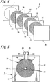
- FIG. 1 is an exploded perspective view of a coil module apparatus according to a first embodiment of the present invention
- FIG. 2 is a perspective view of the coil module apparatus according to the first embodiment after assembly.
- the coil module apparatus according to the present embodiment includes a first case piece 1, a second case piece 2 and a secondary side transfer coil 3.
- the first case piece 1 and second case piece 2 are formed of ABS (Acrylonitrile Butadiene Styrene copolymer) resin or the like and form an internal enclosure when placed facing one another and connected to one another.
- the secondary side transfer coil 3 has a flat shape and charges a battery pack of the mobile phone unit based on transfer power transferred from a primary side transfer coil of a cradle apparatus during contactless charging.
- the coil module apparatus further includes a circuit board 4, a temperature sensor 5, a double-sided tape sheet 6, and a magnetic sheet 7.
- the circuit board 4 carries out charging control during contactless charging, control over the transmission and reception of predetermined data, and the like.
- the temperature sensor 5 detects the temperature of the secondary side transfer coil 3 during contactless charging.
- the double-sided tape sheet 6 is provided so as to cover the secondary side transfer coil 3 from the opposite side to the first case piece 1.
- the magnetic sheet 7 is stuck onto the secondary side transfer coil 3 via the double-sided tape sheet 6 so as to cover the secondary side transfer coil 3.
- the coil module apparatus further includes a double-sided tape sheet 8 and a metal sheet 9.
- the double-sided tape sheet 8 is stuck onto the magnetic sheet 7.
- the metal sheet 9 is stuck onto the secondary side transfer coil 3 via the double-sided tape sheet 8 and the magnetic sheet 7 so as to cover the secondary side transfer coil 3. That is, the magnetic sheet 7 and the metal sheet 9 are stuck in that order on the secondary side transfer coil 3 via the double-sided tape sheet 6 and the double-sided tape sheet 8, respectively.
- Connection terminals 10 are provided on the second case piece 2 and when the coil module apparatus is attached to the mobile phone unit, the connection terminals 10 are connected to connection terminals provided on the mobile phone unit for the electrical continuity of the secondary side transfer coil 3, the circuit board 4, and the temperature sensor 5.
- the first case piece 1 and the second case piece 2 are placed facing one another and connected to one another with the components from the secondary side transfer coil 3 to the metal sheet 9 enclosed therein and by doing so, a rectangular box-shaped coil module apparatus as shown in FIG. 2 is formed.
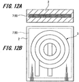
- the secondary side transfer coil 3 is formed by sticking a flat coil, which is produced by winding a wire 20 such as a solid wire or stranded wire with an insulating layer formed on the surface thereof into a spiral on a substantially flat plane, via an adhesive sheet onto a flexible printed circuit board 21.
- the flexible printed circuit board 21 is an extremely thin sheet-like circuit board made of a material such as polyimide resin and has a surface insulating layer formed thereon.
- the surface insulating layer is formed on the surface excluding a first coil connecting portion 23, a second coil connecting portion 25, and a first external connection terminal portion 26, and a second external connection terminal portion 27.
- the first coil connecting portion 23 is located inside an inner periphery portion 22 of the flat coil when the flat coil has been stuck to the flexible printed circuit board 21.
- the second coil connecting portion 25 is located in a periphery outside an outer periphery portion 24 of the flat coil when the flat coil has been stuck to the flexible printed circuit board 21.
- the first coil connecting portion 23 and the first external connection terminal portion 26 are electrically connected via a first internal wiring pattern 28 formed under the surface insulating layer.
- the second coil connecting portion 25 and the second external connection terminal portion 27 are electrically connected via a second internal wiring pattern 29 formed under the surface insulating layer.
- the secondary side transfer coil 3 has no parts where the wire 20 overlaps itself, so that the thickness of the secondary side transfer coil 3 can be made extremely thin.
- the magnetic sheet 7 and the metal sheet 9 are stuck via the double-sided tape sheet 6 and the double-sided tape sheet 8 respectively on the opposite surface of the secondary side transfer coil 3 to the surface on the first case piece 1-side.
- the magnetic sheet 7 and the metal sheet 9 are provided to efficiently form magnetic paths for the secondary side transfer coil 3 to increase the magnetic flux during contactless charging and also suppress unnecessary radiation due to magnetic fields produced during contactless charging.
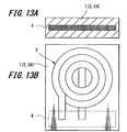
- a flat coil with a multilayer structure formed by stacking a plurality of flexible printed circuit boards on which flat coil patterns made of spiral conductive patterns have been formed may be used as the secondary side transfer coil 3 other than a flat coil formed using the wire 20 as shown in FIG. 3 .
- the secondary side transfer coil 3 includes a four-layer structure.
- a first layer circuit board 31, a second layer circuit board 32, a third layer circuit board 33, and a fourth layer circuit board 34 are respectively formed of wiring conductive patterns 35 that have been wound in spirals on sheet-like circuit boards of a material such as polyimide resin.
- a surface insulating layer 36 is formed on a surface of the first layer circuit board 31 as a topmost layer, and an adhesive layer and an insulating interlayer are formed in between the first layer circuit board 31 and the second layer circuit board 32.
- an adhesive layer and an insulating interlayer are formed in between the second layer circuit board 32 and the third layer circuit board 33 and an adhesive layer and an insulating interlayer are formed in between the third layer circuit board 33 and the fourth layer circuit board 34.
- the magnetic sheet 7 and the metal sheet 9 are stuck onto the rear surface of the fourth layer circuit board 34 that is the bottommost layer via an adhesive layer and an insulating interlayer.
- pattern ends of inner periphery portions 37 of conductive patterns 35 on the first layer circuit board 31 to the fourth layer circuit board 34 are electrically connected via first through-holes 38.
- pattern ends of outer periphery portions 39 of the conductive patterns 35 on the first layer circuit board 31 to the fourth layer circuit board 34 are electrically connected via second through-holes 40.
- first through-holes 38 on the inner periphery portion 37 side of the conductive patterns 35 on each layer are electrically connected to third through-holes 41 provided on the outer periphery portion 39 side of the conductive patterns 35 on each layer.
- the second through-holes 40 of the fourth layer circuit board 34 are electrically connected via a second internal conductive pattern 42 to a second external connecting terminal portion 44.
- the first through-holes 38 of the fourth layer circuit board 34 are electrically connected via the third through-holes 41 and a first internal conductive pattern 43 to a first external connecting terminal portion 45.
- the flat coil is formed by the conductive patterns 35 of the flexible printed circuit boards 31 to 34 on each layer, and therefore the thickness can be made even slimmer than the flat coil that uses the wire 20 described earlier.
- FIG. 6A is a cross-sectional view of a mobile phone unit in which a coil module apparatus 50 is installed.
- the mobile phone unit is a stick-shaped mobile phone unit and includes a battery pack attachment hole portion 52 that encloses a battery pack 51 on a rear surface of an operation unit and a coil module hole portion 53 that encloses the coil module apparatus 50 on a rear surface of a display unit.
- connection terminals 10 provided on the coil module apparatus 50 and connection terminals provided on the mobile phone unit are in contact and electrically connected.
- the battery pack 51 is attached to the battery pack attachment hole portion 52 of the mobile phone unit and then the rear cover 54 is attached.
- the coil module apparatus 50 is attached inside the mobile phone unit.
- the coil module apparatus 50 is attached to the rear surface of the display unit in this example.
- an insertion hole portion for the coil module apparatus 50 may instead be provided on a base surface portion 55 of the mobile terminal shown in FIG. 6A . Accordingly, by inserting the coil module apparatus 50 via this insertion hole portion, the coil module apparatus 50 can be attached between the battery pack 51 and the rear cover 54.
- the insertion hole portion of the coil module apparatus 50 may be provided on a side surface portion of the mobile phone unit and the coil module apparatus 50 may be attached via the insertion hole portion from the side surface portion of the mobile phone unit.
- the first case piece 1 and the second case piece 2 are placed facing one another and connected with the components from the secondary side transfer coil 3 to the metal sheet 9 enclosed therein to assemble a flat coil into a module.
- the resistance to bending and the strength of a flat coil that has been made slim can be obtained with the first case piece 1 and the second case piece 2.
- the coil module apparatus may only need to be inserted inside the mobile phone unit, so that the flat coil is incorporated in a simplified manner. Accordingly, the ease and productivity of the incorporating process can be improved.
- the first case piece 1 and the second case piece 2 are formed so as to enclose the components from the secondary side transfer coil 3 to the metal sheet 9 in the coil module apparatus according to the first embodiment.
- a coil module apparatus according to a second embodiment is formed using a rear cover of a charged appliance, such as a mobile phone unit, as the first case piece 1 described above.
- FIG. 7 is an exploded perspective view of the coil module apparatus according to the second embodiment
- FIG. 8 is a perspective view of the coil module apparatus according to the second embodiment after assembly.
- the coil module apparatus according to the second embodiment is formed so that the components from the secondary side transfer coil 3 to the metal sheet 9 are enclosed by the rear cover 54 of the mobile phone unit shown in FIG. 6A and FIG. 6B and the second case piece 2 described above.
- the coil module apparatus according to the second embodiment uses the rear cover 54 of the mobile phone unit in place of the first case piece 1 described above.
- the coil module apparatus according to the second embodiment is formed so as to enclose components from the secondary side transfer coil 3 to the metal sheet 9 in an enclosure region internally formed by placing the rear cover 54 and the second case piece 2 facing one another.
- FIG. 9A is a cross-sectional view of a mobile phone unit to which a coil module apparatus 60 according to the second embodiment is attached.
- the mobile phone unit is a stick-shaped mobile phone unit, and includes, on a rear surface of an operation unit, a battery pack attachment hole portion 52 that encloses the battery pack 51 and a coil module gap portion 61 that encloses the coil module apparatus 60.
- the coil module apparatus 60 When the coil module apparatus 60 is attached to such a mobile phone unit, after the battery pack 51 has been attached to the battery pack attachment hole portion 52, the coil module apparatus 60 is attached to the mobile phone unit by attaching the rear cover to the mobile phone unit. By doing so, as shown in FIG. 9B , using the rear cover 54 in place of the first case piece 1 in addition to using it as the cover of the mobile phone unit, the coil module apparatus 60 is enclosed inside the coil module gap portion 61, thereby attaching the coil module apparatus to the mobile phone unit.
- the first case piece 1 that forms the coil module apparatus is also used as the rear cover of a charged appliance such as a mobile phone unit, which makes it possible to reduce the number of components, in addition to achieving the same effect as the first embodiment described earlier.
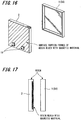
- a groove portion 70 into which the secondary side transfer coil 3 is fitted may be provided on the first case piece 1 or on the rear cover 54 of the mobile phone unit (or charged appliance).
- the groove portion 70 is formed in accordance with the overall form of the secondary side transfer coil 3 formed by the wire 20. This means that by fitting the secondary side transfer coil 3 into the groove portion 70, the secondary side transfer coil 3 can be fixed to the first case piece 1 or the rear cover 54 with the secondary side transfer coil 3 correctly positioned. Also, with the groove portion 70, the positioning on the first case piece 1 or the rear cover 54 can be simplified.
- the secondary side transfer coil 3 may be insert molded inside the first case piece 1 or the rear cover 54 of the mobile phone unit (or charged appliance). By doing so, it is possible to fix the secondary side transfer coil 3 to the first case piece 1 or the rear cover 54 having correctly positioned the secondary side transfer coil 3 and to also prevent short circuits for the secondary side transfer coil 3. In addition, it is possible to omit a structure for positioning the secondary side transfer coil 3 that is provided on the first case piece 1 or the rear cover 54.
- the magnetic sheet 7 and/or the metal sheet 9 may be insert molded inside the second case piece 2.
- the magnetic sheet 7 and the metal sheet 9 become sealed inside the second case piece 2, it is possible to prevent conductive particles from dispersing from the magnetic sheet 7 and the metal sheet 9.
- the circuit board 4 may be insert molded inside the first case piece 1, the second case piece 2, or the rear cover 54. By doing so, it is possible to easily position and dispose the circuit board 4, and since the circuit board 4 becomes sealed inside the first case piece 1, the second case piece 2, or the rear cover 54, it is possible to prevent short circuits for the circuit board 4.
- the temperature sensor 5 may be insert molded inside the first case piece 1, the second case piece 2, or the rear cover 54. By doing so, it is possible to easily position and dispose the temperature sensor 5, and since the temperature sensor 5 becomes sealed inside the first case piece 1, the second case piece 2, or the rear cover 54, it is possible to prevent short circuits for the temperature sensor 5.
- a multilayer circuit board may be used as the circuit board 4.
- the temperature sensor 5 may be provided between any of the layers of the multilayer circuit board, and the multilayer circuit board provided with the temperature sensor 5 may be insert molded inside the first case piece 1, the second case piece 2, or the rear cover 54. By doing so, it is possible to easily position and dispose the circuit board 4 and the temperature sensor 5, and since the circuit board 4 and the temperature sensor 5 become sealed inside the first case piece 1, the second case piece 2, or the rear cover 54, it is possible to prevent short circuits for the circuit board 4 and the temperature sensor 5.
- the entire second case piece 2 or a surface portion of the second case piece 2 that faces the secondary side transfer coil 3 may be formed of a resin in which a magnetic material is mixed.
- the magnetic sheet 7 shown in FIG. 1 or in FIG. 7 can be omitted, and therefore the coil module apparatus can be made even slimmer. Also, since a magnetic material is mixed into the resin, it is possible to prevent conductive particles from dispersing.
- the surface portion of the second case piece 2 that faces the secondary side transfer coil 3 may be formed of a resin in which a magnetic material is mixed and the other surface portion of the second case piece 2 may be formed of normal resin, or in other words, the second case piece 2 may be dual-molded.
- the magnetic sheet 7 shown in FIG. 1 and FIG. 7 it is possible to omit the magnetic sheet 7 shown in FIG. 1 and FIG. 7 , and therefore the coil module apparatus can be made even slimmer.
- the magnetic material is mixed into the resin, it is possible to prevent conductive particles from dispersing.
- the surface portion of the second case piece 2 that faces the secondary side transfer coil 3 may be formed of a resin in which a magnetic material is mixed and the other surface portion thereof may be formed of normal resin.
- the second case piece 2 may be dual-molded.
- the metal sheet 9 may be insert molded inside the second case piece 2.
- the enclosure region of the case pieces 1 and 2 can be made smaller by an amount corresponding to the magnetic sheet 7 and the metal sheet 9, and therefore the coil module apparatus can be made even slimmer.
- a magnetic material is mixed into the resin and the metal sheet 9 is insert molded inside the second case piece 2, it is possible to prevent conductive particles from dispersing.
- the first case piece 1, the second case piece 2, or the rear cover 54 may be dual-molded of a resin in which a magnetic material is mixed and a normal resin, and the secondary side transfer coil 3 may be insert molded between the resin in which the magnetic material is mixed and the normal resin.
- the second case piece 2 may be formed of an elastic resin, i.e., a resin that exhibits elasticity.
- the rear cover 54 (or the first case piece 1) is dual molded of the normal resin and the resin in which the magnetic material is mixed.
- the secondary side transfer coil 3 and the metal sheet 9 are insert molded, and the second case piece 2 formed of the elastic resin is connected to the rear cover 54.
- the battery pack 51 will expand somewhat due to repeated charging.
- the second case piece 2 that contacts the battery pack 51 being formed of elastic resin, it will be possible to absorb the expansion of the battery pack 51.
- the present invention has been applied to a coil module apparatus of a mobile phone unit in the embodiments described above, the present invention can be applied to a coil module apparatus for a PHS (Personal Handyphone System) telephone, a PDA (Personal Digital Assistant), a mobile game device, a digital camera apparatus, or a notebook computer. By doing so, the same effects as described above can be obtained.
- a PHS Personal Handyphone System
- PDA Personal Digital Assistant
Landscapes
- Engineering & Computer Science (AREA)
- Power Engineering (AREA)
- Telephone Set Structure (AREA)
- Coils Or Transformers For Communication (AREA)
Claims (15)
- Spulenmodul-Vorrichtung, umfassend:eine Flachspule (3) mit einer flachen Form;eine Schaltplatine (4) für die Flachspule (3);eine Magnetplatte (7), die bereitgestellt wird, um einen Oberflächenabschnitt der Flachspule (3) zu bedecken;Anschlussklemmen (10) zum Anschließen der Flachspule (3) und der Schaltplatine (4);ein Gehäuse (1, 2), welches die Flachspule (3), die Schaltplatine (4) und die Magnetplatte (7) umschließt und die Anschlussklemmen (10) so umschließt, dass die Anschlussklemmen (10) teilweise freiliegen; undeine Metallplatte (9), die innerhalb des Gehäuses umschlossen ist und so bereitgestellt ist, dass sie die Flachspule (3) von oberhalb der Magnetplatte (7) bedeckt, so dass sich die Magnetplatte (7) zwischen der Metallplatte (9) und der Flachspule (3) befindet; und wobei die Flachspule, die durch Wickeln eines Drahtes, der aus einem von einem leitenden Einzeldraht und einem leitenden verdrillten Draht besteht, zu einer Spirale auf einer im Wesentlichen flachen Ebene gebildet ist, innerhalb eines Oberflächenabschnitts des Gehäuses durch Inserttechnik geformt ist.
- Spulenmodul-Vorrichtung nach Anspruch 1, wobei die Flachspule eine der folgenden ist:eine Flachspule, die durch Wickeln eines Drahtes, der aus einem von einem leitenden Einzeldraht und einem leitenden verdrillten Draht besteht, zu einer Spirale auf einer im Wesentlichen flachen Ebene gebildet ist, undeine Flachspule, die durch Stapeln einer Vielzahl von leitenden Strukturschaltplatinen gebildet ist, auf denen leitende Strukturen, die jeweils Teil der Flachspule bilden, gebildet sind, so dass aus den leitenden Strukturen eine spiralige Flachspulenstruktur gebildet wird, und die leitenden Strukturen elektrisch verbunden werden.
- Flachspulen-Vorrichtung nach Anspruch 1, wobei die in dem Gehäuse umschlossene Flachspule eine Flachspule ist, die durch Wickeln eines Drahtes, der aus einem von einem leitenden Einzeldraht und einem leitenden verdrillten Draht besteht, zu einer Spirale auf einer im Wesentlichen flachen Ebene gebildet ist, und das Gehäuse einen Flachspuleninsertabschnitt in Form einer Nut mit einer Gestalt einschließt, die der Flachspule entspricht, und in einem Oberflächenabschnitt bereitgestellt wird, der in Kontakt mit der Flachspule ist.
- Spulenmodul-Vorrichtung nach Anspruch 1, wobei die Magnetplatte innerhalb des Gehäuses durch Inserttechnik geformt ist.
- Spulenmodul-Vorrichtung nach Anspruch 1, wobei die Magnetplatte integral mit einem Oberflächenabschnitt des Gehäuses gebildet ist, indem ein magnetisches Material in ein vorbestimmtes Harz gemischt wird, das den einen Oberflächenabschnitt des Gehäuses bildet.
- Spulenmodul-Vorrichtung nach Anspruch 1, wobei die Magnetplatte durch Mischen eines magnetischen Materials in ein vorbestimmtes Harz gebildet wird, und ein Oberflächenabschnitt des Gehäuses aus einem Harz, das die eine Oberfläche des Gehäuses bildet, und der Magnetplatte, die durch Mischen des magnetischen Materials in das vorbestimmte Harz gebildet wird, doppelgeformt wird.
- Spulenmodul-Vorrichtung nach Anspruch 6, wobei die Flachspule zwischen dem Harz, das den einen Oberflächenabschnitt des Gehäuses bildet, und der Magnetplatte, die durch Mischen des magnetischen Materials in das vorbestimmte Harz gebildet ist, durch Inserttechnik geformt ist.
- Spulenmodul-Vorrichtung nach Anspruch 1, wobei die Metallplatte innerhalb des Gehäuses durch Inserttechnik geformt ist.
- Spulenmodul-Vorrichtung nach Anspruch 8, wobei die Metallplatte zwischen dem Harz, das einen Oberflächenabschnitt des Gehäuses bildet, und der Magnetplatte, die durch Mischen des magnetischen Materials in das vorbestimmte Harz gebildet ist, durch Inserttechnik geformt ist.
- Spulenmodul-Vorrichtung nach Anspruch 1, ferner umfassend eine Temperaturdetektiereinheit, die innerhalb des Gehäuses umschlossen ist und eine Temperatur der Flachspule detektiert.
- Spulenmodul-Vorrichtung nach Anspruch 10, wobei die Temperaturdetektiereinheit innerhalb eines Oberflächenabschnitts des Gehäuses durch Inserttechnik geformt ist.
- Spulenmodul-Vorrichtung nach Anspruch 1, wobei die Schaltplatine innerhalb eines Oberflächenabschnitts des Gehäuses durch Inserttechnik geformt ist.
- Spulenmodul-Vorrichtung nach Anspruch 12, wobei die in dem Gehäuse durch Inserttechnik geformte Schaltplatine aus einer mehrschichtigen Schaltplatine besteht, und die Temperaturdetektiereinheit zwischen jedweden zwei Schichten der mehrschichtigen Schaltplatine bereitgestellt wird.
- Spulenmodul-Vorrichtung nach Anspruch 1, wobei ein Oberflächenabschnitt des Gehäuses, welches in Gebrauch in Kontakt mit einem Batteriepack ist, aus elastischem Harz gebildet ist.
- Spulenmodul-Vorrichtung nach Anspruch 1, wobei ein Oberflächenabschnitt des Gehäuses, der zu einem Oberflächenabschnitt der Flachspule weist, der dem Oberflächenabschnitt gegenüber liegt, der durch die Magnetplatte bedeckt ist, verarbeitet wird, damit er als hintere Abdeckung eines geladenen Gerät gestaltet ist, an dem die Spulenmodul-Vorrichtung befestigt wird.
Applications Claiming Priority (1)
| Application Number | Priority Date | Filing Date | Title |
|---|---|---|---|
| JP2007141690A JP4896820B2 (ja) | 2007-05-29 | 2007-05-29 | コイルモジュール装置 |
Publications (3)
| Publication Number | Publication Date |
|---|---|
| EP1998342A2 EP1998342A2 (de) | 2008-12-03 |
| EP1998342A3 EP1998342A3 (de) | 2014-07-09 |
| EP1998342B1 true EP1998342B1 (de) | 2018-01-10 |
Family
ID=39712160
Family Applications (1)
| Application Number | Title | Priority Date | Filing Date |
|---|---|---|---|
| EP08251854.9A Active EP1998342B1 (de) | 2007-05-29 | 2008-05-28 | Spulenmodul-Vorrichtung |
Country Status (4)
| Country | Link |
|---|---|
| US (1) | US7852184B2 (de) |
| EP (1) | EP1998342B1 (de) |
| JP (1) | JP4896820B2 (de) |
| CN (1) | CN101383215A (de) |
Families Citing this family (41)
| Publication number | Priority date | Publication date | Assignee | Title |
|---|---|---|---|---|
| JP5659504B2 (ja) * | 2010-03-02 | 2015-01-28 | 富士通株式会社 | 電磁波特性改善用シート体 |
| KR101134625B1 (ko) * | 2010-07-16 | 2012-04-09 | 주식회사 한림포스텍 | 무선 전력 통신용 코어 어셈블리와 그를 구비하는 무선 전력 통신용 전력 공급 장치, 그리고 무선 전력 통신용 코어 어셈블리 제조 방법 |
| JP5532422B2 (ja) * | 2010-07-30 | 2014-06-25 | スミダコーポレーション株式会社 | コイル |
| EP2667390B1 (de) | 2011-01-19 | 2018-10-31 | Technova Inc. | System für kontaktfreie energieübertragung |
| US20130293191A1 (en) | 2011-01-26 | 2013-11-07 | Panasonic Corporation | Non-contact charging module and non-contact charging instrument |
| JP2012178531A (ja) * | 2011-02-28 | 2012-09-13 | Equos Research Co Ltd | アンテナ |
| JP2012178529A (ja) * | 2011-02-28 | 2012-09-13 | Equos Research Co Ltd | アンテナ |
| JP5703842B2 (ja) * | 2011-02-28 | 2015-04-22 | 三菱マテリアル株式会社 | 温度センサ付き非接触給電装置 |
| JP2012178530A (ja) * | 2011-02-28 | 2012-09-13 | Equos Research Co Ltd | アンテナ |
| WO2012172812A1 (ja) | 2011-06-14 | 2012-12-20 | パナソニック株式会社 | 通信装置 |
| JP5457478B2 (ja) * | 2011-06-14 | 2014-04-02 | パナソニック株式会社 | 携帯端末 |
| JP2013038893A (ja) * | 2011-08-08 | 2013-02-21 | Equos Research Co Ltd | 電力伝送システム |
| US10204734B2 (en) | 2011-11-02 | 2019-02-12 | Panasonic Corporation | Electronic device including non-contact charging module and near field communication antenna |
| JP5965148B2 (ja) * | 2012-01-05 | 2016-08-03 | 日東電工株式会社 | 無線電力伝送を用いたモバイル端末用受電モジュール及び当該モバイル端末用受電モジュールを備えたモバイル端末用充電池 |
| US8760253B2 (en) * | 2012-01-17 | 2014-06-24 | Delphi Technologies, Inc. | Electrical coil assembly including a ferrite layer and a thermally-conductive silicone layer |
| JP2013169122A (ja) | 2012-02-17 | 2013-08-29 | Panasonic Corp | 非接触充電モジュール及びそれを備えた携帯端末 |
| JP6112383B2 (ja) | 2012-06-28 | 2017-04-12 | パナソニックIpマネジメント株式会社 | 携帯端末 |
| US9179558B1 (en) | 2012-09-17 | 2015-11-03 | Brite Case, LLC | Case with panel for display |
| JP6034644B2 (ja) * | 2012-10-10 | 2016-11-30 | デクセリアルズ株式会社 | 複合コイルモジュール、及び携帯機器 |
| KR101963261B1 (ko) | 2013-03-22 | 2019-03-28 | 삼성전기주식회사 | 무선 충전 장치 |
| DE102013210411A1 (de) * | 2013-06-05 | 2014-12-11 | Robert Bosch Gmbh | Spulenvorrichtung und Verfahren zur induktiven Leistungsübertragung |
| US9837204B2 (en) * | 2013-12-17 | 2017-12-05 | Qualcomm Incorporated | Coil topologies for inductive power transfer |
| JP2015142019A (ja) * | 2014-01-29 | 2015-08-03 | トヨタ自動車株式会社 | 受電装置 |
| KR101762778B1 (ko) | 2014-03-04 | 2017-07-28 | 엘지이노텍 주식회사 | 무선 충전 및 통신 기판 그리고 무선 충전 및 통신 장치 |
| US10329019B2 (en) | 2014-04-07 | 2019-06-25 | Safran Seats Usa Llc | Inductive power transmission in aircraft seats |
| US9621016B2 (en) * | 2014-08-20 | 2017-04-11 | Apple Inc. | Flat coil assembly for Lorentz actuator mechanism |
| EP2992776B1 (de) * | 2014-09-04 | 2019-11-06 | WITS Co., Ltd. | Gehäuse und vorrichtung damit |
| US10643787B2 (en) * | 2015-02-11 | 2020-05-05 | Fu Da Tong Technology Co., Ltd. | Induction type power supply system and coil module thereof |
| KR102484849B1 (ko) * | 2015-12-18 | 2023-01-05 | 주식회사 위츠 | 코일 조립체 |
| JP6717127B2 (ja) | 2016-09-02 | 2020-07-01 | 株式会社Ihi | コイル装置、保持部材および保持部材セット |
| USD812556S1 (en) * | 2016-12-02 | 2018-03-13 | Guangdong Bestek E-Commerce Co., Ltd. | Wireless charger |
| CN106451810A (zh) * | 2016-12-05 | 2017-02-22 | 青岛鲁渝能源科技有限公司 | 防漏电保护器和手机充电系统 |
| KR102703563B1 (ko) * | 2017-02-01 | 2024-09-06 | 삼성전자주식회사 | 디스플레이 시스템, 무선 전력 송신 장치 및 무선 전력 수신 장치 |
| US10638031B1 (en) | 2017-03-29 | 2020-04-28 | Apple Inc. | Additive coil structure for voice coil motor actuator |
| EP3825668B1 (de) * | 2017-04-11 | 2022-11-02 | Shibaura Electronics Co., Ltd. | Temperatursensor |
| CN107068369A (zh) * | 2017-06-01 | 2017-08-18 | 班戈设备系统(苏州)有限公司 | 一种防辐射变压器 |
| EP3786988A4 (de) * | 2018-06-11 | 2021-09-01 | Guangdong Oppo Mobile Telecommunications Corp., Ltd. | Drahtlose ladespule, drahtlose ladeanordnung und elektronische vorrichtung |
| KR20210075550A (ko) * | 2019-12-13 | 2021-06-23 | 삼성전자주식회사 | 코일들을 포함하는 전자 장치 |
| PL73205Y1 (pl) * | 2021-07-15 | 2023-12-04 | Siec Badawcza Lukasiewicz Inst Metali Niezelaznych | Przekładka, zwłaszcza do dławików magnetycznych |
| CN114190022B (zh) * | 2021-10-28 | 2022-11-04 | 荣耀终端有限公司 | 电子设备 |
| CN117278077A (zh) * | 2022-06-14 | 2023-12-22 | 台湾东电化股份有限公司 | 无线传输模块 |
Family Cites Families (18)
| Publication number | Priority date | Publication date | Assignee | Title |
|---|---|---|---|---|
| JPS6149423A (ja) * | 1984-08-17 | 1986-03-11 | Matsushita Electronics Corp | 半導体装置の製造方法 |
| US5375040A (en) * | 1992-09-29 | 1994-12-20 | Eldec Corporation | Modular electronic circuit housing and wiring board |
| JPH07264779A (ja) * | 1994-03-18 | 1995-10-13 | Sony Corp | 電磁誘導充電システム |
| JPH08148359A (ja) * | 1994-11-18 | 1996-06-07 | Tdk Corp | Lan用コネクタ |
| JP3430807B2 (ja) * | 1996-07-25 | 2003-07-28 | 松下電工株式会社 | 充電式電気機器 |
| JP3697789B2 (ja) * | 1996-09-20 | 2005-09-21 | 松下電器産業株式会社 | 非接触型電源装置 |
| US5835350A (en) * | 1996-12-23 | 1998-11-10 | Lucent Technologies Inc. | Encapsulated, board-mountable power supply and method of manufacture therefor |
| JP3818478B2 (ja) * | 1998-09-08 | 2006-09-06 | シャープ株式会社 | シート型トランス、その製造方法およびシート型トランスを含むスイッチング電源モジュール |
| JP2000269059A (ja) * | 1999-03-16 | 2000-09-29 | Nippon Telegr & Teleph Corp <Ntt> | 磁性部品およびその製造方法 |
| JP3652936B2 (ja) * | 1999-10-12 | 2005-05-25 | 株式会社豊田自動織機 | 充電用給電パドル及び充電用給電パドルの製造方法 |
| JP2002175922A (ja) * | 2000-12-08 | 2002-06-21 | Sansha Electric Mfg Co Ltd | 高周波大電流変圧器 |
| EP1547222B1 (de) * | 2002-06-10 | 2018-10-03 | City University of Hong Kong | Planares induktives batterieladegerät |
| JP2005269599A (ja) * | 2004-02-18 | 2005-09-29 | Sony Corp | アンテナモジュール用磁芯部材およびその製造方法 |
| JP2005260122A (ja) * | 2004-03-15 | 2005-09-22 | Dainippon Printing Co Ltd | 非接触電力伝送モジュール |
| JP2006339757A (ja) * | 2005-05-31 | 2006-12-14 | Denso Corp | アンテナコイル、通信基板モジュールの製造方法及びカード型無線機 |
| JP2006339329A (ja) | 2005-06-01 | 2006-12-14 | Seiko Epson Corp | 平面コイル装置及び基板並びに平面コイル固定方法 |
| US7495414B2 (en) * | 2005-07-25 | 2009-02-24 | Convenient Power Limited | Rechargeable battery circuit and structure for compatibility with a planar inductive charging platform |
| KR101122983B1 (ko) * | 2007-02-20 | 2012-03-15 | 세이코 엡슨 가부시키가이샤 | 코일 유닛 및 전자 기기 |
-
2007
- 2007-05-29 JP JP2007141690A patent/JP4896820B2/ja active Active
-
2008
- 2008-05-28 US US12/153,935 patent/US7852184B2/en active Active
- 2008-05-28 EP EP08251854.9A patent/EP1998342B1/de active Active
- 2008-05-29 CN CNA2008101428514A patent/CN101383215A/zh active Pending
Non-Patent Citations (1)
| Title |
|---|
| None * |
Also Published As
| Publication number | Publication date |
|---|---|
| EP1998342A3 (de) | 2014-07-09 |
| JP2008300398A (ja) | 2008-12-11 |
| US7852184B2 (en) | 2010-12-14 |
| CN101383215A (zh) | 2009-03-11 |
| EP1998342A2 (de) | 2008-12-03 |
| US20080297295A1 (en) | 2008-12-04 |
| JP4896820B2 (ja) | 2012-03-14 |
Similar Documents
| Publication | Publication Date | Title |
|---|---|---|
| EP1998342B1 (de) | Spulenmodul-Vorrichtung | |
| US8169286B2 (en) | Coil unit, method of manufacturing the same, and electronic instrument | |
| US8771852B2 (en) | Battery pack with contactless power transfer | |
| CN102037714A (zh) | 便携式通信终端的集成天线和emi屏蔽支撑构件 | |
| CN101420076A (zh) | 连接器组件 | |
| US20140050945A1 (en) | Intrinsically safe battery pack | |
| CN213124646U (zh) | 电子设备 | |
| JP3952434B2 (ja) | 電池パックおよびその製造方法 | |
| CN112187970A (zh) | 摄像头模组及其电子装置 | |
| JP3686785B2 (ja) | 信号ケーブル | |
| US9439286B2 (en) | Connecting device for electronic component of electronic device | |
| CN108701929A (zh) | 导向器组合式接触器及包括其的便携式电子装置 | |
| US20240405472A1 (en) | Durable reduced-size power adapters | |
| JP2004185861A (ja) | 回路基板及び電池パック | |
| US12255387B2 (en) | Mobile electronic device | |
| KR101092315B1 (ko) | 측면 안테나를 구비한 배터리팩 | |
| CN211720831U (zh) | 一种电子设备 | |
| CN221551971U (zh) | 一种电芯保护板、电池及电子设备 | |
| CN221552028U (zh) | 一种电池组件及电子设备 | |
| KR100761423B1 (ko) | 선형 패턴의 그라운드층을 구비하는 연성회로기판 | |
| KR101429766B1 (ko) | 전지 팩 | |
| KR20170142651A (ko) | 안테나 모듈 및 이를 구비하는 이동 단말기 | |
| TWI345341B (en) | Connector assembly | |
| CN118301841A (zh) | 柔性印刷电路上的作为加强件的屏蔽罩 | |
| JP2009158808A (ja) | フレキシブル基板及びこれを用いた携帯電子機器 |
Legal Events
| Date | Code | Title | Description |
|---|---|---|---|
| PUAI | Public reference made under article 153(3) epc to a published international application that has entered the european phase |
Free format text: ORIGINAL CODE: 0009012 |
|
| AK | Designated contracting states |
Kind code of ref document: A2 Designated state(s): AT BE BG CH CY CZ DE DK EE ES FI FR GB GR HR HU IE IS IT LI LT LU LV MC MT NL NO PL PT RO SE SI SK TR |
|
| AX | Request for extension of the european patent |
Extension state: AL BA MK RS |
|
| RAP1 | Party data changed (applicant data changed or rights of an application transferred) |
Owner name: SONY MOBILE COMMUNICATIONS JAPAN, INC. Owner name: SEIKO EPSON CORPORATION |
|
| PUAL | Search report despatched |
Free format text: ORIGINAL CODE: 0009013 |
|
| AK | Designated contracting states |
Kind code of ref document: A3 Designated state(s): AT BE BG CH CY CZ DE DK EE ES FI FR GB GR HR HU IE IS IT LI LT LU LV MC MT NL NO PL PT RO SE SI SK TR |
|
| AX | Request for extension of the european patent |
Extension state: AL BA MK RS |
|
| RIC1 | Information provided on ipc code assigned before grant |
Ipc: H01F 27/28 20060101ALI20140605BHEP Ipc: H01F 27/36 20060101ALI20140605BHEP Ipc: H01F 27/04 20060101AFI20140605BHEP Ipc: H01F 27/02 20060101ALI20140605BHEP Ipc: H01F 5/00 20060101ALI20140605BHEP Ipc: H01F 27/29 20060101ALI20140605BHEP Ipc: H01F 38/14 20060101ALI20140605BHEP |
|
| 17P | Request for examination filed |
Effective date: 20150109 |
|
| RBV | Designated contracting states (corrected) |
Designated state(s): AT BE BG CH CY CZ DE DK EE ES FI FR GB GR HR HU IE IS IT LI LT LU LV MC MT NL NO PL PT RO SE SI SK TR |
|
| AKX | Designation fees paid |
Designated state(s): DE FR GB |
|
| AXX | Extension fees paid |
Extension state: BA Extension state: RS Extension state: AL Extension state: MK |
|
| STAA | Information on the status of an ep patent application or granted ep patent |
Free format text: STATUS: EXAMINATION IS IN PROGRESS |
|
| 17Q | First examination report despatched |
Effective date: 20170222 |
|
| GRAP | Despatch of communication of intention to grant a patent |
Free format text: ORIGINAL CODE: EPIDOSNIGR1 |
|
| STAA | Information on the status of an ep patent application or granted ep patent |
Free format text: STATUS: GRANT OF PATENT IS INTENDED |
|
| INTG | Intention to grant announced |
Effective date: 20170731 |
|
| RIN1 | Information on inventor provided before grant (corrected) |
Inventor name: SUZUKI, KATSUYA Inventor name: JIN, MIKIMOTO Inventor name: SUZUKI, KUNIHARU Inventor name: YODA, KENTARO Inventor name: ONISHI, KOTA Inventor name: KONDO, YOICHIRO Inventor name: YAMAZAKI, MANABU Inventor name: KATO, HIROSHI |
|
| RAP1 | Party data changed (applicant data changed or rights of an application transferred) |
Owner name: SEIKO EPSON CORPORATION Owner name: SONY MOBILE COMMUNICATIONS INC. |
|
| GRAS | Grant fee paid |
Free format text: ORIGINAL CODE: EPIDOSNIGR3 |
|
| GRAA | (expected) grant |
Free format text: ORIGINAL CODE: 0009210 |
|
| STAA | Information on the status of an ep patent application or granted ep patent |
Free format text: STATUS: THE PATENT HAS BEEN GRANTED |
|
| AK | Designated contracting states |
Kind code of ref document: B1 Designated state(s): DE FR GB |
|
| REG | Reference to a national code |
Ref country code: GB Ref legal event code: FG4D |
|
| REG | Reference to a national code |
Ref country code: DE Ref legal event code: R096 Ref document number: 602008053731 Country of ref document: DE |
|
| REG | Reference to a national code |
Ref country code: DE Ref legal event code: R097 Ref document number: 602008053731 Country of ref document: DE |
|
| PLBE | No opposition filed within time limit |
Free format text: ORIGINAL CODE: 0009261 |
|
| STAA | Information on the status of an ep patent application or granted ep patent |
Free format text: STATUS: NO OPPOSITION FILED WITHIN TIME LIMIT |
|
| 26N | No opposition filed |
Effective date: 20181011 |
|
| GBPC | Gb: european patent ceased through non-payment of renewal fee |
Effective date: 20180528 |
|
| PG25 | Lapsed in a contracting state [announced via postgrant information from national office to epo] |
Ref country code: GB Free format text: LAPSE BECAUSE OF NON-PAYMENT OF DUE FEES Effective date: 20180528 Ref country code: FR Free format text: LAPSE BECAUSE OF NON-PAYMENT OF DUE FEES Effective date: 20180531 |
|
| REG | Reference to a national code |
Ref country code: DE Ref legal event code: R082 Ref document number: 602008053731 Country of ref document: DE Representative=s name: DENNEMEYER & ASSOCIATES S.A., DE Ref country code: DE Ref legal event code: R081 Ref document number: 602008053731 Country of ref document: DE Owner name: SEIKO EPSON CORPORATION, JP Free format text: FORMER OWNERS: SEIKO EPSON CORPORATION, TOKYO, JP; SONY MOBILE COMMUNICATIONS INC., TOKYO, JP Ref country code: DE Ref legal event code: R082 Ref document number: 602008053731 Country of ref document: DE Representative=s name: DENNEMEYER & ASSOCIATES RECHTSANWALTSGESELLSCH, DE |
|
| REG | Reference to a national code |
Ref country code: DE Ref legal event code: R082 Ref document number: 602008053731 Country of ref document: DE Representative=s name: DENNEMEYER & ASSOCIATES RECHTSANWALTSGESELLSCH, DE |
|
| PGFP | Annual fee paid to national office [announced via postgrant information from national office to epo] |
Ref country code: DE Payment date: 20250521 Year of fee payment: 18 |