EP1993333A2 - Procédé de fabrication de carte flexible de circuit à étiquette intégrée et structure correspondante - Google Patents
Procédé de fabrication de carte flexible de circuit à étiquette intégrée et structure correspondante Download PDFInfo
- Publication number
- EP1993333A2 EP1993333A2 EP08002193A EP08002193A EP1993333A2 EP 1993333 A2 EP1993333 A2 EP 1993333A2 EP 08002193 A EP08002193 A EP 08002193A EP 08002193 A EP08002193 A EP 08002193A EP 1993333 A2 EP1993333 A2 EP 1993333A2
- Authority
- EP
- European Patent Office
- Prior art keywords
- flexible board
- integrated circuit
- copper foil
- base material
- circuit flexible
- Prior art date
- Legal status (The legal status is an assumption and is not a legal conclusion. Google has not performed a legal analysis and makes no representation as to the accuracy of the status listed.)
- Withdrawn
Links
Images


Classifications
-
- H—ELECTRICITY
- H05—ELECTRIC TECHNIQUES NOT OTHERWISE PROVIDED FOR
- H05K—PRINTED CIRCUITS; CASINGS OR CONSTRUCTIONAL DETAILS OF ELECTRIC APPARATUS; MANUFACTURE OF ASSEMBLAGES OF ELECTRICAL COMPONENTS
- H05K3/00—Apparatus or processes for manufacturing printed circuits
- H05K3/0097—Processing two or more printed circuits simultaneously, e.g. made from a common substrate, or temporarily stacked circuit boards
-
- H—ELECTRICITY
- H05—ELECTRIC TECHNIQUES NOT OTHERWISE PROVIDED FOR
- H05K—PRINTED CIRCUITS; CASINGS OR CONSTRUCTIONAL DETAILS OF ELECTRIC APPARATUS; MANUFACTURE OF ASSEMBLAGES OF ELECTRICAL COMPONENTS
- H05K3/00—Apparatus or processes for manufacturing printed circuits
- H05K3/30—Assembling printed circuits with electric components, e.g. with resistor
- H05K3/32—Assembling printed circuits with electric components, e.g. with resistor electrically connecting electric components or wires to printed circuits
- H05K3/34—Assembling printed circuits with electric components, e.g. with resistor electrically connecting electric components or wires to printed circuits by soldering
-
- H—ELECTRICITY
- H05—ELECTRIC TECHNIQUES NOT OTHERWISE PROVIDED FOR
- H05K—PRINTED CIRCUITS; CASINGS OR CONSTRUCTIONAL DETAILS OF ELECTRIC APPARATUS; MANUFACTURE OF ASSEMBLAGES OF ELECTRICAL COMPONENTS
- H05K3/00—Apparatus or processes for manufacturing printed circuits
- H05K3/007—Manufacture or processing of a substrate for a printed circuit board supported by a temporary or sacrificial carrier
-
- H—ELECTRICITY
- H05—ELECTRIC TECHNIQUES NOT OTHERWISE PROVIDED FOR
- H05K—PRINTED CIRCUITS; CASINGS OR CONSTRUCTIONAL DETAILS OF ELECTRIC APPARATUS; MANUFACTURE OF ASSEMBLAGES OF ELECTRICAL COMPONENTS
- H05K1/00—Printed circuits
- H05K1/18—Printed circuits structurally associated with non-printed electric components
- H05K1/189—Printed circuits structurally associated with non-printed electric components characterised by the use of a flexible or folded printed circuit
-
- H—ELECTRICITY
- H05—ELECTRIC TECHNIQUES NOT OTHERWISE PROVIDED FOR
- H05K—PRINTED CIRCUITS; CASINGS OR CONSTRUCTIONAL DETAILS OF ELECTRIC APPARATUS; MANUFACTURE OF ASSEMBLAGES OF ELECTRICAL COMPONENTS
- H05K2201/00—Indexing scheme relating to printed circuits covered by H05K1/00
- H05K2201/10—Details of components or other objects attached to or integrated in a printed circuit board
- H05K2201/10007—Types of components
- H05K2201/10106—Light emitting diode [LED]
-
- H—ELECTRICITY
- H05—ELECTRIC TECHNIQUES NOT OTHERWISE PROVIDED FOR
- H05K—PRINTED CIRCUITS; CASINGS OR CONSTRUCTIONAL DETAILS OF ELECTRIC APPARATUS; MANUFACTURE OF ASSEMBLAGES OF ELECTRICAL COMPONENTS
- H05K2201/00—Indexing scheme relating to printed circuits covered by H05K1/00
- H05K2201/10—Details of components or other objects attached to or integrated in a printed circuit board
- H05K2201/10613—Details of electrical connections of non-printed components, e.g. special leads
- H05K2201/10621—Components characterised by their electrical contacts
- H05K2201/10674—Flip chip
-
- H—ELECTRICITY
- H05—ELECTRIC TECHNIQUES NOT OTHERWISE PROVIDED FOR
- H05K—PRINTED CIRCUITS; CASINGS OR CONSTRUCTIONAL DETAILS OF ELECTRIC APPARATUS; MANUFACTURE OF ASSEMBLAGES OF ELECTRICAL COMPONENTS
- H05K2201/00—Indexing scheme relating to printed circuits covered by H05K1/00
- H05K2201/20—Details of printed circuits not provided for in H05K2201/01 - H05K2201/10
- H05K2201/2054—Light-reflecting surface, e.g. conductors, substrates, coatings, dielectrics
-
- H—ELECTRICITY
- H05—ELECTRIC TECHNIQUES NOT OTHERWISE PROVIDED FOR
- H05K—PRINTED CIRCUITS; CASINGS OR CONSTRUCTIONAL DETAILS OF ELECTRIC APPARATUS; MANUFACTURE OF ASSEMBLAGES OF ELECTRICAL COMPONENTS
- H05K2203/00—Indexing scheme relating to apparatus or processes for manufacturing printed circuits covered by H05K3/00
- H05K2203/01—Tools for processing; Objects used during processing
- H05K2203/0147—Carriers and holders
- H05K2203/0152—Temporary metallic carrier, e.g. for transferring material
-
- H—ELECTRICITY
- H05—ELECTRIC TECHNIQUES NOT OTHERWISE PROVIDED FOR
- H05K—PRINTED CIRCUITS; CASINGS OR CONSTRUCTIONAL DETAILS OF ELECTRIC APPARATUS; MANUFACTURE OF ASSEMBLAGES OF ELECTRICAL COMPONENTS
- H05K2203/00—Indexing scheme relating to apparatus or processes for manufacturing printed circuits covered by H05K3/00
- H05K2203/01—Tools for processing; Objects used during processing
- H05K2203/0147—Carriers and holders
- H05K2203/0156—Temporary polymeric carrier or foil, e.g. for processing or transferring
-
- H—ELECTRICITY
- H05—ELECTRIC TECHNIQUES NOT OTHERWISE PROVIDED FOR
- H05K—PRINTED CIRCUITS; CASINGS OR CONSTRUCTIONAL DETAILS OF ELECTRIC APPARATUS; MANUFACTURE OF ASSEMBLAGES OF ELECTRICAL COMPONENTS
- H05K2203/00—Indexing scheme relating to apparatus or processes for manufacturing printed circuits covered by H05K3/00
- H05K2203/02—Details related to mechanical or acoustic processing, e.g. drilling, punching, cutting, using ultrasound
- H05K2203/0264—Peeling insulating layer, e.g. foil, or separating mask
-
- H—ELECTRICITY
- H05—ELECTRIC TECHNIQUES NOT OTHERWISE PROVIDED FOR
- H05K—PRINTED CIRCUITS; CASINGS OR CONSTRUCTIONAL DETAILS OF ELECTRIC APPARATUS; MANUFACTURE OF ASSEMBLAGES OF ELECTRICAL COMPONENTS
- H05K2203/00—Indexing scheme relating to apparatus or processes for manufacturing printed circuits covered by H05K3/00
- H05K2203/15—Position of the PCB during processing
- H05K2203/1545—Continuous processing, i.e. involving rolls moving a band-like or solid carrier along a continuous production path
-
- H—ELECTRICITY
- H05—ELECTRIC TECHNIQUES NOT OTHERWISE PROVIDED FOR
- H05K—PRINTED CIRCUITS; CASINGS OR CONSTRUCTIONAL DETAILS OF ELECTRIC APPARATUS; MANUFACTURE OF ASSEMBLAGES OF ELECTRICAL COMPONENTS
- H05K3/00—Apparatus or processes for manufacturing printed circuits
- H05K3/0011—Working of insulating substrates or insulating layers
- H05K3/0044—Mechanical working of the substrate, e.g. drilling or punching
- H05K3/0052—Depaneling, i.e. dividing a panel into circuit boards; Working of the edges of circuit boards
-
- H—ELECTRICITY
- H05—ELECTRIC TECHNIQUES NOT OTHERWISE PROVIDED FOR
- H05K—PRINTED CIRCUITS; CASINGS OR CONSTRUCTIONAL DETAILS OF ELECTRIC APPARATUS; MANUFACTURE OF ASSEMBLAGES OF ELECTRICAL COMPONENTS
- H05K3/00—Apparatus or processes for manufacturing printed circuits
- H05K3/02—Apparatus or processes for manufacturing printed circuits in which the conductive material is applied to the surface of the insulating support and is thereafter removed from such areas of the surface which are not intended for current conducting or shielding
- H05K3/06—Apparatus or processes for manufacturing printed circuits in which the conductive material is applied to the surface of the insulating support and is thereafter removed from such areas of the surface which are not intended for current conducting or shielding the conductive material being removed chemically or electrolytically, e.g. by photo-etch process
- H05K3/061—Etching masks
- H05K3/064—Photoresists
-
- H—ELECTRICITY
- H05—ELECTRIC TECHNIQUES NOT OTHERWISE PROVIDED FOR
- H05K—PRINTED CIRCUITS; CASINGS OR CONSTRUCTIONAL DETAILS OF ELECTRIC APPARATUS; MANUFACTURE OF ASSEMBLAGES OF ELECTRICAL COMPONENTS
- H05K3/00—Apparatus or processes for manufacturing printed circuits
- H05K3/22—Secondary treatment of printed circuits
- H05K3/24—Reinforcing the conductive pattern
- H05K3/244—Finish plating of conductors, especially of copper conductors, e.g. for pads or lands
-
- H—ELECTRICITY
- H05—ELECTRIC TECHNIQUES NOT OTHERWISE PROVIDED FOR
- H05K—PRINTED CIRCUITS; CASINGS OR CONSTRUCTIONAL DETAILS OF ELECTRIC APPARATUS; MANUFACTURE OF ASSEMBLAGES OF ELECTRICAL COMPONENTS
- H05K3/00—Apparatus or processes for manufacturing printed circuits
- H05K3/22—Secondary treatment of printed circuits
- H05K3/28—Applying non-metallic protective coatings
- H05K3/284—Applying non-metallic protective coatings for encapsulating mounted components
-
- H—ELECTRICITY
- H05—ELECTRIC TECHNIQUES NOT OTHERWISE PROVIDED FOR
- H05K—PRINTED CIRCUITS; CASINGS OR CONSTRUCTIONAL DETAILS OF ELECTRIC APPARATUS; MANUFACTURE OF ASSEMBLAGES OF ELECTRICAL COMPONENTS
- H05K3/00—Apparatus or processes for manufacturing printed circuits
- H05K3/30—Assembling printed circuits with electric components, e.g. with resistor
- H05K3/32—Assembling printed circuits with electric components, e.g. with resistor electrically connecting electric components or wires to printed circuits
- H05K3/34—Assembling printed circuits with electric components, e.g. with resistor electrically connecting electric components or wires to printed circuits by soldering
- H05K3/341—Surface mounted components
Definitions
- the present invention relates to a flexible circuit board, and in particular to a method for manufacturing a tag flexible circuit board and a structure of the same.
- a band-like or piece-like copper metallic plate is first pressed to form a plurality of lead frames that are connected with one another.
- a base is formed on each lead frame by means of a resin injection molding or hot press-forming process.
- the base has a cavity for allowing the lead frame to be exposed.
- the lead frame in the cavity is subjected to a chip-fixing step and a wiring step. After finishing the chip-fixing and wiring steps, fluorescent glue and epoxy resin are dotted in the cavity to form a light-emitting diode.
- the lead frame is cut to separate the light-emitting diode from the boundary of the lead frame, thereby forming a single light-emitting diode.
- a plurality of light-emitting diodes is packed into a common bag simultaneously, so that it is convenient to carry or transport them.
- such way of packing may cause the light-emitting diodes to be pressed by each other, causing the damage of the base, pins and lens of the light-emitting diodes.
- the plurality of light-emitting diodes may fall into the ground immediately, so that the light-emitting diodes may get damaged or contaminated by the dirt on the ground.
- the interior of the electronic product has to be provided with a SMD small-sized circuit board.
- a circuit substrate made of a hard material and having a larger area is printed with a plurality of identical circuits first. After performing a developing or etching technique, the surface of the circuit substrate is formed with a plurality of circuit layers. Then, SMD electronic components (such as chip, resistor, capacitor, diode or transistor) are soldered on the circuit layers of the circuit substrate. After soldering the electronic components, the circuit substrate is cut to form a plurality of small-sized circuit boards.
- the present invention is to provide a method for manufacturing a tag integrated circuit flexible board and a structure of the same, whereby electronic components can be soldered on the integrated circuit flexible board to form tag electronic elements. After manufacturing the elements, they can be rolled up or folded to avoid the possible damage of the electronic elements. In this way, it is also convenient to carry or transport them.
- the present invention provides a method for manufacturing a tag integrated circuit flexible board and a structure of the same.
- copper foil, an insulating heat-conductive material and a base material coated with an adhesive layer are prepared.
- the copper foil, the insulating heat-conductive material and the base material are combined together to form a continuous band-like or sheet-like copper foil flexible board.
- the surface of the copper foil is formed with a photoresist layer for forming circuits. After performing a developing or etching process, the portion of copper foil that is not covered with the photoresist layer is removed. Only the portion of copper foil that is covered with the photoresist layer is left.
- the photoresist layer is removed, so that a plurality of sections of circuits (scribed by a laser process) is formed on the insulating heat-conductive material.
- the surface of the plurality of sections of circuits is plated with a silver metallic layer.
- the surface of the silver metallic layer is soldered with electronic components and an outer covering body is packaged thereon.
- the copper foil flexible board is cut to an extent that the insulating heat-conductive material is cut while leaving the base material uncut. As a result, the base material has a plurality of integrated circuit flexible boards.
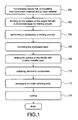
- the method for manufacturing a tag integrated circuit flexible board of the present invention comprises the steps as follows. Please also refer to Fig. 2A , first, in step 100, copper foil 1, an insulating heat-conductive material 2 and a base material 3 coated with an adhesive layer 31 are prepared. After being treated by a hot-pressing process, the copper foil 1, the insulating heat-conductive material 2 and the base material 3 are combined together to form a continuous band-like or sheet-like copper foil flexible board.
- the base material 3 is any one of a glue sheet or a thin metallic sheet.
- the thin metallic sheet can be any one of copper foil or aluminum foil.
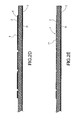
- step 102 with reference to Fig. 2B and Fig. 2C , the surface of the copper foil 1 is formed with a photoresist layer 4 for forming circuits thereon.
- step 104 with reference to Fig. 2D , after being treated by a developing or etching process, the portion of the copper foil 1 that is not covered with the photoresist layer 1 is etched off, while leaving the portion of the copper foil 1 that is covered with the photoresist layer 4.
- step 106 with reference to Fig. 2E and Fig. 2F , after removing the photoresist layer 4, on the copper foil 1, the plurality of sections of circuits 11 that are made by the developing or etching process are exposed to the surface of the insulating heat-conductive material 2 so as to form a conductive circuit layer.
- the plurality of sections of circuits can be also scribed by means of a laser process.
- step 108 with reference to Fig. 3 , the surface of the plurality of sections of circuits 11 are plated with a silver metallic layer 12.
- step 110 the surface of the silver metallic layer 12 is soldered with SMD electronic components 5.
- the electronic components 5 When the electronic components 5 are brought into contact with the silver metallic layer 12, after being heated, the electronic components 5 can be soldered with the silver metallic layer 12.
- the SMD electronic component 5 is any one of a semiconductor IC chip or a light-emitting chip of a light-emitting diode. Further, the silver metallic layer 12 can reflect the light generated by the light-emitting chip.
- step 112 with reference to Fig. 5 , the surface of the insulating heat-conductive material 2 is packaged with an outer covering body 6 to cover the SMD electronic components 5.
- step 120 with reference to Fig. 6 , the band-like or sheet-like copper foil flexible board is cut.
- the insulating heat-conductive material 2 is cut to form cutting seams 21 thereon while the base material 3 is not cut.
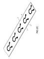
- the electronic elements 10 on the band-like or sheet-like base material 3 form a plurality of adjacent elements that are adhered on the base material 3.
- the packaging of the tag electronic elements is completed.
- FIG. 7 it is a schematic view showing an operating state in which the packaging of electronic elements is finished on the tag integrated circuit flexible board of the present invention.
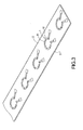
- the insulating heat-conductive material 2 is peeled off, so that the insulating heat-conductive material 2 can be peeled from the adhesive of the base material 3.
- the back of the insulating heat-conductive material 2 is adhesive slightly, so that the insulating heat-conductive material 2 can be adhered on the associated carriers.
- FIG. 8 it is a schematic view showing another operating state in which the packaging of electronic elements is finished on the tag integrated circuit flexible board of the present invention.
- the insulating heat-conductive material 2 is peeled from the base material, so that the insulating heat-conductive material 2 can be adhered on an isothermal plate 20.
- the insulating heat-conductive material 2 of the integrated circuit flexible board can be combined with the isothermal plate 20.
- the user can peel off the electronic elements from the base material when he intends to use the electronic elements. Also, after the manufacturing of the tag electronic elements is finished, the thus-manufactured electronic elements are easy to fold and carry. Furthermore, the plurality of electronic elements can be avoided from being pressed or damaged when carried. Also, the package volume can be made smaller to facilitate the carry.
Landscapes
- Engineering & Computer Science (AREA)
- Manufacturing & Machinery (AREA)
- Microelectronics & Electronic Packaging (AREA)
- Structure Of Printed Boards (AREA)
- Wire Bonding (AREA)
- Manufacturing Of Printed Circuit Boards (AREA)
- Structures For Mounting Electric Components On Printed Circuit Boards (AREA)
Applications Claiming Priority (1)
| Application Number | Priority Date | Filing Date | Title |
|---|---|---|---|
| TW096117722A TW200846250A (en) | 2007-05-18 | 2007-05-18 | Manufacture method of tag-typed integrated soft circuit board and a structure thereof |
Publications (2)
| Publication Number | Publication Date |
|---|---|
| EP1993333A2 true EP1993333A2 (fr) | 2008-11-19 |
| EP1993333A3 EP1993333A3 (fr) | 2010-03-31 |
Family
ID=39721960
Family Applications (1)
| Application Number | Title | Priority Date | Filing Date |
|---|---|---|---|
| EP08002193A Withdrawn EP1993333A3 (fr) | 2007-05-18 | 2008-02-06 | Procédé de fabrication de carte flexible de circuit à étiquette intégrée et structure correspondante |
Country Status (4)
| Country | Link |
|---|---|
| EP (1) | EP1993333A3 (fr) |
| JP (1) | JP2008288553A (fr) |
| KR (1) | KR20080101650A (fr) |
| TW (1) | TW200846250A (fr) |
Cited By (4)
| Publication number | Priority date | Publication date | Assignee | Title |
|---|---|---|---|---|
| WO2010136596A3 (fr) * | 2009-05-29 | 2011-02-03 | Brady Converting Ab | Procédé de fabrication d'un circuit électrique sur un substrat |
| CN102712138A (zh) * | 2010-01-21 | 2012-10-03 | Jx日矿日石金属株式会社 | 覆铜层压板的制备方法、其所使用的铜箔及覆铜层压板的层压装置 |
| CN106711085A (zh) * | 2016-12-12 | 2017-05-24 | 东莞市广信知识产权服务有限公司 | 一种柔性互连金属的制备方法 |
| CN113212892A (zh) * | 2021-05-12 | 2021-08-06 | 深圳市奥尼电通有限公司 | 一种半导体检测编带工艺及系统 |
Families Citing this family (4)
| Publication number | Priority date | Publication date | Assignee | Title |
|---|---|---|---|---|
| KR101419200B1 (ko) | 2014-02-10 | 2014-07-14 | 세종머티리얼즈 주식회사 | 플렉서블 인쇄회로기판의 제조방법 |
| CN105578788A (zh) * | 2015-12-31 | 2016-05-11 | 江西凯强实业有限公司 | 一种背光源挠性印制板的制作方法 |
| CN111263517A (zh) * | 2018-11-30 | 2020-06-09 | 群创光电股份有限公司 | 可挠性电路板的制造方法 |
| KR102198428B1 (ko) * | 2020-04-20 | 2021-01-05 | 주식회사 디엔엑스 | 사물부착 무선 태그 장치 |
Citations (4)
| Publication number | Priority date | Publication date | Assignee | Title |
|---|---|---|---|---|
| EP1028483A1 (fr) * | 1999-02-10 | 2000-08-16 | Allgon Ab | Circuit imprimé avec un motif conducteur pour équipement de radiocommunication et méthode de fabrication d'un tel circuit |
| US6482490B1 (en) * | 1999-02-10 | 2002-11-19 | Matsushita Electric Industrial Co., Ltd. | Printing sheet with base material, and method of manufacturing the same |
| EP1473978A1 (fr) * | 2002-01-24 | 2004-11-03 | Yuan Lin | Bande lumineuse et méthode de fabrication d'une telle lampe |
| WO2006132271A1 (fr) * | 2005-06-08 | 2006-12-14 | Minebea Co., Ltd. | Illuminateur de surface |
Family Cites Families (6)
| Publication number | Priority date | Publication date | Assignee | Title |
|---|---|---|---|---|
| JPS60109294A (ja) * | 1983-11-18 | 1985-06-14 | ソニー株式会社 | フレキシブル回路基板の製造方法 |
| JP2590566B2 (ja) * | 1989-07-11 | 1997-03-12 | 富士通株式会社 | フレキシブルプリント基板への電子部品の実装方法 |
| EP1742294B8 (fr) * | 1999-02-10 | 2010-12-22 | AMC Centurion AB | Procédé et dispositif pour la fabrication d'un rouleau d'articles |
| JP3561209B2 (ja) * | 2000-05-24 | 2004-09-02 | 株式会社三井ハイテック | フリップチップ実装用バインダー及びこれを用いた半導体装置の製造方法 |
| JP3659133B2 (ja) * | 2000-06-23 | 2005-06-15 | セイコーエプソン株式会社 | 半導体装置の製造方法 |
| JP2002232197A (ja) * | 2001-02-06 | 2002-08-16 | Matsushita Electric Ind Co Ltd | 電子部品実装方法 |
-
2007
- 2007-05-18 TW TW096117722A patent/TW200846250A/zh unknown
-
2008
- 2008-02-06 EP EP08002193A patent/EP1993333A3/fr not_active Withdrawn
- 2008-02-12 JP JP2008029992A patent/JP2008288553A/ja active Pending
- 2008-03-11 KR KR1020080022539A patent/KR20080101650A/ko not_active Application Discontinuation
Patent Citations (4)
| Publication number | Priority date | Publication date | Assignee | Title |
|---|---|---|---|---|
| EP1028483A1 (fr) * | 1999-02-10 | 2000-08-16 | Allgon Ab | Circuit imprimé avec un motif conducteur pour équipement de radiocommunication et méthode de fabrication d'un tel circuit |
| US6482490B1 (en) * | 1999-02-10 | 2002-11-19 | Matsushita Electric Industrial Co., Ltd. | Printing sheet with base material, and method of manufacturing the same |
| EP1473978A1 (fr) * | 2002-01-24 | 2004-11-03 | Yuan Lin | Bande lumineuse et méthode de fabrication d'une telle lampe |
| WO2006132271A1 (fr) * | 2005-06-08 | 2006-12-14 | Minebea Co., Ltd. | Illuminateur de surface |
Cited By (5)
| Publication number | Priority date | Publication date | Assignee | Title |
|---|---|---|---|---|
| WO2010136596A3 (fr) * | 2009-05-29 | 2011-02-03 | Brady Converting Ab | Procédé de fabrication d'un circuit électrique sur un substrat |
| CN102712138A (zh) * | 2010-01-21 | 2012-10-03 | Jx日矿日石金属株式会社 | 覆铜层压板的制备方法、其所使用的铜箔及覆铜层压板的层压装置 |
| CN106711085A (zh) * | 2016-12-12 | 2017-05-24 | 东莞市广信知识产权服务有限公司 | 一种柔性互连金属的制备方法 |
| CN106711085B (zh) * | 2016-12-12 | 2019-02-19 | 东莞市广信知识产权服务有限公司 | 一种柔性互连金属的制备方法 |
| CN113212892A (zh) * | 2021-05-12 | 2021-08-06 | 深圳市奥尼电通有限公司 | 一种半导体检测编带工艺及系统 |
Also Published As
| Publication number | Publication date |
|---|---|
| JP2008288553A (ja) | 2008-11-27 |
| TW200846250A (en) | 2008-12-01 |
| EP1993333A3 (fr) | 2010-03-31 |
| KR20080101650A (ko) | 2008-11-21 |
Similar Documents
| Publication | Publication Date | Title |
|---|---|---|
| EP1993333A2 (fr) | Procédé de fabrication de carte flexible de circuit à étiquette intégrée et structure correspondante | |
| CN102548253B (zh) | 多层电路板的制作方法 | |
| US9210811B2 (en) | Compact rigid-flexible printed circuit board and method for manufacturing same | |
| US9577169B2 (en) | LED lead frame for laminated LED circuits | |
| US20110079349A1 (en) | Method of manufacturing printed circuit board | |
| US20140085833A1 (en) | Chip packaging substrate, method for manufacturing same, and chip packaging structure having same | |
| CN103681384A (zh) | 芯片封装基板和结构及其制作方法 | |
| US20020127837A1 (en) | Methods for forming a die package | |
| US20180033763A1 (en) | Package substrate and manufacturing method thereof and package | |
| US7705461B2 (en) | Structure of tag integrated circuit flexible board | |
| TW201524292A (zh) | 電子封裝件、封裝載板及此封裝載板的製造方法 | |
| JP2005303031A (ja) | 電子回路モジュールと多層電子回路モジュールおよびそれらの製造方法 | |
| CN101315899B (zh) | 标签式集成线路软板制作方法及其结构 | |
| US10629511B2 (en) | Heat dissipation substrate, manufacturing method thereof and chip package structure | |
| US9905519B1 (en) | Electronic structure process | |
| JP5968827B2 (ja) | 半導体パッケージおよびその製造方法 | |
| KR101898479B1 (ko) | 복수 캐리어 기판을 이용한 인쇄회로기판 제조 방법 | |
| CN108615686B (zh) | 芯片封装结构的制作方法与基板结构 | |
| CN114256169A (zh) | 半导体封装结构及其制备方法 | |
| JP2004087895A (ja) | パッケージ部品およびその製造方法 | |
| KR100529927B1 (ko) | 다중 칩 모듈 패키지 구조 및 그 제작방법 | |
| US20020151102A1 (en) | Stacked semiconductor package structure having films and method for manufacturing the films | |
| TWI364105B (en) | Mask plate for packaging chip module and encapsulation method using the same | |
| JP2003067708A (ja) | Icタグラベルの製造方法 | |
| US7122124B2 (en) | Method of fabricating film carrier |
Legal Events
| Date | Code | Title | Description |
|---|---|---|---|
| PUAI | Public reference made under article 153(3) epc to a published international application that has entered the european phase |
Free format text: ORIGINAL CODE: 0009012 |
|
| AK | Designated contracting states |
Kind code of ref document: A2 Designated state(s): AT BE BG CH CY CZ DE DK EE ES FI FR GB GR HR HU IE IS IT LI LT LU LV MC MT NL NO PL PT RO SE SI SK TR |
|
| AX | Request for extension of the european patent |
Extension state: AL BA MK RS |
|
| RAP1 | Party data changed (applicant data changed or rights of an application transferred) |
Owner name: PYROSWIFT HOLDING CO., LIMITED |
|
| PUAL | Search report despatched |
Free format text: ORIGINAL CODE: 0009013 |
|
| AK | Designated contracting states |
Kind code of ref document: A3 Designated state(s): AT BE BG CH CY CZ DE DK EE ES FI FR GB GR HR HU IE IS IT LI LT LU LV MC MT NL NO PL PT RO SE SI SK TR |
|
| AX | Request for extension of the european patent |
Extension state: AL BA MK RS |
|
| RIC1 | Information provided on ipc code assigned before grant |
Ipc: H05K 3/00 20060101ALI20080910BHEP Ipc: H05K 1/18 20060101ALI20080910BHEP Ipc: H05K 3/00 20060101AFI20100225BHEP |
|
| 17P | Request for examination filed |
Effective date: 20100416 |
|
| RIC1 | Information provided on ipc code assigned before grant |
Ipc: H05K 1/18 20060101ALI20100831BHEP Ipc: H05K 3/00 20060101AFI20100831BHEP |
|
| RTI1 | Title (correction) |
Free format text: METHOD FOR MANUFACTURING TAG INTEGRATED CIRCUIT FLEXIBLE BOARD |
|
| AKY | No designation fees paid | ||
| STAA | Information on the status of an ep patent application or granted ep patent |
Free format text: STATUS: THE APPLICATION HAS BEEN WITHDRAWN |
|
| 18W | Application withdrawn |
Effective date: 20100930 |
|
| REG | Reference to a national code |
Ref country code: DE Ref legal event code: R108 Effective date: 20110208 Ref country code: DE Ref legal event code: 8566 |