EP1959599A2 - Système de commutation sans à-coup et appareil de transmission - Google Patents
Système de commutation sans à-coup et appareil de transmission Download PDFInfo
- Publication number
- EP1959599A2 EP1959599A2 EP08157645A EP08157645A EP1959599A2 EP 1959599 A2 EP1959599 A2 EP 1959599A2 EP 08157645 A EP08157645 A EP 08157645A EP 08157645 A EP08157645 A EP 08157645A EP 1959599 A2 EP1959599 A2 EP 1959599A2
- Authority
- EP
- European Patent Office
- Prior art keywords
- virtual concatenation
- signals
- parts
- sending
- original signal
- Prior art date
- Legal status (The legal status is an assumption and is not a legal conclusion. Google has not performed a legal analysis and makes no representation as to the accuracy of the status listed.)
- Granted
Links
- 230000005540 biological transmission Effects 0.000 title claims abstract description 93
- 238000001514 detection method Methods 0.000 claims abstract description 18
- 238000005516 engineering process Methods 0.000 claims description 13
- 230000015654 memory Effects 0.000 description 51
- 238000000034 method Methods 0.000 description 14
- 238000010586 diagram Methods 0.000 description 12
- 230000001360 synchronised effect Effects 0.000 description 9
- 230000006870 function Effects 0.000 description 2
- 238000010521 absorption reaction Methods 0.000 description 1
- 238000004891 communication Methods 0.000 description 1
- 238000012986 modification Methods 0.000 description 1
- 230000004048 modification Effects 0.000 description 1
Images


Classifications
-
- H—ELECTRICITY
- H04—ELECTRIC COMMUNICATION TECHNIQUE
- H04J—MULTIPLEX COMMUNICATION
- H04J3/00—Time-division multiplex systems
- H04J3/02—Details
- H04J3/06—Synchronising arrangements
- H04J3/0602—Systems characterised by the synchronising information used
-
- H—ELECTRICITY
- H04—ELECTRIC COMMUNICATION TECHNIQUE
- H04J—MULTIPLEX COMMUNICATION
- H04J3/00—Time-division multiplex systems
- H04J3/02—Details
- H04J3/06—Synchronising arrangements
- H04J3/062—Synchronisation of signals having the same nominal but fluctuating bit rates, e.g. using buffers
-
- H—ELECTRICITY
- H04—ELECTRIC COMMUNICATION TECHNIQUE
- H04J—MULTIPLEX COMMUNICATION
- H04J3/00—Time-division multiplex systems
- H04J3/02—Details
- H04J3/14—Monitoring arrangements
-
- H—ELECTRICITY
- H04—ELECTRIC COMMUNICATION TECHNIQUE
- H04L—TRANSMISSION OF DIGITAL INFORMATION, e.g. TELEGRAPHIC COMMUNICATION
- H04L1/00—Arrangements for detecting or preventing errors in the information received
- H04L1/22—Arrangements for detecting or preventing errors in the information received using redundant apparatus to increase reliability
-
- H—ELECTRICITY
- H04—ELECTRIC COMMUNICATION TECHNIQUE
- H04J—MULTIPLEX COMMUNICATION
- H04J2203/00—Aspects of optical multiplex systems other than those covered by H04J14/05 and H04J14/07
- H04J2203/0001—Provisions for broadband connections in integrated services digital network using frames of the Optical Transport Network [OTN] or using synchronous transfer mode [STM], e.g. SONET, SDH
- H04J2203/0089—Multiplexing, e.g. coding, scrambling, SONET
- H04J2203/0094—Virtual Concatenation
Definitions
- the present invention relates to a hitless switching system. More particularly, the present invention relates to a hitless switching system for switching between signals transmitted over a plurality of routes in a synchronous digital transmission network including a plurality of nodes that have multiplexing/demultiplexing capability or cross connect capability.
- a signal is branched into two signals in the sending side, and the branched signals are sent over two different routes. Branched signals are the same. Then, in the receiving side, one signal is switched to another signal within one bit after aligning phases between the signals.
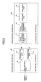
- Fig.1 shows a block diagram of a transmission system for explaining a conventional hitless switching technology.
- the system shown in Fig.1 includes a sending side apparatus and a receiving side apparatus.
- the sending side apparatus includes an indicator providing part 11, a branch part 12, a first sending interface 13, a second sending interface 14.
- the receiving side apparatus includes a first receiving interface 15, a second receiving interface 16, a first elastic store memory 17, a second elastic store memory 18, a phase control part 19, and a selector 20.
- the indicator providing part 11 receives a signal 101 to be switched with no bit error, and a signal 102 that is switched with no bit error is output from the selector 20.
- the signal 101 is provided with an indicator used for phase control in the indicator providing part 11. Then, the signal 101 is input into the branch part 12. After that, the signal 101 is branched into the first sending interface 13 and the second sending interface 14. Branched signals are the same. According to this process, sending data is sent to different two routes.
- the signal input into the first receiving interface 15 is stored in the first elastic store memory 17.
- the signal input into the second receiving interface 16 is stored in the second elastic store memory 18.
- Phases for reading the signals stored in the first elastic store memory 17 and the second elastic store memory 18 are aligned by the phase control part 19. Then, the signals are received by the selector 20.
- the selector 20 performs switching within one bit. In the switching, it is decided whether the selector 20 receives a signal from the first elastic store memory 17 or receives a signal from the second elastic store memory 18.
- the phase aligning between signals transmitted over different two routes are performed in the following way.
- the signals are temporarily stored in the elastic store memories.
- phase difference between the signals is detected by using a specific pattern (indicator) that has been inserted into J1 byte multi-frame or H4 byte multi-frame in each signal at the sending side, wherein each of the J1 byte multi-frame and the H4 byte multi-frame exists in POH in synchronous digital hierarchy defined in ITU-T G.707.
- the phases of the signals are aligned for reading from the elastic store memories.
- an original signal is divided into a plurality of virtual concatenation signals in the sending side. Then, phases are aligned between signals that are transmitted over the same route or over different routes. After that, the original signal is restored.
- Fig.2 shows a block diagram of a transmission system for explaining the virtual concatenation technology.
- the system shown in Fig.2 includes a sending side apparatus and a receiving side apparatus.
- the sending side apparatus includes a distributing part 31, indicator providing parts 32 1 ⁇ 32 n , sending interfaces 33 1 ⁇ 33 n .
- the receiving side apparatus includes receiving interfaces 34 1 ⁇ 34 n , elastic store memories 35 1 ⁇ 35 n , a phase control part 36, and a restoring part 37.
- the distributing part 31 receives a signal 201 to which virtual concatenation is to be applied.
- the signal 201 is divided and transmitted.
- a restored signal 202 is output from the restoring part 37.
- the signal 201 is divided into a plurality of virtual concatenation signals in the distributing part 31. Then, an indicator used for phase control is provided to each virtual concatenation signal in the indicator providing parts 32 1 ⁇ 32 n . After that, the virtual concatenation signals are input into the sending interfaces 33 1 ⁇ 33 n so as to be transmitted over the same route or different routes.
- the virtual concatenation signals received by the receiving interfaces 34 1 ⁇ 34 n are stored in the elastic store memories 35 1 ⁇ 35 n .
- Phases for reading the virtual concatenation signals stored in the elastic store memories 35 1 ⁇ 35 n are aligned by the phase control part 36. Then, the virtual concatenation signals are input into the restoring part 37 so that the original signal is restored.
- the phase aligning between the virtual concatenation signals is performed in the following way.
- the virtual concatenation signals which are transmitted over the same route or the different routes are temporarily stored in the elastic store memories.
- phase difference between signals are detected by using a specific pattern (indicator) that has been inserted, at the sending side, into the H4 byte multi-frame in POH of each signal, wherein the H4 byte multi-frame is defined in ITU-T G.707.
- the phases of the signals are aligned when reading from the elastic store memories.
- the J1 byte multi-frame is used for detecting phase difference between signals transmitted over different two routes, there is a problem since the J1 byte is defined as a path trace byte used for uniquely detecting a path in the synchronous digital hierarchy in ITU-T G.707.
- the path trace can not be realized, so that the hitless switching and the path trace can not be compatible.
- the H4 byte multi-frame in POH is used for detecting the phase difference
- the H4 byte multi-frame used for hitless switching overwrites the H4 byte multi-frame used for virtual concatenation since the H4 byte is defined as a byte used for detecting phase difference for realizing virtual concatenation. Therefore, in this case, the original signal can not be restored from the divided virtual concatenation signals, so that the hitless switching and the virtual concatenation can not be compatible.
- An object of the present invention is to provide a hitless switching system and a transmission apparatus, without increasing complexity of the system and the apparatus, to support signals of large capacity accompanying increase of recent LAN traffic, and to support signals of intermediate bandwidth corresponding to virtual concatenations such as VC-3-Xv (50xX Mbit/s (X is an integer of 1 ⁇ 256)) and VC-4-Xv (150xX Mbit/s (X is an integer of 1 ⁇ 256)) other than VC-3, VC-4 and VC-4-Xc(X is 4, 16, 64 or 256).
- a hitless switching system for switching between signals transmitted over a plurality of transmission lines
- the hitless switching system including a sending apparatus and a receiving apparatus, the sending apparatus including:
- the original signal is divided into n signals for example, and 2n branched signals, for example, are sent to a receiving side over transmission lines. Then, switching is performed after phase differences of the 2n signals are absorbed. Therefore, absorption of phase differences for dividing and restoring signals and for redundancy switching can be carried out at a time. In addition, since the original signal is divided into n signals, hitless switching of intermediate bandwidth can be realized.
- the sending apparatus further includes branch parts each of which branches one of the divided signals into a first signal and a second signal, wherein the transmitting part transmits first signals and second signals, the receiving apparatus aligns phases of the first signals and the second signals, and provides the first signals and the second signals to the selectors.
- the hitless switching system includes, in place of the selectors and the restoring part:
- the sending apparatus further includes:
- a protection transmission line (transmitting second signal) can be commonly used by a plurality of working transmission lines (transmitting first signal), so that communication resources can be used effectively.
- the distributing part includes:
- VC-3-Xv 50xX Mbit/s (X is an integer of 1 ⁇ 256)
- VC-4-Xv 150xX Mbit/s (X is an integer of 1 ⁇ 256)
- phase alignment for hitless switching and phase alignment for virtual concatenation can be performed at the same time.
- complexity of the apparatuses in the system increases and increase of delay can be avoided.
- virtual concatenation can be compatible with hitless switching, and path trace by J1 byte can be compatible with hitless switching.
- a transmission apparatus for switching between signals transmitted over transmission lines including:
- the transmission apparatus includes, instead of the selectors and the restoring part:
- the transmission apparatus includes a branch part for branching one virtual concatenation signal of the received virtual concatenation signals into a plurality of virtual concatenation signals that are supplied to the selectors.
- the hitless switching system in the embodiments of the present invention is an example of a synchronous digital transmission system having capabilities of synchronous digital hierarchy and virtual concatenation defined in ITU-T G.707.
- the virtual concatenation technology in the embodiments and H4 byte multi-frame used for detecting phase difference of the virtual concatenation signals are defined in ITU-T G.707.
- Fig.3 shows a principle block diagram of the hitless switching system according to the embodiments of the present invention.
- the hitless switching system includes a sending side apparatus 40 and a receiving side apparatus 50.
- the sending side apparatus 40 includes a distributing part 41, transmitting parts 42.
- the distributing part 41 divides an original signal into a plurality of signals.
- the transmitting parts 42 transmits the divided signals over one route or a plurality of routes.
- the receiving side apparatus 50 includes a phase difference detection part 51, a phase difference absorbing part 52, a switching part 53, and a restoring part 54.
- the phase difference detection part 51 detects phase difference between signals transmitted over one route or over a plurality of routes.
- the phase difference absorbing part 52 absorbs phase difference detected by the phase difference detection part 51.
- the switching part 53 switches between signals with no bit error.
- the restoring part 54 restores the original signal from the divided signals.
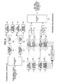
- Fig.4 is a block diagram of the hitless switching system according to the first embodiment of the present invention.
- the configuration shown in the figure is for realizing hitless switching function using virtual concatenation defined-in ITU-T G.707.
- the sending side apparatus includes a distributing part 212, indicator providing parts 220 1 ⁇ 220 n , branch parts 230 1 ⁇ 230 n , first sending interfaces 240 1 ⁇ 240 n , and second sending interfaces 250 1 ⁇ 250 n .
- the distributing part 212 divides the original signal into a plurality of virtual concatenation signals defined in ITU-T G.707.
- Each of the indicator providing parts 220 1 ⁇ 220 n provides H4 byte multi-frame to the virtual concatenation signal for detecting phase difference between virtual concatenation signals.
- Each of the branch parts 230 1 ⁇ 230 n branches the virtual concatenation signal into two systems.
- Each of the first sending interfaces 240 1 ⁇ 240 n transmits one of the branched virtual concatenation signals to a first transmission line.
- Each of the second sending interfaces 250 1 ⁇ 250 n transmits one of the branched virtual concatenation signals to a second transmission line.
- the first transmission lines and the second transmission lines can be one route or a plurality of routes. This applies also to other embodiments.
- the receiving side apparatus of the hitless switching system includes first receiving interfaces 260 1 ⁇ 260 n for receiving virtual concatenation signals from first transmission lines, second receiving interfaces 270 1 ⁇ 270 n for receiving virtual concatenation signals from the second transmission lines, first elastic store memories 280 1 ⁇ 280 n , second elastic store memories 290 1 ⁇ 290 n , a phase control part 210, selectors 211 1 ⁇ 211 n , and a restoring part 213.
- the selectors 211 1 ⁇ 211 n corresponds to the switching part 53 in Fig.3 .
- the first elastic store memories 280 1 ⁇ 280 n are for temporarily storing virtual concatenation signals received from the first transmission lines.
- the second elastic store memories 290 1 ⁇ 290 n are for temporarily storing virtual concatenation signals received from the second transmission lines.
- the phase control part 210 detects phase difference between virtual concatenation signals that are transmitted over different routes and aligns phases for reading virtual concatenation signals from each elastic store memory.
- Each of the selectors 211 1 ⁇ 211 n performs switching between a virtual concatenation signal received from the first transmission line and a virtual concatenation signal received from the second transmission line.
- the restoring part 213 restores the original signal from the virtual concatenation signals in conformity with ITU-T G.707.
- the original signal 200 to which hitless switching is to be applied is received by the distributing part 212.
- the distributing part 212 divides the original signal into a plurality of virtual concatenation signals.
- each of the indicator providing part 220 1 ⁇ 220 n writes a specific pattern (indicator) in the H4 byte multi-frame of the virtual concatenation signal, in which the specific pattern is used for detecting phase difference for restoring the divided signals into the original signal and is used for detecting phase difference for hitless switching, however, the phase differences are not distinguished.
- the original signal is divided into the virtual concatenation signals.
- the original signal (A) is divided into n signals which can be represented as A1 ,A2 ,...,An.
- A1 is sent to the indicator providing part 220 1 .
- An is sent to the indicator providing part 220 n .
- each of the virtual concatenation signals from the indicator providing part 220 1 ⁇ 220 n is branched into two different systems by the branch part 230 1 ⁇ 230 n .
- One of the branched signals is sent to the first transmission line by corresponding one of the first sending interfaces 240 1 ⁇ 240 n .
- Another one of the branched signals is sent to the second transmission line by corresponding one of the second sending interfaces 250 1 ⁇ 250 n .
- the virtual concatenation signals sent over the first transmission lines are transmitted to the first receiving interfaces 260 1 ⁇ 260 n via the synchronous digital transmission network.
- the virtual concatenation signals sent over the second transmission lines are transmitted to the second receiving interfaces 270 1 ⁇ 270 n via the synchronous digital transmission network.
- Each signal sent from the first sending interface is the same as the signal sent from the corresponding second sending interface.
- the first receiving interfaces 260 1 ⁇ 260 n receive virtual concatenation signals sent over the first transmission lines
- the second receiving interfaces 270 1 ⁇ 270 n receive virtual concatenation signals sent over the second transmission lines.
- the virtual concatenation signals received from the first transmission lines are temporarily stored in the first elastic store memories 280 1 ⁇ 280 n
- the virtual concatenation signals received from the second transmission lines are temporarily stored in the second elastic store memories 290 1 ⁇ 290 n .
- the phase control part 210 detects phase differences on the basis of the specific pattern (indicator) written in the H4 byte multi-frame.
- the virtual concatenation signals are sent to the selectors 211 1 ⁇ 211 n .
- switching of selection system is performed within one bit between the virtual concatenation signal received from the first transmission line and the virtual concatenation signal received from the second transmission line.
- the switching means that each of the selectors 211 1 ⁇ 211 n selects between receiving a signal from the first elastic store memory or receiving a signal from the second elastic store memory.
- the virtual concatenation signals in which switching of selection system is performed by the selectors 211 1 ⁇ 211 n are sent to the restoring part 213, so that the original signal is restored.
- one branch part is provided to each virtual concatenation signal in the sending side, and one selector is provided to each virtual concatenation signal in the receiving side.
- the branch parts 230 1 ⁇ 230 n can be replaced by a switch for branching the virtual concatenation signals.
- the selectors 211 1 ⁇ 211 n can be replaced by a switch for selecting between virtual concatenation signals.
- the branch part 230 is located after the distributing part 212 in the sending side, and the selector 211 is located before the restoring part 213.
- the hitless switching can be also realized by a configuration in which the original signal is branched into two systems before dividing into virtual concatenation signals in the sending side, and switching is performed after restoring the original signal.
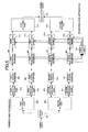
- Fig.5 is a block diagram of the hitless switching system according to the second embodiment of the present invention.
- the sending side apparatus includes a branch part 310, a first distributing part 320 1 , a second distributing part 320 2 , first indicator providing parts 340 1 ⁇ 340 n , second indicator providing parts 350 1 ⁇ 350 n , first sending interfaces 360 1 ⁇ 360 n , and second sending interfaces 370 1 ⁇ 370 n .
- the branch part 310 branches the original signal into two systems.
- the first distributing part 320 1 divides one original signal in the branched original signals (which will be referred to as first original signal in the following) into a plurality of virtual concatenation signals according to the standard of virtual concatenation defined in ITU-T G.707.
- the second distributing part 320 2 divides another original signal (which will be referred to as second original signal in the following) into a plurality of virtual concatenation signals according to the standard of virtual concatenation defined in ITU-T G.707.
- Each of the first indicator providing parts 340 1 ⁇ 340 n provides H4 byte multi-frame to the virtual concatenation signal divided from the first original signal for detecting phase difference between virtual concatenation signals.
- Each of the second indicator providing parts 350 1 ⁇ 350 n provides H4 byte multi-frame to the virtual concatenation signal divided from the second original signal for detecting phase difference between virtual concatenation signals.
- the phase difference includes phase difference caused by dividing the original signal into virtual concatenation signals and sending the virtual concatenation signals and phase difference caused by sending the virtual concatenation signals over different routes.
- Each of the first sending interfaces 360 1 ⁇ 360 n transmits one of the divided virtual concatenation signals divided from the first original signal to a first transmission line.
- Each of the second sending interfaces 370 1 ⁇ 370 n transmits one of the divided virtual concatenation signals divided from the second original signal to a second transmission line.
- the receiving side apparatus of the hitless switching system includes first receiving interfaces 380 1 ⁇ 380 n for receiving virtual concatenation signals from first transmission lines, second receiving interfaces 390 1 ⁇ 390 n for receiving virtual concatenation signals from the second transmission lines, first elastic store memories 311 1 ⁇ 311 n , second elastic store memories 312 1 ⁇ 312 n , a phase control part 314, a first restoring part 313 1 , a second restoring part 313 2 , and a selector 315.
- the first elastic store memories 311 1 ⁇ 311 n are for temporarily storing virtual concatenation signals received from the first transmission lines.
- the second elastic store memories 312 1 ⁇ 312 n are for temporarily storing virtual concatenation signals received from the second transmission lines.
- the phase control part 314 detects phase differences among all virtual concatenation signals and aligns phases for reading virtual concatenation signals from each elastic store memory.
- the first restoring part 313 1 restores the first original signal from the virtual concatenation signals read from the first elastic store memories 311 1 ⁇ 311 n .
- the second restoring part 313 2 restores the second original signal from the virtual concatenation signals read from second elastic store memories 312 1 ⁇ 312 n .
- the selector 315 performs switching between the first original signal and the second original signal.
- the original signal 200 to which hitless switching is to be applied is received by the dividing part 310. Then, the original signal is branched into the first original signal and the second original signal. After that, the first original signal is received by the first distributing part 320 1 , and the second original signal is received by the second distributing part 320 2 . The first original signal and the second original signal are the same.
- the first distributing part 320 1 divides the first original signal into a plurality of virtual concatenation signals.
- each of the first indicator providing part 340 1 ⁇ 340 n writes a specific pattern (indicator) in the H4 byte multi-frame of the virtual concatenation signal, in which the specific pattern is used for detecting phase difference for restoring the divided signals into the original signal and is used for detecting phase difference for hitless switching.
- the virtual concatenation signals are sent to the first transmission lines from the first sending interfaces 360 1 ⁇ 360 n .
- the second distributing part 320 2 divides the second original signal into a plurality of virtual concatenation signals. After that, each of the second indicator providing part 350 1 ⁇ 350 n writes a specific pattern (indicator) in the H4 byte multi-frame of the virtual concatenation signal, in which the specific pattern is used for detecting phase difference for restoring the divided signals into the original signal and is used for detecting phase difference for hitless switching. Then, the virtual concatenation signals are sent to the second transmission lines from the second sending interfaces 370 1 ⁇ 370 n .
- the original signal is divided into the first virtual concatenation signals and second virtual concatenation signals.
- the first receiving interfaces 380 1 ⁇ 380 n receive the first virtual concatenation signals sent over the first transmission lines
- the second receiving interfaces 390 1 ⁇ 390 n receive the second virtual concatenation signals sent over the second transmission lines.
- the first virtual concatenation signals received from the first transmission lines are temporarily stored in the first elastic store memories 311 1 ⁇ 311 n
- the second virtual concatenation signals received from the second transmission lines are temporarily stored in the second elastic store memories 312 1 ⁇ 312 n .
- the phase control part 314 detects phase differences among all virtual concatenation signals on the basis of the specific pattern (indicator) written in the H4 byte multi-frame, so that phases for reading the virtual concatenation signals are aligned.
- the first virtual concatenation signals are sent to the first restoring part 313 1 , so that the first original signal is restored.
- the first original signal is sent to the selector 315.
- the second virtual concatenation signals are sent to the second restoring part 313 2 , so that the second original signal is restored.
- the second original signal is sent to the selector 315.
- the selector 315 performs switching of selection system within one bit between the first original signal and the second original signal.
- Hitless switching can be also realized by a combination of the sending side apparatus of the first embodiment and the receiving side apparatus of the second embodiment, or a combination of the sending side apparatus of the second embodiment and the receiving side apparatus of the first embodiment.
- redundancy is realized by using the first system and the second system for every virtual concatenation signal divided from the original signal.
- the second transmission line is commonly used by a plurality of first transmission lines. Signals are sent to the first sending interfaces and one of the signal is also sent to the second sending interface. According to this embodiment, signals can be transmitted efficiently by using one second sending interface and a plurality of first sending interfaces.
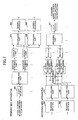
- Fig.6 is a block diagram of the hitless switching system according to the third embodiment of the present invention.
- the configuration shown in the figure is for realizing hitless switching function using virtual concatenation defined in ITU-T G.707.
- the sending side apparatus includes a distributing part 410, indicator providing parts 420 1 ⁇ 420 n , branch parts 430 1 ⁇ 430 n , a selector 440, a first sending interfaces 450 1 ⁇ 450 n , and a second sending interface 460.
- the distributing part 410 divides the original signal into a plurality of virtual concatenation signals defined in ITU-T G.707.
- Each of the indicator providing parts 420 1 ⁇ 420 n provides H4 byte multi-frame to the virtual concatenation signal for detecting phase difference between virtual concatenation signals, in which the phase difference includes phase difference caused by dividing the original signals into virtual concatenation signals and sending the virtual concatenation signals and phase difference caused by sending the virtual concatenation signals over different routes.
- Each of the branch parts 430 1 ⁇ 430 n branches the virtual concatenation signal into a first virtual concatenation signal and a second virtual concatenation signal.
- the selector 440 selects a second virtual concatenation signal used for hitless switching from a plurality of second virtual concatenation signals.
- Each of the first sending interfaces 450 1 ⁇ 450 n transmits one of the divided virtual concatenation signals to a first transmission line.
- the second sending interface 460 transmits the second virtual concatenation signal to a second transmission line.
- the receiving side apparatus of the hitless switching system includes first receiving interfaces 470 1 ⁇ 470 n for receiving first virtual concatenation signals from first transmission lines, a second receiving interface 480 for receiving a second virtual concatenation signal from the second transmission line, first elastic store memories 490 1 ⁇ 490 n , a second elastic store memory 485, a phase control part 411, a branch part 412, selectors 413 1 ⁇ 413 n , and a restoring part 414.
- the first elastic store memories 490 1 ??490 n are for temporarily storing the first virtual concatenation signals received from the first transmission lines.
- the second elastic store memory 480 is for temporarily storing the second virtual concatenation signal received from the second transmission line.
- the phase control part 411 detects phase differences among all virtual concatenation signals that are transmitted over different routes and aligns phases for reading signals from each elastic store memory.
- the branch part 412 is for branching the second virtual concatenation signal into a plurality of second virtual concatenation signals.
- Each of the selectors 413 1 ⁇ 413 n performs switching between the first virtual concatenation signal and the second virtual concatenation signal.
- the restoring part 414 restores the original signal from the selected virtual concatenation signals.
- the original signal 410 to which hitless switching is to be applied is received by the distributing part 410.
- the distributing part 410 divides the original signal into a plurality of virtual concatenation signals. After that, each of the indicator providing part 420 1 ⁇ 420 n writes a specific pattern (indicator) in the H4 byte multi-frame of the virtual concatenation signal. According to this process, the original signal is divided into the virtual concatenation signals.
- each of the virtual concatenation signals from the indicator providing parts 420 1 ⁇ 420 n is branched into the first virtual concatenation signal and the second virtual concatenation signal by the branch parts 430 1 ⁇ 430 n .
- the branched first virtual concatenation signals are sent to the first sending interfaces 450 1 ⁇ 450 n .
- the branched second virtual concatenation signals are sent to the selector 440.
- the selector 440 selects a virtual concatenation signal that is to be used for hitless switching from a plurality of second virtual concatenation signals.
- the selected second virtual concatenation signal is sent to the second sending interface 460.
- the first receiving interfaces 470 1 ⁇ 470 n receive the first virtual concatenation signals
- the second receiving interface 480 receives the second virtual concatenation signal.
- the first virtual concatenation signals are temporarily stored in the first elastic store memories 490 1 ⁇ 490 n
- the second virtual concatenation signal is temporarily stored in the second elastic store memory 485.
- the phase control part 411 detects phase differences on the basis of the specific pattern (indicator) written in the H4 byte multi-frame.
- the first virtual concatenation signals are sent to the selectors 413 1 ⁇ 413 n .
- the second virtual concatenation signal is sent to the branch part 412 and branched and sent to each of the selectors 413 1 ⁇ 413 n .
- each of the selectors 413 1 ⁇ 413 n that receives the first and second virtual concatenation signals switching of selection system is performed within one bit between the first virtual concatenation signal and the second virtual concatenation signal.
- the virtual concatenation signals in which switching of selection system is performed by the selectors 413 1 ⁇ 413 n are sent to the restoring part 414, so that the original signal is restored.
- a selector that receives a first virtual concatenation signal other than a first virtual concatenation signal to be switched fixes the selector to avoid erroneous switching, so that it sends the received first virtual concatenation signal to the restoring part 414.
- the restoring part 414 restores the original signal from the input virtual concatenation signals.
- the specific pattern used for detecting phase differences for hitless switching in the first to third embodiments is H4 byte 4096 multi-frame used for detecting phase differences among a plurality of virtual concatenation signals in virtual concatenation defined in ITU-T G.707.
- the elastic store memories for aligning virtual concatenation signals transmitted over different routes are elastic store memories for aligning phases among a plurality of virtual concatenation signals.
- the present invention is a hitless switching system in which switching among signals sent over a plurality of different routes.
- the number of routes over which the divided virtual concatenation signals are sent is not limited to two.
- the virtual concatenation signals can be transmitted over a plurality of different routes.
- the hitless switching system is based on a synchronous digital transmission system having synchronous digital hierarchy and virtual concatenation capability defined by ITU-T G.707 as an example.
- the hitless switching system of the present invention can be also configured by including multiplexers, cross connect apparatuses and add-drop multiplexers and the like.
- Figs.7-9 shows a multiplexer, an add-drop multiplexer and a cross connect apparatus as an example of a transmission apparatus having the hitless switching capability of the present invention.
- Fig.7 shows an example of a system including multiplexers with the hitless switching capability.
- the multiplexer in the sending side includes multiplexing parts 510 and 520 and sending interfaces 530 and 540 in place of the sending interfaces 240 and 250 in the first embodiment.
- the multiplexer includes a client interface 590 for receiving a client signal.
- signals branched by the branch parts are multiplexed in the multiplexing parts 510 and 520, and output from the sending interfaces 530 and 540.
- the multiplexer (demultiplexer) in the receiving side includes receiving interfaces 550 and 560 and demultiplexing parts 570 and 580 in place of the receiving interfaces 260 and 270 in the first embodiment. In addition, it includes a client interface 595 for outputting the client signal.
- signals sent from the sending interfaces 530 and 540 are received by the receiving interfaces 550 and 560, and the demultiplexing parts 570 and 580 demultiplexes the multiplexed signals. Processes for hitless switching are the same as those of the first embodiment.
- Fig.8 shows an example of a system including add-drop multiplexers with the hitless switching capability of the present invention.
- the add-drop multiplexer in the sending side includes a SW (switching) part 600, multiplexing parts 610, 615 and sending interfaces 620, 625 in place of the sending interfaces 240 and 250 in the first embodiment.
- the add-drop multiplexer includes a client interface 660 for receiving a client signal.
- signals are switched by the SW part for realizing add-drop and sent to the multiplexing parts 610, 615. Signals are multiplexed in the multiplexing parts 610, 615, and output from the sending interfaces 620, 625.
- the add-drop multiplexer in the receiving side includes receiving interfaces 630, 635, demultiplexing parts 640, 645 and a SW part 650 in place of the receiving interfaces 260 and 270 in the first embodiment.
- it includes a client interface 665 for outputting the client signal.
- signals sent from the sending interfaces 620, 625 are received by the receiving interfaces 630, 635, and the demultiplexing parts 640, 645 demultiplexes the multiplexed signals.
- the SW part 650 switches routes of the signals. Processes for hitless switching are the same as those of the first embodiment.
- Fig.9 shows an example of a system including cross connect apparatuses with the hitless switching capability of the present invention.
- the cross connect apparatus in the sending side includes a SW part 710 between the branch part 230 and the sending interfaces 240, 250 in the first embodiment.
- the cross connect apparatus includes a client interface 730 for receiving a client signal.
- routes of signals are switched by the SW part 710, and the signals are sent to the sending interfaces.
- the cross connect apparatus in the receiving side includes a SW part 720 between the receiving interfaces 260, 270 and the elastic store memories 280, 290. In addition, it includes a client interface 740 for outputting the client signal.
- signals sent from the sending interfaces are received by the receiving interfaces, and the SW part 720 switches the routes of the signals. Processes for hitless switching are the same as those of the first embodiment.
- phase differences among the first virtual concatenation signals and the second virtual concatenation signals transmitted over a plurality of different routes are detected by using the H4 byte multi-frame in virtual concatenation defined in ITU-T G.707. Then, the elastic store memories absorb the phase differences. Therefore, hitless switching can be realized for signals of intermediate bandwidth corresponding to virtual concatenation such as VC-3-Xv (50xX Mbit/s (X is an integer of 1 ⁇ 256)) and VC-4-Xv (150xX Mbit/s (X is an integer of 1 ⁇ 256)) other than VC-3, VC-4 and VC-4-Xc(X is 4, 16, 64 or 256).
- virtual concatenation can be compatible with hitless switching, and path trace by J1 byte can be compatible with hitless switching.
Landscapes
- Engineering & Computer Science (AREA)
- Computer Networks & Wireless Communication (AREA)
- Signal Processing (AREA)
- Computer Hardware Design (AREA)
- Detection And Prevention Of Errors In Transmission (AREA)
- Time-Division Multiplex Systems (AREA)
- Data Exchanges In Wide-Area Networks (AREA)
Applications Claiming Priority (2)
| Application Number | Priority Date | Filing Date | Title |
|---|---|---|---|
| JP2002056320 | 2002-03-01 | ||
| EP03251201A EP1341329B1 (fr) | 2002-03-01 | 2003-02-27 | Système et dispositif de transmission à commutation sans perturbation |
Related Parent Applications (2)
| Application Number | Title | Priority Date | Filing Date |
|---|---|---|---|
| EP03251201.4 Division | 2003-02-27 | ||
| EP03251201A Division EP1341329B1 (fr) | 2002-03-01 | 2003-02-27 | Système et dispositif de transmission à commutation sans perturbation |
Publications (3)
| Publication Number | Publication Date |
|---|---|
| EP1959599A2 true EP1959599A2 (fr) | 2008-08-20 |
| EP1959599A3 EP1959599A3 (fr) | 2008-12-03 |
| EP1959599B1 EP1959599B1 (fr) | 2011-07-13 |
Family
ID=27678597
Family Applications (2)
| Application Number | Title | Priority Date | Filing Date |
|---|---|---|---|
| EP03251201A Expired - Fee Related EP1341329B1 (fr) | 2002-03-01 | 2003-02-27 | Système et dispositif de transmission à commutation sans perturbation |
| EP08157645A Expired - Fee Related EP1959599B1 (fr) | 2002-03-01 | 2003-02-27 | Système de commutation sans à-coup et appareil de transmission |
Family Applications Before (1)
| Application Number | Title | Priority Date | Filing Date |
|---|---|---|---|
| EP03251201A Expired - Fee Related EP1341329B1 (fr) | 2002-03-01 | 2003-02-27 | Système et dispositif de transmission à commutation sans perturbation |
Country Status (4)
| Country | Link |
|---|---|
| US (1) | US7382723B2 (fr) |
| EP (2) | EP1341329B1 (fr) |
| CA (1) | CA2420151C (fr) |
| DE (1) | DE60322456D1 (fr) |
Families Citing this family (7)
| Publication number | Priority date | Publication date | Assignee | Title |
|---|---|---|---|---|
| US7411900B2 (en) * | 2003-05-28 | 2008-08-12 | Lucent Technologies Inc. | Fast restoration for virtually-concatenated data traffic |
| US8204085B1 (en) * | 2003-12-15 | 2012-06-19 | Ciena Corporation | Virtual concatenation for parallel data streams |
| US7609621B1 (en) * | 2004-02-10 | 2009-10-27 | Sameer Kanagala | Automatic protection network switching |
| JP4312080B2 (ja) * | 2004-02-27 | 2009-08-12 | 富士通株式会社 | 通信方法及び装置 |
| EP2130316B1 (fr) | 2007-03-20 | 2018-05-23 | Marvell World Trade Ltd. | Dispositif de réseau synchrone |
| JP4910984B2 (ja) * | 2007-10-23 | 2012-04-04 | 日本電気株式会社 | データ伝送システム、伝送装置、およびデータ伝送制御方法 |
| JP2010130152A (ja) * | 2008-11-26 | 2010-06-10 | Fujitsu Ltd | 伝送システム、伝送装置および伝送システムの制御方法 |
Citations (2)
| Publication number | Priority date | Publication date | Assignee | Title |
|---|---|---|---|---|
| EP0696111A2 (fr) | 1994-07-18 | 1996-02-07 | Nippon Telegraph And Telephone Corporation | Dispositif et procédé de commutation de route sans parasite |
| EP1261157A2 (fr) | 2001-05-22 | 2002-11-27 | Nortel Networks Limited | Commutation sans perturbation |
Family Cites Families (21)
| Publication number | Priority date | Publication date | Assignee | Title |
|---|---|---|---|---|
| CA1249633A (fr) * | 1985-12-11 | 1989-01-31 | Hideaki Morimoto | Dispositif de commutation de canaux |
| JPH0746801B2 (ja) | 1985-12-11 | 1995-05-17 | 日本電気株式会社 | 遅延補償方式 |
| US5029333A (en) * | 1989-12-07 | 1991-07-02 | Northern Telecom Limited | Communications system |
| US5442620A (en) * | 1992-03-26 | 1995-08-15 | At&T Corp. | Apparatus and method for preventing communications circuit misconnections in a bidirectional line-switched ring transmission system |
| JP2868398B2 (ja) | 1993-09-21 | 1999-03-10 | 日本電気株式会社 | 伝送路切替装置 |
| US5461622A (en) * | 1994-06-14 | 1995-10-24 | Bell Communications Research, Inc. | Method and apparatus for using SONET overheat to align multiple inverse multiplexed data streams |
| JP2715962B2 (ja) * | 1995-03-10 | 1998-02-18 | 日本電気株式会社 | 回線無瞬断切替方法および装置 |
| JP3425046B2 (ja) * | 1996-11-29 | 2003-07-07 | 富士通株式会社 | 受信ポインタ処理装置 |
| JP3008923B2 (ja) * | 1998-03-12 | 2000-02-14 | 日本電気株式会社 | Atmスイッチの切替方式 |
| US6246668B1 (en) * | 1998-06-09 | 2001-06-12 | Nortel Networks Limited | Hitless manual path switching using linked pointer processors |
| JP3862884B2 (ja) * | 1999-03-04 | 2006-12-27 | 三菱電機株式会社 | トリビュタリ信号の多重送信システムおよび多重送信方法 |
| FR2792483B1 (fr) * | 1999-04-14 | 2001-06-01 | France Telecom | Systeme d'acces a un reseau synchrone du type qui comprend un equipement emetteur et un equipement recepteur |
| AT407319B (de) * | 1999-06-10 | 2001-02-26 | Siemens Ag Oesterreich | Verfahren und vorrichtung zum umwandeln virtuell verketteter datenströme in kontingent verkettete |
| JP2001053705A (ja) | 1999-08-09 | 2001-02-23 | Nippon Telegr & Teleph Corp <Ntt> | 伝送装置 |
| WO2001031818A1 (fr) | 1999-10-28 | 2001-05-03 | Fujitsu Limited | Systeme de transmission |
| US6678241B1 (en) * | 1999-11-30 | 2004-01-13 | Cisc Technology, Inc. | Fast convergence with topology switching |
| JP3796393B2 (ja) * | 2000-05-29 | 2006-07-12 | 富士通株式会社 | 伝送装置 |
| JP3662820B2 (ja) | 2000-07-13 | 2005-06-22 | 日本電気エンジニアリング株式会社 | 無瞬断切替伝送システム |
| JP3511988B2 (ja) * | 2000-08-10 | 2004-03-29 | 日本電気株式会社 | フレーム転送装置、フレーム転送方法、フレーム転送システム |
| US6963560B2 (en) * | 2000-09-29 | 2005-11-08 | Alcatel | Method and system for frame and pointer alignment of SONET data channels |
| JP2003069519A (ja) * | 2001-08-29 | 2003-03-07 | Fujitsu Ltd | 伝送方法及びその装置 |
-
2003
- 2003-02-26 CA CA002420151A patent/CA2420151C/fr not_active Expired - Fee Related
- 2003-02-27 EP EP03251201A patent/EP1341329B1/fr not_active Expired - Fee Related
- 2003-02-27 EP EP08157645A patent/EP1959599B1/fr not_active Expired - Fee Related
- 2003-02-27 DE DE60322456T patent/DE60322456D1/de not_active Expired - Lifetime
- 2003-03-03 US US10/376,262 patent/US7382723B2/en not_active Expired - Fee Related
Patent Citations (2)
| Publication number | Priority date | Publication date | Assignee | Title |
|---|---|---|---|---|
| EP0696111A2 (fr) | 1994-07-18 | 1996-02-07 | Nippon Telegraph And Telephone Corporation | Dispositif et procédé de commutation de route sans parasite |
| EP1261157A2 (fr) | 2001-05-22 | 2002-11-27 | Nortel Networks Limited | Commutation sans perturbation |
Also Published As
| Publication number | Publication date |
|---|---|
| EP1341329A2 (fr) | 2003-09-03 |
| EP1959599A3 (fr) | 2008-12-03 |
| DE60322456D1 (de) | 2008-09-11 |
| CA2420151C (fr) | 2006-05-09 |
| EP1341329B1 (fr) | 2008-07-30 |
| EP1959599B1 (fr) | 2011-07-13 |
| CA2420151A1 (fr) | 2003-09-01 |
| US20030165115A1 (en) | 2003-09-04 |
| US7382723B2 (en) | 2008-06-03 |
| EP1341329A3 (fr) | 2005-11-30 |
Similar Documents
| Publication | Publication Date | Title |
|---|---|---|
| CA2387214C (fr) | Commutation de protection sans a-coups | |
| US6920603B2 (en) | Path error monitoring method and apparatus thereof | |
| US20010053161A1 (en) | Multiplexing and transmission apparatus | |
| US6917584B2 (en) | Channel reassignment method and circuit for implementing the same | |
| US6765933B1 (en) | Inter-chip port and method for supporting high rate data streams in SDH and SONET transport networks | |
| US7382723B2 (en) | Hitless switching system and transmission apparatus | |
| JP4652635B2 (ja) | 光通信信号の多重化/分離化のためのタイミング回路 | |
| CN101741681B (zh) | 节点装置 | |
| JP3233332B2 (ja) | 伝送装置 | |
| JP3716840B2 (ja) | 無瞬断切替システム及び伝送装置 | |
| US20110103222A1 (en) | Signal transmission method and transmission device | |
| US8582597B2 (en) | Time slot interchanger | |
| US7184662B2 (en) | Switching network | |
| JPH08223130A (ja) | 無瞬断切替方式 | |
| JP4231598B2 (ja) | Vcパス無瞬断切替方法とその装置 | |
| US6763038B1 (en) | Light transmission equipment | |
| JP2980050B2 (ja) | Sdh伝送システム | |
| JP2000165337A (ja) | Sdh伝送装置 | |
| KR100263382B1 (ko) | 광 가입자 전송장치에 있어서의 tsi기능을 위한 tu 포인터및 au 포인터 정렬 장치 | |
| US20090161698A1 (en) | Method and apparatus for data processing | |
| JP2005045573A (ja) | Sdh伝送方法および装置 | |
| JP2005244806A (ja) | 通信方法及び装置 | |
| JP2848290B2 (ja) | Nni信号の受信auポインタ処理における階層化ポインタ判定方式および警報転送方式 | |
| JP2000295190A (ja) | 位相合わせ方式 | |
| JPH06132944A (ja) | 伝送路無瞬断切替方法 |
Legal Events
| Date | Code | Title | Description |
|---|---|---|---|
| PUAI | Public reference made under article 153(3) epc to a published international application that has entered the european phase |
Free format text: ORIGINAL CODE: 0009012 |
|
| 17P | Request for examination filed |
Effective date: 20080605 |
|
| AC | Divisional application: reference to earlier application |
Ref document number: 1341329 Country of ref document: EP Kind code of ref document: P |
|
| AK | Designated contracting states |
Kind code of ref document: A2 Designated state(s): DE FR GB |
|
| AX | Request for extension of the european patent |
Extension state: AL LT LV MK RO |
|
| PUAL | Search report despatched |
Free format text: ORIGINAL CODE: 0009013 |
|
| AK | Designated contracting states |
Kind code of ref document: A3 Designated state(s): DE FR GB |
|
| AX | Request for extension of the european patent |
Extension state: AL LT LV MK RO |
|
| RIC1 | Information provided on ipc code assigned before grant |
Ipc: H04J 3/06 20060101ALI20081030BHEP Ipc: H04J 3/14 20060101AFI20080714BHEP |
|
| RIN1 | Information on inventor provided before grant (corrected) |
Inventor name: ODA, KAZUHIRO,NIPPON TELEGRAPH AND TELEPHONE CORPO Inventor name: SUTOH, ATSUSHI,NIPPON TELEGRAPH AND TELEPHONE CORP |
|
| 17Q | First examination report despatched |
Effective date: 20090317 |
|
| AKX | Designation fees paid |
Designated state(s): DE FR GB |
|
| GRAP | Despatch of communication of intention to grant a patent |
Free format text: ORIGINAL CODE: EPIDOSNIGR1 |
|
| GRAS | Grant fee paid |
Free format text: ORIGINAL CODE: EPIDOSNIGR3 |
|
| GRAA | (expected) grant |
Free format text: ORIGINAL CODE: 0009210 |
|
| RIN1 | Information on inventor provided before grant (corrected) |
Inventor name: SUTOH, ATSUSHI,NIPPON TELEGRAPH AND TELEPHONE CORP Inventor name: ODA, KAZUHIRO,NIPPON TELEGRAPH AND TELEPHONE CORPO |
|
| AC | Divisional application: reference to earlier application |
Ref document number: 1341329 Country of ref document: EP Kind code of ref document: P |
|
| AK | Designated contracting states |
Kind code of ref document: B1 Designated state(s): DE FR GB |
|
| REG | Reference to a national code |
Ref country code: GB Ref legal event code: FG4D |
|
| REG | Reference to a national code |
Ref country code: DE Ref legal event code: R096 Ref document number: 60337710 Country of ref document: DE Effective date: 20110901 |
|
| PLBE | No opposition filed within time limit |
Free format text: ORIGINAL CODE: 0009261 |
|
| STAA | Information on the status of an ep patent application or granted ep patent |
Free format text: STATUS: NO OPPOSITION FILED WITHIN TIME LIMIT |
|
| 26N | No opposition filed |
Effective date: 20120416 |
|
| REG | Reference to a national code |
Ref country code: DE Ref legal event code: R097 Ref document number: 60337710 Country of ref document: DE Effective date: 20120416 |
|
| PGFP | Annual fee paid to national office [announced via postgrant information from national office to epo] |
Ref country code: GB Payment date: 20130104 Year of fee payment: 11 Ref country code: DE Payment date: 20130219 Year of fee payment: 11 Ref country code: FR Payment date: 20130301 Year of fee payment: 11 |
|
| REG | Reference to a national code |
Ref country code: DE Ref legal event code: R119 Ref document number: 60337710 Country of ref document: DE |
|
| GBPC | Gb: european patent ceased through non-payment of renewal fee |
Effective date: 20140227 |
|
| REG | Reference to a national code |
Ref country code: FR Ref legal event code: ST Effective date: 20141031 |
|
| REG | Reference to a national code |
Ref country code: DE Ref legal event code: R119 Ref document number: 60337710 Country of ref document: DE Effective date: 20140902 |
|
| PG25 | Lapsed in a contracting state [announced via postgrant information from national office to epo] |
Ref country code: GB Free format text: LAPSE BECAUSE OF NON-PAYMENT OF DUE FEES Effective date: 20140227 Ref country code: DE Free format text: LAPSE BECAUSE OF NON-PAYMENT OF DUE FEES Effective date: 20140902 Ref country code: FR Free format text: LAPSE BECAUSE OF NON-PAYMENT OF DUE FEES Effective date: 20140228 |