EP1930968A2 - Organische lichtemittierende Vorrichtung - Google Patents
Organische lichtemittierende Vorrichtung Download PDFInfo
- Publication number
- EP1930968A2 EP1930968A2 EP07254721A EP07254721A EP1930968A2 EP 1930968 A2 EP1930968 A2 EP 1930968A2 EP 07254721 A EP07254721 A EP 07254721A EP 07254721 A EP07254721 A EP 07254721A EP 1930968 A2 EP1930968 A2 EP 1930968A2
- Authority
- EP
- European Patent Office
- Prior art keywords
- light emitting
- organic light
- display apparatus
- emitting display
- electrode
- Prior art date
- Legal status (The legal status is an assumption and is not a legal conclusion. Google has not performed a legal analysis and makes no representation as to the accuracy of the status listed.)
- Granted
Links
Images
Classifications
-
- H—ELECTRICITY
- H05—ELECTRIC TECHNIQUES NOT OTHERWISE PROVIDED FOR
- H05B—ELECTRIC HEATING; ELECTRIC LIGHT SOURCES NOT OTHERWISE PROVIDED FOR; CIRCUIT ARRANGEMENTS FOR ELECTRIC LIGHT SOURCES, IN GENERAL
- H05B33/00—Electroluminescent light sources
- H05B33/02—Details
- H05B33/04—Sealing arrangements, e.g. against humidity
-
- H—ELECTRICITY
- H10—SEMICONDUCTOR DEVICES; ELECTRIC SOLID-STATE DEVICES NOT OTHERWISE PROVIDED FOR
- H10K—ORGANIC ELECTRIC SOLID-STATE DEVICES
- H10K59/00—Integrated devices, or assemblies of multiple devices, comprising at least one organic light-emitting element covered by group H10K50/00
- H10K59/80—Constructional details
- H10K59/87—Passivation; Containers; Encapsulations
- H10K59/871—Self-supporting sealing arrangements
-
- H—ELECTRICITY
- H05—ELECTRIC TECHNIQUES NOT OTHERWISE PROVIDED FOR
- H05B—ELECTRIC HEATING; ELECTRIC LIGHT SOURCES NOT OTHERWISE PROVIDED FOR; CIRCUIT ARRANGEMENTS FOR ELECTRIC LIGHT SOURCES, IN GENERAL
- H05B33/00—Electroluminescent light sources
- H05B33/12—Light sources with substantially two-dimensional [2D] radiating surfaces
- H05B33/22—Light sources with substantially two-dimensional [2D] radiating surfaces characterised by the chemical or physical composition or the arrangement of auxiliary dielectric or reflective layers
-
- H—ELECTRICITY
- H10—SEMICONDUCTOR DEVICES; ELECTRIC SOLID-STATE DEVICES NOT OTHERWISE PROVIDED FOR
- H10K—ORGANIC ELECTRIC SOLID-STATE DEVICES
- H10K50/00—Organic light-emitting devices
- H10K50/80—Constructional details
- H10K50/86—Arrangements for improving contrast, e.g. preventing reflection of ambient light
-
- H—ELECTRICITY
- H10—SEMICONDUCTOR DEVICES; ELECTRIC SOLID-STATE DEVICES NOT OTHERWISE PROVIDED FOR
- H10K—ORGANIC ELECTRIC SOLID-STATE DEVICES
- H10K59/00—Integrated devices, or assemblies of multiple devices, comprising at least one organic light-emitting element covered by group H10K50/00
- H10K59/80—Constructional details
- H10K59/8791—Arrangements for improving contrast, e.g. preventing reflection of ambient light
-
- H—ELECTRICITY
- H10—SEMICONDUCTOR DEVICES; ELECTRIC SOLID-STATE DEVICES NOT OTHERWISE PROVIDED FOR
- H10K—ORGANIC ELECTRIC SOLID-STATE DEVICES
- H10K50/00—Organic light-emitting devices
- H10K50/80—Constructional details
- H10K50/84—Passivation; Containers; Encapsulations
- H10K50/841—Self-supporting sealing arrangements
-
- H—ELECTRICITY
- H10—SEMICONDUCTOR DEVICES; ELECTRIC SOLID-STATE DEVICES NOT OTHERWISE PROVIDED FOR
- H10K—ORGANIC ELECTRIC SOLID-STATE DEVICES
- H10K50/00—Organic light-emitting devices
- H10K50/80—Constructional details
- H10K50/86—Arrangements for improving contrast, e.g. preventing reflection of ambient light
- H10K50/865—Arrangements for improving contrast, e.g. preventing reflection of ambient light comprising light absorbing layers, e.g. light-blocking layers
-
- H—ELECTRICITY
- H10—SEMICONDUCTOR DEVICES; ELECTRIC SOLID-STATE DEVICES NOT OTHERWISE PROVIDED FOR
- H10K—ORGANIC ELECTRIC SOLID-STATE DEVICES
- H10K59/00—Integrated devices, or assemblies of multiple devices, comprising at least one organic light-emitting element covered by group H10K50/00
- H10K59/10—OLED displays
- H10K59/12—Active-matrix OLED [AMOLED] displays
-
- H—ELECTRICITY
- H10—SEMICONDUCTOR DEVICES; ELECTRIC SOLID-STATE DEVICES NOT OTHERWISE PROVIDED FOR
- H10K—ORGANIC ELECTRIC SOLID-STATE DEVICES
- H10K59/00—Integrated devices, or assemblies of multiple devices, comprising at least one organic light-emitting element covered by group H10K50/00
- H10K59/30—Devices specially adapted for multicolour light emission
- H10K59/38—Devices specially adapted for multicolour light emission comprising colour filters or colour changing media [CCM]
-
- H—ELECTRICITY
- H10—SEMICONDUCTOR DEVICES; ELECTRIC SOLID-STATE DEVICES NOT OTHERWISE PROVIDED FOR
- H10K—ORGANIC ELECTRIC SOLID-STATE DEVICES
- H10K59/00—Integrated devices, or assemblies of multiple devices, comprising at least one organic light-emitting element covered by group H10K50/00
- H10K59/80—Constructional details
- H10K59/8791—Arrangements for improving contrast, e.g. preventing reflection of ambient light
- H10K59/8792—Arrangements for improving contrast, e.g. preventing reflection of ambient light comprising light absorbing layers, e.g. black layers
Definitions
- the present invention relates to an organic light emitting display apparatus, and more particularly, to an organic light emitting display apparatus with increased contrast and impact resistance.
- organic and inorganic organic light emitting display apparatuses are expected to be next generation display apparatuses due to the advantages in that the organic and inorganic organic light emitting display apparatuses are emissive type display apparatuses and have a wide viewing angle, high contrast, and a short response time.
- Organic light emitting display apparatuses in which a light emitting layer is formed of an organic material have characteristics such as higher brightness, a low driving voltage, and a short response time, which are superior to those of the inorganic light emitting display apparatus, and can also be multi-colored.
- Flat panel display apparatuses are formed to be lightweight and thin so that can be portable and be used outdoors. When a flat panel display apparatus is used outdoors, the contrast and visibility can be reduced due to the reflection of sunlight. In particular, for organic light emitting display apparatuses, the reflection of sunlight caused by a metal reflection film of the organic light emitting display apparatuses can be severe.
- the present invention provides an organic light emitting display apparatus with increased contrast and impact resistance.
- an organic light emitting display apparatus as set out in Claim 1. Preferred features of this aspect are set out in Claims 2 to 14.
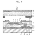
- FIG. 1 is a schematic cross-sectional view illustrating an organic light emitting display apparatus according to an embodiment of the present invention
- FIGS. 2 through 4 are schematic cross-sectional views illustrating modified versions of the organic light emitting display apparatus of FIG. 1 , according to an embodiment of the present invention.
- FIG. 5 is a schematic cross-sectional view illustrating an organic light emitting display apparatus according to another embodiment of the present invention.
- FIG. 1 is a schematic cross-sectional view illustrating an organic light emitting display apparatus according to an embodiment of the present invention.
- Organic light emitting display apparatuses are largely classified as active matrix (AM) type organic light emitting display apparatuses and passive matrix (PM) type organic light emitting display apparatuses.
- the organic light emitting display apparatus depicted in FIG. 1 is an AM type organic light emitting display apparatus, however, embodiments of the present invention are not limited thereto and can also be a PM type organic light emitting display apparatus.
- the organic light emitting display apparatus includes a substrate 10, an organic light emitting device 30, a sealing member 50, a semi-transparent film 51, a passivation film 52, a transmissive black layer 21, and a black matrix layer 22.
- the substrate 10 can be formed of a transparent glass material having SiO 2 as a main component.
- the substrate 10 is not limited thereto. That is, the substrate 10 can be formed of a transparent plastic material.
- the substrate 10 In the case of a bottom emission type organic light emitting display apparatus in which an image is displayed through the substrate 10, the substrate 10 must be formed of a transparent material.
- the substrate 10 is not necessarily formed of a transparent material.
- a buffer layer 11 is be formed on an upper surface of the substrate 10 to secure planarity of the substrate 10 and to prevent impure elements from penetrating into the organic light emitting display apparatus.
- the buffer layer 11 can be formed of at least one of SiO 2 and SiNx.
- a thin film transistor is formed on the upper surface of the substrate 10. At least one TFT is formed in each pixel and is electrically connected to the organic light emitting device 30.
- a semiconductor layer 12 having a predetermined pattern is formed on the buffer layer 11.
- the semiconductor layer 12 can be formed of an inorganic or organic semiconductor such as an amorphous silicon or poly silicon, and includes a source region, a drain region, and a channel region.
- a gate insulating film 13 is formed of SiO2 or SiNx on an upper surface of the semiconductor layer 12 and the buffer layer 11, and a gate electrode 14 is formed in a predetermined region on an upper surface of the gate insulating film 13.
- the gate electrode 14 is connected to a gate line (not shown) that applies an ON/OFF signal to the TFT.
- An interlayer insulating layer 15 is formed on the gate electrode 14, and a source electrode 16 and a drain electrode 17 are respectively connected to the source region and the drain region of the semiconductor layer 12 through contact holes.
- the TFT is protected by a passivation film 18, which can be at least one of an inorganic insulating film and an organic insulating film.
- the inorganic insulating film can be formed of SiO 2 , SiNx, SiON, Al 2 O 3 , TiO 2 , Ta 2 O 5 , HfO 2 , ZrO 2 , BST, or PZT.
- the organic insulating film can be formed of ordinary multi-purpose polymers such as polymethyl methacrylate or polystyrene, polymer derivatives having a phenol group, an acryl polymer, an imide polymer, an arylester polymer, an amide polymer, a fluoride polymer, a p-gilyrene polymer, a vinyl alcohol polymer, or a mixture of these polymers.
- the passivation film 18 can be formed as a composite stack of an inorganic insulating film and an organic insulating film.
- a first electrode 31 that functions as an anode electrode of the organic light emitting device 30 is formed on the passivation film 18, and a pixel defining layer 36 covering the first electrode 31 is formed of an insulating material. After a predetermined opening is formed in the pixel defining layer 36, an organic light emitting layer 32 of the organic light emitting device 30 is formed in a region defined by the opening. Afterwards, a second electrode 33 that functions as a cathode electrode of the organic light emitting device 30 is formed to cover the entire pixel. The polarity of the first electrode 31 and the second electrode 33 may be reversed.
- the organic light emitting device 30 displays an image by emitting light according to current flow, and includes the first electrode 31 electrically connected to the drain electrode 17 of the TFT through a contact hole, the organic light emitting layer 32, and the second electrode 33.
- the first electrode 31 can be formed in a predetermined pattern using a photolithography method.
- the pattern of the first electrode 31 can be formed in a stripe shape separated by a predetermined distance, and in an AM type organic light emitting display apparatus, the pattern of the first electrode 31 can be formed in a shape corresponding to the shape of the pixel.
- the second electrode 33 is disposed above the first electrode 31, and can be used as a cathode electrode by connecting to an external terminal (not shown).
- the second electrode 33 can be formed in a stripe shape crossing the pattern of the first electrode 31, and in the case of the AM type organic light emitting display apparatus, the second electrode 33 can be formed on the entire region where an image is displayed. The polarity of the first electrode 31 and the second electrode 33 may be reversed.
- the first electrode 31 is a transparent electrode
- the second electrode 33 can be a reflection electrode.
- the first electrode 31 is formed of a material having a high work function such as ITO, IZO, ZnO, or In 2 O 3
- the second electrode 33 can be formed of a metal having a low work function such as Ag, Mg, Al, Pt, Pd, Au, Ni, Nd, lr, Cr, Li, or Ca.
- the first electrode 31 can be a reflection electrode and the second electrode 33 can be a transparent electrode.
- the reflection electrode that functions as the first electrode 31 is formed on the reflection film using a material having a high work function such as ITO, IZO, ZnO, or ln 2 O 3 ,
- the reflection film is formed using a metal such as Ag, Mg, Al, Pt, Pd, Au, Ni, Nd, Ir, Cr, Li, Ca, or compound of these metals.
- the transparent electrode that functions as the second electrodes 33 can be formed by depositing a metal such as Ag, Mg, Al, Pt, Pd, Au, Ni, Nd, Ir, Cr, Li, Ca, or a compound of these metals having a small work function and by forming an auxiliary electrode layer or a bus electrode line using a transparent conductive material such as ITO, IZO, ZnO, or In 2 O 3 on the metal deposition.
- a metal such as Ag, Mg, Al, Pt, Pd, Au, Ni, Nd, Ir, Cr, Li, Ca
- a transparent conductive material such as ITO, IZO, ZnO, or In 2 O 3
- the first and second electrodes 31 and 33 can be formed as transparent electrodes.
- the organic light emitting layer 32 that is interposed between the first electrode 31 and the second electrode 33 emits light according to electrical driving of the first electrode 31 and the second electrode 33.
- the organic light emitting layer 32 can be formed of a low molecular weight organic material or a polymer organic material.
- a hole transport layer (HTL) and a hole injection layer (HIL) are stacked in a direction towards the first electrode 31 from the organic light emitting layer 32
- an electron transport layer (ETL) and an electron injection layer (EIL) are stacked in a direction towards the second electrode 33 from the organic light emitting layer 32.
- various other layers can be stacked if necessary.
- the low molecular weight organic material of the organic light emitting layer 32 can be of various materials including copper phthalocyanine (CuPc), N,N'-Di(naphthalene-1-yl)-N,N'-diphenyl-benzidine (NPB), and tris-8-hydroxyquinoline aluminum (Alq3).
- CuPc copper phthalocyanine
- NPB N,N'-Di(naphthalene-1-yl)-N,N'-diphenyl-benzidine
- Alq3 tris-8-hydroxyquinoline aluminum
- an HTL is formed in a direction towards the first electrode 31 from the organic light emitting layer 32.
- the polymer HTL can be formed on the first electrode 31 using poly-(2,4)-ethylene-dihydroxy thiophene (PEDOT) or polyaniline (PANI) by an inkjet printing or a spin coating method.
- PEDOT poly-(2,4)-ethylene-dihydroxy thiophene
- PANI polyaniline
- the polymer organic light emitting layer 32 can be formed of poly-phenylenevinylene (PPV), soluble PPV's, cyano-PPV, or polyfluorene and a color pattern is formed using conventional methods such as an inkjet printing method, a spin coating method, or a thermal transcribing method using a laser.
- the sealing member 50 that seals the organic light emitting device 30 is formed on the organic light emitting device 30.
- the sealing member 50 protects the organic light emitting device 30 from external moisture or oxygen.
- the sealing member 50 is formed of a transparent material.
- the top emission type organic light emitting display apparatus can be a structure in which a plurality of layers such as a glass substrate, a plastic substrate, or organic and inorganic materials are stacked.
- the semi-transparent film 51 that transmits a part of external light and reflects another part of the external light is formed on an upper surface of the sealing member 50 facing the outside.
- the semi-transparent film 51 may be formed to have reflectance of 1.5 to 5.
- the semi-transparent film 51 can be formed in a metal colloid using a metal such as Ag, Au, or Ti.
- the semi-transparent film 51 can be easily formed by an annealing process after a metal colloid film is coated by spin coating, dip coating or bar coating.
- the semi-transparent film 51 can be formed to have an optical transmittance of 40 to 80% by controlling the thickness of the semi-transparent film 51 or the process conditions when the metal colloid is formed.
- the semi-transparent film 51 can be formed to have a thickness of 10 nm to 10 ⁇ m. If the thickness of the semi-transparent film 51 is excessively thick, the optical transmittance of the semi-transparent film 51 is reduced and thus, resulting in reducing the optical efficiency of light emitted from the organic light emitting device 30. Therefore, the semi-transparent film 51 is formed to a thickness of less than 10 ⁇ m. If the thickness of the semi-transparent film 51 is excessively thin, the optical transmittance of the semi-transparent film 51 excessively increases. Thus, external light can pass through the semi-transparent film 51, and as a result, the amount of external light to be reflected by the reflection electrode increases.
- the passivation film 52 is formed on the semi-transparent film 51.
- the passivation film 52 is formed to have a refractive index that is less than that of the semi-transparent film 51.
- the passivation film 52 is formed of a thermosetting resin having high impact resistance, such as urethane acrylate or epoxy resin.
- the passivation film 52 is transparent. More specifically, the passivation film 52 can be formed by a hardening process using annealing or ultraviolet rays after coating a film by spin coating, dip coating or bar coating.
- the passivation film 52 can be formed to a thickness of 10 nm to 30 ⁇ m in some embodiments.
- the passivation film 52 is formed to a thickness of 10 nm or more to secure impact resistance in some embodiments. However, if the thickness is excessively thick, an overall thickness of the organic light emitting display apparatus increases. Therefore, in some embodiments, the passivation film 52 is formed to a thickness of 30 ⁇ m or less.
- the passivation film 52 is formed of a thermosetting resin with high impact resistance and able to protect the thin semi-transparent film 51 from external impact.
- the organic light emitting display apparatus has a structure in which the semi-transparent film 51 and the passivation film 52 are formed as an overlapping structure on the sealing member 50 and the semi-transparent film 51 has a refractive index greater than that of the passivation film 52, thereby preventing the reflection of external light at an interface of the passivation film 52. That is, the combination of the semi-transparent film 51 and the passivation film 52 can function as a conventional circular polarizer.
- the optical transmittance of the organic light emitting display apparatus can easily match the optical transmittance of a conventional circular polarizer by combining the semi-transparent film 51 having an optical transmittance of 40 to 80% and the passivation film 52 that is formed of a transparent material.
- the transmissive black layer 21 is formed between the sealing member 50 and the organic light emitting device 30. Referring to FIG. 1 , the transmissive black layer 21 is formed on a surface of the sealing member 50 facing the organic light emitting device 30.
- the transmissive black layer 21 can be formed of graphite or diamond like carbon (DLC) at a temperature of 250°C or less to prevent the transmissive black layer 21 and organic light emitting device 30 from degradation using a sputtering method or a chemical vapor deposition (CVD) method.
- DLC diamond like carbon
- the transmissive black layer 21 is a partially transmissive layer that increases contrast of the organic light emitting display apparatus.
- the transmissive black layer 21 In order to increase contrast of the organic light emitting display apparatus, the transmissive black layer 21 must have an appropriate optical transmittance.
- a low optical transmittance is advantageous for increasing contrast of the organic light emitting display apparatus.
- a low optical transmittance reduces the extraction rate of light generated from the organic light emitting device 30.
- the optical transmittances of the semi-transparent film 51 and the passivation film 52 must also be considered.
- the transmissive black layer 21 is formed to have an optical transmittance of 35 to 80%.
- the optical transmittance of the organic light emitting display apparatus according to the present embodiment can be controlled from 40 to 60% even when the transmissive black layer 21, the semi-transparent film 51, and the passivation film 52 are simultaneously used. That is, the organic light emitting display apparatus according to the present embodiment can prevent reflection of external light and can increase contrast while maintaining an optical transmittance of approximately 40%, which is the optical transmittance of a conventional circular polarizer, or higher even when the transmissive black layer 21, the semi-transparent film 51, and the passivation film 52 are simultaneously used.
- the transmissive black layer 21 can include 5 to 35% hydrogen so that the transmissive black layer 21 that is formed of graphite or DLC can have a desired optical transmittance.
- the desired optical transmittance of the organic light emitting display apparatus can be obtained by controlling the thickness of the transmissive black layer 21.
- the thickness of the transmissive black layer 21 is increased, and in order to reduce the optical transmittance of the organic light emitting display apparatus, the thickness of the transmissive black layer 21 is reduced.
- the transmissive black layer 21 having a desired optical transmittance can be obtained by forming the transmissive black layer 21 to a thickness of 5 to 70 nm.
- the transmissive black layer 21 having an appropriate thickness can be formed by considering conditions of using the semi-transparent film 51, the passivation film 52, and the organic light emitting display apparatus according to the present embodiment.
- the contrast of the organic light emitting display apparatus according to the present embodiment can further increase due to the formation of the transmissive black layer 21.
- the black matrix layer 22 can be formed on the transmissive black layer 21.
- the black matrix layer 22 is patterned to be disposed in a non-display region of the organic light emitting device 30.
- the black matrix layer 22 comprises a plurality of light absorbing portions formed in regions corresponding to non-display regions of the organic light emitting device.
- a display region of the organic light emitting device 30 is a region where the organic light emitting layer 32 is located, and the non-display region of the organic light emitting device 30 is the rest regions where the organic light emitting layer 32 is not located.
- the black matrix layer 22 can be formed of graphite or chrome having a strong dark color in order to absorb external light, however, the black matrix layer 22 can also be formed of any material that can absorb external light.
- the organic light emitting display apparatus includes the semi-transparent film 51 and the passivation film 52 having a refractive index lower than that of the semi-transparent film 51 and having a high impact resistance on the sealing member 50.
- the reflection of external light, in particular, at an interface of the substrate 10 can be reduced and an external surface of the organic light emitting display apparatus can be protected from external impact.
- the transmissive black layer 21 is formed between the organic light emitting device 30 and the sealing member 50 in order to control the optical transmittance of the organic light emitting display apparatus, thereby increasing contrast of the organic light emitting display apparatus.
- the contrast of the organic light emitting display apparatus can be further increased by forming the black matrix layer 22 in the non-display region of the organic light emitting device 30.
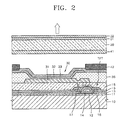
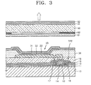
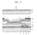
- FIGS. 2 through 4 are schematic cross-sectional views illustrating modified versions of the organic light emitting display apparatus of FIG. 1 , according to other embodiments of the present invention.
- the differences from the organic light emitting display apparatus of FIG. 1 will be mainly described.
- Like reference numerals are used to indicate elements that are substantially identical to the elements of FIG. 1 .
- the organic light emitting display apparatus includes the substrate 10, the organic light emitting device 30, the sealing member 50, the semi-transparent film 51, the passivation film 52, a transmissive black layer 41, and a black matrix layer 42.
- the transmissive black layer 41 is formed on a surface of the sealing member 50 facing the organic light emitting device 30.
- the black matrix layer 42 is formed on the second electrode 33. The rest of the structure is identical to the organic light emitting display apparatus of FIG. 1 , and thus, the detailed description thereof will not be repeated.
- the organic light emitting display apparatus includes the substrate 10, the organic light emitting device 30, the sealing member 50, the semi-transparent film 51, the passivation film 52, a transmissive black layer 61, and a black matrix layer 62.
- the black matrix layer 62 and the transmissive black layer 61 are sequentially formed on a surface of the sealing member 50 facing the organic light emitting device 30.
- the black matrix layer 62 is formed between the sealing member 50 and the transmissive black layer 61.
- the organic light emitting display apparatus includes the substrate 10, the organic light emitting device 30, the sealing member 50, the semi-transparent film 51, the passivation film 52, a transmissive black layer 71, and a black matrix layer 72.
- the transmissive black layer 71 is formed on the second electrode 33 of the organic light emitting device 30.
- the patterned black matrix layer 72 is formed on the transmissive black layer 71.
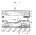
- FIG. 5 is a schematic cross-sectional view illustrating an organic light emitting display apparatus according to another embodiment of the present invention. The differences between the an organic light emitting display apparatus of FIG. 5 and the organic light emitting display apparatus of FIG. 1 will be mainly described. Like reference numerals are used to indicate elements that are substantially identical to the elements of FIG. 1 .
- the organic light emitting display apparatus includes a substrate 10, an organic light emitting device 30, a sealing member 50, a semi-transparent film 51, a passivation film 52, a pixel defining film 46, a transmissive black layer 21, and a black matrix layer 22.
- a first electrode 31 that functions as an anode electrode of the organic. light emitting device 30 is formed on a passivation film 18, and the pixel defining layer 46 covering the passivation film 18 is formed using an insulating material. After forming a predetermined opening in the pixel defining layer 46, an organic light emitting layer 32 of the organic light emitting device 30 is formed in a region defined by the opening. Afterwards, a second electrode 33 that functions as a cathode electrode of the organic light emitting device 30 is formed to cover the entire pixels. The polarity of the first electrode 31 and the second electrode 33 may be reversed.
- the pixel defining layer 46 can be formed to have a strong dark color as an insulating layer, and in this case, the reflection of external light can be minimized, thereby increasing contrast of the organic light emitting display apparatus. In other words, the pixel defining layer 46 acts as an insulating film that absorbs light.
- the organic light emitting display apparatus of FIG. 5 can also be modified as the organic light emitting display apparatus of FIG. 1 is modified as illustrated in FIGS. 2 through 4 .
- An organic light emitting display apparatus has increased contrast.
Landscapes
- Physics & Mathematics (AREA)
- Optics & Photonics (AREA)
- Electroluminescent Light Sources (AREA)
- Devices For Indicating Variable Information By Combining Individual Elements (AREA)
Applications Claiming Priority (1)
| Application Number | Priority Date | Filing Date | Title |
|---|---|---|---|
| KR1020060123371A KR100829750B1 (ko) | 2006-12-06 | 2006-12-06 | 유기 발광 표시 장치 |
Publications (3)
| Publication Number | Publication Date |
|---|---|
| EP1930968A2 true EP1930968A2 (de) | 2008-06-11 |
| EP1930968A3 EP1930968A3 (de) | 2011-06-01 |
| EP1930968B1 EP1930968B1 (de) | 2016-04-27 |
Family
ID=39266439
Family Applications (1)
| Application Number | Title | Priority Date | Filing Date |
|---|---|---|---|
| EP07254721.9A Active EP1930968B1 (de) | 2006-12-06 | 2007-12-06 | Organische lichtemittierende Vorrichtung |
Country Status (5)
| Country | Link |
|---|---|
| US (1) | US8022616B2 (de) |
| EP (1) | EP1930968B1 (de) |
| JP (1) | JP4558763B2 (de) |
| KR (1) | KR100829750B1 (de) |
| CN (1) | CN101197390B (de) |
Cited By (6)
| Publication number | Priority date | Publication date | Assignee | Title |
|---|---|---|---|---|
| EP2197061A3 (de) * | 2008-12-10 | 2010-09-01 | Samsung Mobile Display Co., Ltd. | Organische lichtemittierende Diodenanzeige |
| EP2148264A3 (de) * | 2008-07-21 | 2011-10-12 | Samsung Mobile Display Co., Ltd. | Organische lichtemittierende Anzeigevorrichtung |
| US8629842B2 (en) | 2008-07-11 | 2014-01-14 | Samsung Display Co., Ltd. | Organic light emitting display device |
| US8743078B2 (en) | 2009-08-06 | 2014-06-03 | Samsung Display Co., Ltd. | Display apparatus |
| US8928597B2 (en) | 2008-07-11 | 2015-01-06 | Samsung Display Co., Ltd. | Organic light emitting display device |
| EP3664147A1 (de) * | 2018-12-07 | 2020-06-10 | LG Display Co., Ltd. | Elektrolumineszente anzeigevorrichtung |
Families Citing this family (23)
| Publication number | Priority date | Publication date | Assignee | Title |
|---|---|---|---|---|
| JP2008234922A (ja) * | 2007-03-19 | 2008-10-02 | Seiko Epson Corp | 有機el装置、ラインヘッド、及び電子機器 |
| KR101041145B1 (ko) * | 2008-07-09 | 2011-06-13 | 삼성모바일디스플레이주식회사 | 폴리실세스퀴옥산 공중합체, 그의 제조방법, 이를 이용하는폴리실세스퀴옥산 공중합체 박막, 및 이를 이용하는유기전계발광표시장치 |
| US8058783B2 (en) * | 2008-07-25 | 2011-11-15 | Samsung Mobile Display Co., Ltd. | Organic light emitting diode display for suppressing reflection of external light |
| JP5470813B2 (ja) * | 2008-11-20 | 2014-04-16 | ソニー株式会社 | 反射板、表示装置およびその製造方法 |
| KR100989135B1 (ko) * | 2009-01-07 | 2010-10-20 | 삼성모바일디스플레이주식회사 | 유기 발광 표시 장치 |
| KR101097330B1 (ko) * | 2010-01-19 | 2011-12-23 | 삼성모바일디스플레이주식회사 | 유기 발광 디스플레이 장치 및 이를 제조 하는 방법 |
| KR101135539B1 (ko) | 2010-03-05 | 2012-04-13 | 삼성모바일디스플레이주식회사 | 유기 발광 표시 장치 |
| US8427747B2 (en) | 2010-04-22 | 2013-04-23 | 3M Innovative Properties Company | OLED light extraction films laminated onto glass substrates |
| JP6163736B2 (ja) * | 2012-07-13 | 2017-07-19 | 大日本印刷株式会社 | カラーフィルタ形成基板および有機el表示装置 |
| KR101954220B1 (ko) | 2012-09-14 | 2019-03-06 | 삼성디스플레이 주식회사 | 박막 봉지 유닛, 이를 포함하는 유기 발광 표시 장치 및 그의 제조 방법 |
| JP6314451B2 (ja) * | 2012-12-27 | 2018-04-25 | 大日本印刷株式会社 | カラーフィルタ形成基板および有機el表示装置 |
| KR102082780B1 (ko) * | 2013-01-10 | 2020-03-02 | 삼성디스플레이 주식회사 | 유기발광표시장치 및 그 제조방법 |
| JP6236793B2 (ja) * | 2013-02-08 | 2017-11-29 | 大日本印刷株式会社 | カラーフィルタ形成基板とカラーフィルタ形成基板の製造方法、および有機el表示装置 |
| KR102141558B1 (ko) * | 2013-12-24 | 2020-08-05 | 엘지디스플레이 주식회사 | 플렉서블 유기전계발광소자 및 그 제조방법 |
| KR102282997B1 (ko) | 2014-09-05 | 2021-07-29 | 삼성디스플레이 주식회사 | 유기 발광 표시장치 및 그 제조방법 |
| KR102299189B1 (ko) * | 2014-12-09 | 2021-09-08 | 엘지디스플레이 주식회사 | 유기전계발광 표시장치 및 그 제조 방법 |
| JP2017212384A (ja) * | 2016-05-27 | 2017-11-30 | ソニー株式会社 | 発光素子及び表示装置 |
| JP6685206B2 (ja) * | 2016-09-01 | 2020-04-22 | 株式会社ジャパンディスプレイ | 表示装置 |
| KR102508750B1 (ko) * | 2017-11-30 | 2023-03-13 | 삼성디스플레이 주식회사 | 발광 표시 장치 |
| CN112912948B (zh) * | 2018-12-05 | 2023-06-02 | 凸版印刷株式会社 | 黑色矩阵基板及具备黑色矩阵基板的显示装置 |
| KR102722773B1 (ko) * | 2019-07-19 | 2024-10-25 | 엘지디스플레이 주식회사 | 발광 표시 장치 |
| CN111755490B (zh) * | 2020-06-22 | 2022-07-29 | 武汉华星光电半导体显示技术有限公司 | 一种显示面板 |
| KR20230095446A (ko) * | 2021-12-22 | 2023-06-29 | 엘지디스플레이 주식회사 | 표시장치 |
Citations (4)
| Publication number | Priority date | Publication date | Assignee | Title |
|---|---|---|---|---|
| US20020030440A1 (en) | 2000-08-04 | 2002-03-14 | Shunpei Yamazaki | Semiconductor device and manufacturing method therefor |
| US20030027369A1 (en) | 2001-07-03 | 2003-02-06 | Semiconductor Energy Laboratory Co., Ltd. | Light-emitting device, method of manufacturing a light-emitting device, and electronic equipment |
| US20030146446A1 (en) | 2000-05-06 | 2003-08-07 | Semiconductor Energy Laboratory Co., Ltd. | Light-emitting device and electric apparatus |
| EP1441571A1 (de) | 2001-11-01 | 2004-07-28 | Sony Corporation | Display |
Family Cites Families (29)
| Publication number | Priority date | Publication date | Assignee | Title |
|---|---|---|---|---|
| US5173800A (en) * | 1975-12-29 | 1992-12-22 | King William J | Light control with color enhancement |
| DE2915847C2 (de) * | 1978-09-29 | 1986-01-16 | Nitto Electric Industrial Co., Ltd., Ibaraki, Osaka | Elektrooptisch aktivierbare Anzeige |
| JP3551475B2 (ja) * | 1994-06-25 | 2004-08-04 | 凸版印刷株式会社 | 薄膜型el素子 |
| JP3278611B2 (ja) | 1998-05-18 | 2002-04-30 | 日本電気株式会社 | 有機el素子の封止方法 |
| JP2000040591A (ja) | 1998-07-21 | 2000-02-08 | Sony Corp | 有機電界発光素子 |
| JP2000172198A (ja) * | 1998-12-01 | 2000-06-23 | Sanyo Electric Co Ltd | エレクトロルミネッセンス表示装置 |
| JP2000173347A (ja) * | 1998-12-02 | 2000-06-23 | Mikuni Color Ltd | 透明導電膜用組成物 |
| JP2001230072A (ja) * | 2000-02-18 | 2001-08-24 | Denso Corp | 有機el表示装置 |
| JP2002055203A (ja) * | 2000-08-11 | 2002-02-20 | Fuji Photo Film Co Ltd | 透明導電性反射防止フイルム及びそれを用いた表示装置 |
| JP2002071905A (ja) * | 2000-09-04 | 2002-03-12 | Fuji Photo Film Co Ltd | 反射防止透明導電性積層フィルム |
| JP4255643B2 (ja) * | 2001-02-21 | 2009-04-15 | 株式会社半導体エネルギー研究所 | 発光装置及びその作製方法 |
| KR100437765B1 (ko) * | 2001-06-15 | 2004-06-26 | 엘지전자 주식회사 | 고온용 기판을 이용한 박막트랜지스터 제조방법과 이를 이용한 표시장치의 제조방법 |
| KR20030010334A (ko) * | 2001-07-26 | 2003-02-05 | 석경영 | 상가 정보지를 이용한 제휴카드 판촉방법 및 시스템 |
| US7098069B2 (en) | 2002-01-24 | 2006-08-29 | Semiconductor Energy Laboratory Co., Ltd. | Light emitting device, method of preparing the same and device for fabricating the same |
| JP2003303679A (ja) * | 2002-04-09 | 2003-10-24 | Canon Inc | 有機発光素子パッケージ |
| JP2004140267A (ja) * | 2002-10-18 | 2004-05-13 | Semiconductor Energy Lab Co Ltd | 半導体装置およびその作製方法 |
| JP4526776B2 (ja) * | 2003-04-02 | 2010-08-18 | 株式会社半導体エネルギー研究所 | 発光装置及び電子機器 |
| TW591567B (en) * | 2003-06-10 | 2004-06-11 | Ritdisplay Corp | Full color display panel with mirror function |
| KR20050034126A (ko) * | 2003-10-08 | 2005-04-14 | 주식회사 엘리아테크 | 적층 보호막을 갖는 유기 이엘 소자 |
| JP2005293946A (ja) * | 2004-03-31 | 2005-10-20 | Sanyo Electric Co Ltd | 有機el表示装置 |
| TWI367686B (en) | 2004-04-07 | 2012-07-01 | Semiconductor Energy Lab | Light emitting device, electronic device, and television device |
| KR100577693B1 (ko) * | 2004-05-20 | 2006-05-10 | 광주과학기술원 | 콜로이드 다중 입자층 구조를 이용한 반사 방지막과 이의제조방법 |
| WO2006001310A1 (ja) | 2004-06-25 | 2006-01-05 | Mitsubishi Materials Corporation | 金属コロイド粒子、金属コロイド、及び金属コロイドの用途 |
| US8013809B2 (en) * | 2004-06-29 | 2011-09-06 | Semiconductor Energy Laboratory Co., Ltd. | Display device and driving method of the same, and electronic apparatus |
| JP4239983B2 (ja) | 2004-07-13 | 2009-03-18 | セイコーエプソン株式会社 | 有機el装置 |
| JP4541184B2 (ja) * | 2005-02-28 | 2010-09-08 | 株式会社クラレ | 難燃性熱可塑性重合体組成物 |
| GB0510721D0 (en) | 2005-05-25 | 2005-06-29 | Cambridge Display Tech Ltd | Electroluminescent device |
| TWI299239B (en) * | 2005-11-10 | 2008-07-21 | Au Optronics Corp | Organic light emitting display |
| US20070116934A1 (en) * | 2005-11-22 | 2007-05-24 | Miller Scott M | Antireflective surfaces, methods of manufacture thereof and articles comprising the same |
-
2006
- 2006-12-06 KR KR1020060123371A patent/KR100829750B1/ko not_active Expired - Fee Related
-
2007
- 2007-06-28 JP JP2007171084A patent/JP4558763B2/ja active Active
- 2007-12-05 US US11/951,283 patent/US8022616B2/en active Active
- 2007-12-06 CN CN2007101941619A patent/CN101197390B/zh active Active
- 2007-12-06 EP EP07254721.9A patent/EP1930968B1/de active Active
Patent Citations (4)
| Publication number | Priority date | Publication date | Assignee | Title |
|---|---|---|---|---|
| US20030146446A1 (en) | 2000-05-06 | 2003-08-07 | Semiconductor Energy Laboratory Co., Ltd. | Light-emitting device and electric apparatus |
| US20020030440A1 (en) | 2000-08-04 | 2002-03-14 | Shunpei Yamazaki | Semiconductor device and manufacturing method therefor |
| US20030027369A1 (en) | 2001-07-03 | 2003-02-06 | Semiconductor Energy Laboratory Co., Ltd. | Light-emitting device, method of manufacturing a light-emitting device, and electronic equipment |
| EP1441571A1 (de) | 2001-11-01 | 2004-07-28 | Sony Corporation | Display |
Cited By (11)
| Publication number | Priority date | Publication date | Assignee | Title |
|---|---|---|---|---|
| US8629842B2 (en) | 2008-07-11 | 2014-01-14 | Samsung Display Co., Ltd. | Organic light emitting display device |
| US8928597B2 (en) | 2008-07-11 | 2015-01-06 | Samsung Display Co., Ltd. | Organic light emitting display device |
| US9893126B2 (en) | 2008-07-11 | 2018-02-13 | Samsung Display Co., Ltd. | Organic light emitting display device |
| US10936132B2 (en) | 2008-07-11 | 2021-03-02 | Samsung Display Co., Ltd. | Organic light emitting display device |
| EP2148264A3 (de) * | 2008-07-21 | 2011-10-12 | Samsung Mobile Display Co., Ltd. | Organische lichtemittierende Anzeigevorrichtung |
| US9342176B2 (en) | 2008-07-21 | 2016-05-17 | Samsung Display Co., Ltd. | Organic light emitting display device |
| US9772709B2 (en) | 2008-07-21 | 2017-09-26 | Samsung Display Co., Ltd. | Organic light emitting display device |
| EP2197061A3 (de) * | 2008-12-10 | 2010-09-01 | Samsung Mobile Display Co., Ltd. | Organische lichtemittierende Diodenanzeige |
| US8743078B2 (en) | 2009-08-06 | 2014-06-03 | Samsung Display Co., Ltd. | Display apparatus |
| EP3664147A1 (de) * | 2018-12-07 | 2020-06-10 | LG Display Co., Ltd. | Elektrolumineszente anzeigevorrichtung |
| US11211588B2 (en) | 2018-12-07 | 2021-12-28 | Lg Display Co., Ltd. | Electroluminescent display device |
Also Published As
| Publication number | Publication date |
|---|---|
| CN101197390B (zh) | 2012-02-08 |
| US8022616B2 (en) | 2011-09-20 |
| US20080138657A1 (en) | 2008-06-12 |
| JP4558763B2 (ja) | 2010-10-06 |
| JP2008147161A (ja) | 2008-06-26 |
| CN101197390A (zh) | 2008-06-11 |
| EP1930968B1 (de) | 2016-04-27 |
| EP1930968A3 (de) | 2011-06-01 |
| KR100829750B1 (ko) | 2008-05-15 |
Similar Documents
| Publication | Publication Date | Title |
|---|---|---|
| EP1930968B1 (de) | Organische lichtemittierende Vorrichtung | |
| US8237356B2 (en) | Organic light emitting display device | |
| US7947973B2 (en) | Organic light-emitting device | |
| US8461591B2 (en) | Organic light emitting display apparatus and method of manufacturing the same | |
| US7985113B2 (en) | Retardation layer and organic light-emitting device including the same | |
| US7772768B2 (en) | Polarizer and flat panel display apparatus including the same | |
| US8998446B2 (en) | Optical film and organic light emitting display apparatus comprising the same | |
| US8952900B2 (en) | Touch screen display apparatus | |
| US8227845B2 (en) | Organic light emitting display | |
| US7868527B2 (en) | Polarizer, method of manufacturing the same, and flat panel display device including the polarizer | |
| US8188651B2 (en) | Organic light emitting display apparatus | |
| US8888547B2 (en) | Organic light-emitting display apparatus and method of manufacturing the same | |
| US7911136B2 (en) | Polarizer and organic light emitting display apparatus including the same | |
| KR100863907B1 (ko) | 유기 발광 표시 장치 |
Legal Events
| Date | Code | Title | Description |
|---|---|---|---|
| PUAI | Public reference made under article 153(3) epc to a published international application that has entered the european phase |
Free format text: ORIGINAL CODE: 0009012 |
|
| 17P | Request for examination filed |
Effective date: 20071219 |
|
| AK | Designated contracting states |
Kind code of ref document: A2 Designated state(s): AT BE BG CH CY CZ DE DK EE ES FI FR GB GR HU IE IS IT LI LT LU LV MC MT NL PL PT RO SE SI SK TR |
|
| AX | Request for extension of the european patent |
Extension state: AL BA HR MK RS |
|
| RAP1 | Party data changed (applicant data changed or rights of an application transferred) |
Owner name: SAMSUNG MOBILE DISPLAY CO., LTD. |
|
| PUAL | Search report despatched |
Free format text: ORIGINAL CODE: 0009013 |
|
| AK | Designated contracting states |
Kind code of ref document: A3 Designated state(s): AT BE BG CH CY CZ DE DK EE ES FI FR GB GR HU IE IS IT LI LT LU LV MC MT NL PL PT RO SE SI SK TR |
|
| AX | Request for extension of the european patent |
Extension state: AL BA HR MK RS |
|
| AKX | Designation fees paid |
Designated state(s): DE FR GB HU |
|
| RAP1 | Party data changed (applicant data changed or rights of an application transferred) |
Owner name: SAMSUNG DISPLAY CO., LTD. |
|
| 17Q | First examination report despatched |
Effective date: 20130626 |
|
| GRAP | Despatch of communication of intention to grant a patent |
Free format text: ORIGINAL CODE: EPIDOSNIGR1 |
|
| RAP1 | Party data changed (applicant data changed or rights of an application transferred) |
Owner name: SAMSUNG DISPLAY CO., LTD. |
|
| RIC1 | Information provided on ipc code assigned before grant |
Ipc: H01L 27/32 20060101ALI20150903BHEP Ipc: H01L 51/52 20060101AFI20150903BHEP |
|
| INTG | Intention to grant announced |
Effective date: 20151001 |
|
| GRAS | Grant fee paid |
Free format text: ORIGINAL CODE: EPIDOSNIGR3 |
|
| GRAA | (expected) grant |
Free format text: ORIGINAL CODE: 0009210 |
|
| INTG | Intention to grant announced |
Effective date: 20160307 |
|
| AK | Designated contracting states |
Kind code of ref document: B1 Designated state(s): DE FR GB HU |
|
| REG | Reference to a national code |
Ref country code: GB Ref legal event code: FG4D |
|
| REG | Reference to a national code |
Ref country code: DE Ref legal event code: R096 Ref document number: 602007046017 Country of ref document: DE |
|
| REG | Reference to a national code |
Ref country code: FR Ref legal event code: PLFP Year of fee payment: 10 |
|
| REG | Reference to a national code |
Ref country code: DE Ref legal event code: R097 Ref document number: 602007046017 Country of ref document: DE |
|
| PLBE | No opposition filed within time limit |
Free format text: ORIGINAL CODE: 0009261 |
|
| STAA | Information on the status of an ep patent application or granted ep patent |
Free format text: STATUS: NO OPPOSITION FILED WITHIN TIME LIMIT |
|
| 26N | No opposition filed |
Effective date: 20170130 |
|
| REG | Reference to a national code |
Ref country code: FR Ref legal event code: PLFP Year of fee payment: 11 |
|
| PG25 | Lapsed in a contracting state [announced via postgrant information from national office to epo] |
Ref country code: HU Free format text: LAPSE BECAUSE OF FAILURE TO SUBMIT A TRANSLATION OF THE DESCRIPTION OR TO PAY THE FEE WITHIN THE PRESCRIBED TIME-LIMIT; INVALID AB INITIO Effective date: 20071206 |
|
| REG | Reference to a national code |
Ref country code: DE Ref legal event code: R079 Ref document number: 602007046017 Country of ref document: DE Free format text: PREVIOUS MAIN CLASS: H01L0051520000 Ipc: H10K0050800000 |
|
| P01 | Opt-out of the competence of the unified patent court (upc) registered |
Effective date: 20230515 |
|
| PGFP | Annual fee paid to national office [announced via postgrant information from national office to epo] |
Ref country code: DE Payment date: 20241121 Year of fee payment: 18 |
|
| PGFP | Annual fee paid to national office [announced via postgrant information from national office to epo] |
Ref country code: GB Payment date: 20241121 Year of fee payment: 18 |
|
| PGFP | Annual fee paid to national office [announced via postgrant information from national office to epo] |
Ref country code: FR Payment date: 20241121 Year of fee payment: 18 |