EP1929486B1 - Variable integrierte induktivität - Google Patents
Variable integrierte induktivität Download PDFInfo
- Publication number
- EP1929486B1 EP1929486B1 EP06792885A EP06792885A EP1929486B1 EP 1929486 B1 EP1929486 B1 EP 1929486B1 EP 06792885 A EP06792885 A EP 06792885A EP 06792885 A EP06792885 A EP 06792885A EP 1929486 B1 EP1929486 B1 EP 1929486B1
- Authority
- EP
- European Patent Office
- Prior art keywords
- inductor
- secondary inductors
- pair
- primary inductor
- loop primary
- Prior art date
- Legal status (The legal status is an assumption and is not a legal conclusion. Google has not performed a legal analysis and makes no representation as to the accuracy of the status listed.)
- Active
Links
Images


Classifications
-
- H—ELECTRICITY
- H01—ELECTRIC ELEMENTS
- H01F—MAGNETS; INDUCTANCES; TRANSFORMERS; SELECTION OF MATERIALS FOR THEIR MAGNETIC PROPERTIES
- H01F17/00—Fixed inductances of the signal type
-
- H—ELECTRICITY
- H01—ELECTRIC ELEMENTS
- H01F—MAGNETS; INDUCTANCES; TRANSFORMERS; SELECTION OF MATERIALS FOR THEIR MAGNETIC PROPERTIES
- H01F21/00—Variable inductances or transformers of the signal type
- H01F21/12—Variable inductances or transformers of the signal type discontinuously variable, e.g. tapped
-
- H—ELECTRICITY
- H01—ELECTRIC ELEMENTS
- H01F—MAGNETS; INDUCTANCES; TRANSFORMERS; SELECTION OF MATERIALS FOR THEIR MAGNETIC PROPERTIES
- H01F17/00—Fixed inductances of the signal type
- H01F17/0006—Printed inductances
-
- H—ELECTRICITY
- H10—SEMICONDUCTOR DEVICES; ELECTRIC SOLID-STATE DEVICES NOT OTHERWISE PROVIDED FOR
- H10D—INORGANIC ELECTRIC SEMICONDUCTOR DEVICES
- H10D84/00—Integrated devices formed in or on semiconductor substrates that comprise only semiconducting layers, e.g. on Si wafers or on GaAs-on-Si wafers
-
- H—ELECTRICITY
- H01—ELECTRIC ELEMENTS
- H01F—MAGNETS; INDUCTANCES; TRANSFORMERS; SELECTION OF MATERIALS FOR THEIR MAGNETIC PROPERTIES
- H01F21/00—Variable inductances or transformers of the signal type
- H01F21/12—Variable inductances or transformers of the signal type discontinuously variable, e.g. tapped
- H01F2021/125—Printed variable inductor with taps, e.g. for VCO
-
- H—ELECTRICITY
- H01—ELECTRIC ELEMENTS
- H01L—SEMICONDUCTOR DEVICES NOT COVERED BY CLASS H10
- H01L23/00—Details of semiconductor or other solid state devices
- H01L23/52—Arrangements for conducting electric current within the device in operation from one component to another, i.e. interconnections, e.g. wires, lead frames
- H01L23/522—Arrangements for conducting electric current within the device in operation from one component to another, i.e. interconnections, e.g. wires, lead frames including external interconnections consisting of a multilayer structure of conductive and insulating layers inseparably formed on the semiconductor body
- H01L23/5227—Inductive arrangements or effects of, or between, wiring layers
-
- H—ELECTRICITY
- H01—ELECTRIC ELEMENTS
- H01L—SEMICONDUCTOR DEVICES NOT COVERED BY CLASS H10
- H01L2924/00—Indexing scheme for arrangements or methods for connecting or disconnecting semiconductor or solid-state bodies as covered by H01L24/00
- H01L2924/0001—Technical content checked by a classifier
- H01L2924/0002—Not covered by any one of groups H01L24/00, H01L24/00 and H01L2224/00
-
- Y—GENERAL TAGGING OF NEW TECHNOLOGICAL DEVELOPMENTS; GENERAL TAGGING OF CROSS-SECTIONAL TECHNOLOGIES SPANNING OVER SEVERAL SECTIONS OF THE IPC; TECHNICAL SUBJECTS COVERED BY FORMER USPC CROSS-REFERENCE ART COLLECTIONS [XRACs] AND DIGESTS
- Y10—TECHNICAL SUBJECTS COVERED BY FORMER USPC
- Y10T—TECHNICAL SUBJECTS COVERED BY FORMER US CLASSIFICATION
- Y10T29/00—Metal working
- Y10T29/49—Method of mechanical manufacture
- Y10T29/49002—Electrical device making
- Y10T29/4902—Electromagnet, transformer or inductor
Definitions
- the present invention relates to a variable integrated inductor which has an inductance value that can be switched between two or more values.
- the variable integrated inductor is used in a voltage controlled oscillator (VCO) which is of the type that can be used in a multi-band RF radio transceiver (e.g., wireless communication devices, such as mobile telephones, pagers, laptop computers, personal digital assistants (PDAs) and the like).
- VCO voltage controlled oscillator
- the variable integrated inductor can be used in a tuned amplifier load, an impedance matching network, a digitally controlled oscillator or any type of frequency selective LC-network.
- FIGURE 1 there is a block diagram that illustrates the basic components of a traditional direct conversion multi-band radio transceiver 100 (e.g., wireless communication device 100).
- the multi-band radio transceiver 100 shown includes an antenna 102, a transmit/receive (T/R) unit 104, a receive path 106, a transmit path 108 and a base-band signal processing unit 110.
- the receive path 106 includes a mixer 112 that is used together with a voltage controlled oscillator (VCO) 114 to down-convert a RF frequency signal, which is received by the antenna 102, to a lower frequency that is suitable for further signal processing in the base-band signal processing unit 110.
- VCO voltage controlled oscillator
- the transmit path 108 includes a mixer 116 that is used together with a VCO 118 to up-convert a base-band signal, which is received from the base-band signal processing unit 110, to a higher frequency before it is transmitted by the antenna 102. Since, the RF frequency (f RF ) of the received signal and the transmitted signal can vary over a very wide range (more than a factor of 2), the multi-band transceiver 100 requires that both VCOs 114 and 118 be tunable over a wide frequency range.
- the VCOs 114 and 118 have an oscillating frequency (f 0 ) which is set by a LC resonator circuit 120 that contains a fixed inductor 121 and a variable capacitor 123 which are connected in parallel.
- the tuning range of the LC resonator circuit 120 is limited to the capacitance ratio that can be achieved by adjusting the variable capacitor 123 (i.e. varicap 123 and capacitance switch 123).
- the limited tuning range of the LC-network 120 is not only a problem with multi-band radio transceivers 100. It is also a problem with other types of frequency selective LC-networks that can be, for example, used in tuned amplifier loads and impedance matching networks. A number of solutions which have been used in the past to address this problem are described next with respect to FIGURES 2-5 .
- FIGURE 2 there is a block diagram of a dual VCO 200 which has two VCOs 202a and 202b that are both connected to a multiplexer 204.
- Each VCO 202a and 202b has a LC resonator circuit 206a and 206b which contains a fixed inductor 205 and a variable capacitor 207 that are connected to one another in parallel.
- the dual VCO 200 has a total frequency range of V out that is made up of two sub-ranges of V out1 and V out2 which are outputted by VCOs 202a and 202b.
- the dual VCO 200 is relatively easy to implement, it utilizes more than twice the silicon area than is used to make the VCO 114 (for example) shown in FIGURE 1 . This is not desirable.
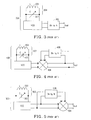
- FIGURE 3 there is a block diagram of a VCO 300 which is connected to a divider 302.
- the VCO 300 has a LC resonator circuit 304 which contains a fixed inductor 305 and a variable capacitor 307 that are connected to one another in parallel.
- the addition of the divider 302 at the output of the VCO 300 where the division ratio can be set to different integer values for different output frequency bands effectively decreases the tuning range requirements on the VCO 300.
- the addition of the divider 302 causes a significant increase of the current consumption, especially if the phase noise requirements are stringent.
- the addition of the divider 302 increases the total area used on the chip.
- the addition of the divider 302 it is often difficult to generate quadrature output signals for divider ratios that are not multiples of 2. None of these characteristics are desirable.
- FIGURE 4 there is a block diagram of a complex feed-back frequency generation scheme that has been used to implement a fractional division of the output signal of a VCO 400.
- the VCO 400 has a LC-type resonator circuit 402 which contains a fixed inductor 403 and a variable capacitor 405 that are connected to one another in parallel.
- the VCO's output signal is input into a mixer 404 which mixes that signal with a signal that passed through the mixer 404 and was divided by an integer N in a divider 406.
- the drawbacks of this scheme are that it consumes more current and takes up more space on the chip than anyone of the previous solutions shown in FIGURES 2-3 .
- FIGURE 5 there is a block diagram of a complex feed-forward frequency generation scheme that has also been used to implement a fractional division of the output signal of a VCO 500.
- the VCO 500 has a LC resonator circuit 502 which contains a fixed inductor 503 and a variable capacitor 505 that are connected to one another in parallel.
- the VCO's output signal is input into a mixer 504 and a divider 506.
- the divider 506 functions to divide the output signal by an integer N and then input the divided signal into the mixer 504.
- the mixer 504 then mixes both the original output signal and the divided output signal and outputs signal V out .
- This scheme has the same drawbacks as the feed-back scheme shown in FIGURE 4 in that it consumes more current and takes up more space on the chip than anyone of the previous solutions shown in FIGURES 2-3 .
- variable integrated inductor of the present invention is such a solution.
- the present invention includes a variable integrated inductor which has an inductance value that can be switched between two or more values.
- the variable integrated inductor includes a multi-loop primary inductor which is electromagnetically coupled to a pair of secondary inductors.
- the secondary inductors are connected to one another to form a closed circuit within which the secondary inductors have a changeable topology that can be switched between a series connection and a parallel connection in order to change an inductance value which is output by the multi-loop primary inductor.
- the variable integrated inductor is used in a voltage controlled oscillator (VCO) which is of the type that can be used in a multi-band RF radio transceiver (e.g., wireless communication device).
- VCO voltage controlled oscillator
- the variable integrated inductor can be used in a tuned amplifier load, an impedance matching network, a digitally controlled oscillator or any other type of frequency selective LC-network.
- FIGURE 6 there is a block diagram illustrating a VCO 600 that has a LC resonator circuit 602 which includes a variable integrated inductor 604 (present invention) and a variable capacitor 606.
- the variable integrated inductor 604 implements a unique inductive switching technique which is described below that enables it's inductance to be switched between two or more values.
- the VCO 600 that uses both the variable integrated inductor 604 and the variable capacitor 606 has a tuning range which can be extended by utilizing both inductive switching and capacitive switching (see Equation No. 1). In the past, this extended tuning range was not possible, because the traditional VCO 114 (for example) had a tuning range that could be changed by using only capacitive switching (via the variable capacitor 123) since the inductor 121 was fixed (see FIGURE 1 ).
- the variable integrated inductor 604 implements this unique inductive switching technique by adding a number of secondary inductors in the same chip area as a primary inductor (see FIGURES 10-13 ).
- the secondary inductors are not physically connected to the primary inductor but instead are electromagnetically coupled to the primary inductor.
- the secondary inductors themselves can be connected to one another in different configurations/topologies so one can change the influence that the secondary inductors have on the primary inductor. In particular, one can switch the configuration/topology of the secondary inductors and change a value of the total inductance that is output by the primary inductor.
- the preferred embodiment of the present invention uses two secondary inductors L 21 and L 22 that are electromagnetically coupled and not physically coupled to a primary inductor L 1 (see FIGURES 7-8 ).
- the two secondary inductors L 21 and L 22 should have identical inductances and they should have identical couplings to the primary inductor L 1 .
- the two secondary inductors L 21 and L 22 should have coupling coefficients k with opposite signs. In this way, the resulting equivalent inductance of the three electromagnetically coupled structures L 1 , L 21 and L 22 depends on how the two secondary devices L 21 and L 22 are connected to each other.
- the overall Q-factor of the variable integrated inductor 604 will also decrease due to the fact that the loss resistance is not reduced by the same amount as the inductance value.
- the two secondary inductors L 21 and L 22 are always connected to one another to form a closed circuit, it is the only topology within this closed circuit that can be changed by connecting them in series or parallel.
- the integrated inductors L 1 , L 21 and L 22 are implemented as metal traces on top of a semiconductor substrate (chip). All of the important performance parameters like the inductance value, the Q-factor, and the electromagnetic coupling to other metal structures are defined by the geometric properties of the inductor layout together with the material properties of the substrate. As such, it is important to properly size and layout the metal traces which are used to make the integrated inductors L 1 , L 21 and L 22 . A description is provided next about some different layouts which can be used to make the integrated inductors L 1 , L 21 and L 22 .
- FIGURE 9 there is illustrated a block diagram that shows a layout of a single-turn figure 8 shaped primary inductor L 1 .
- the primary inductor L 1 has the form of a single-turn figure 8 shaped structure with an upper loop 902 and a lower loop 904.
- current in the upper loop 902 travels in a direction (e.g., clockwise, see arrows) that is opposite to current in the lower loop 904 (e.g., counterclockwise, see arrows).
- the figure-8 geometry has the advantage that the magnetic fields 906 and 908 emitted from the two sub-loops 902 and 904 have opposite directions.
- FIGURE 10 there is illustrated a block diagram of an exemplary variable integrated inductor 604 that shows two secondary inductors L 21 and L 22 that are electromagnetically coupled to the single-turn figure 8 shaped primary inductor L 1 in accordance with the present invention.
- a switch 1002 in the center is left open resulting in a closed circuit series connection of the two secondary inductors L 21 and L 22 .
- the switch 1002 can be a large metal oxide semiconductor (MOS) transistor 1002 that can be controlled by software.
- MOS metal oxide semiconductor
- the symmetrical figure-8 shape of the primary inductor L 1 automatically ensures that the coupling coefficients k of the secondary inductors L 21 and L 22 have opposite signs. This is due to the fact that the primary inductor L 1 has two sub-loops 902 and 904 which have opposing magnetic fields 906 and 908. As a result, the variable integrated inductor 604 in this configuration functions like the circuit shown in FIGURE 7 and the total inductance L TOT is equal to the inductance of the primary inductor L 1 .
- FIGURE 11 there is illustrated a block diagram of the exemplary variable integrated inductor 604 shown in FIGURE 10 where the switch 1002 is closed so the secondary inductors L 21 and L 22 are connected in parallel.
- the full layout symmetry between the inductors L 1 , L 21 and L 22 guarantees that the coupling coefficients k of the second inductors L 21 and L 22 are identical in magnitude.
- the geometries of the inductors L 1 , L 21 and L 22 have not changed so the secondary inductors L 21 and L 22 still have coupling coefficients k with opposite signs.
- the variable integrated inductor 604 in this configuration functions like the circuit shown in FIGURE 8 and the total inductance L TOT is reduced in accordance with Equation No. 3.
- FIGURE 12 there is illustrated a block diagram of an exemplary variable integrated inductor 604' that has two secondary inductors L 21 and L 22 which are electromagnetically coupled to the double-turn figure 8 shaped primary inductor L 1 in accordance with another embodiment of the present invention.
- the double-turn figure 8 shaped primary inductor L 1 is very similar to the single-turn figure 8 shaped primary inductor L 1 shown in FIGURES 10-11 in that it has an upper loop 902 and a lower loop 904.
- the double-turn figure 8 shaped primary inductor L 1 that has 2 turns has a lower Q-factor and is structurally smaller for the same inductance value when compared to the single-turn figure 8 shaped primary inductor L 1 shown in FIGURES 10-11 .
- the switching mechanism 1002 can be the same as the one shown in FIGURES 10-11 .
- the use of multiple pairs of secondary inductors may be desirable since using inductive switches instead of capacitive switches for frequency tuning is probably less sensitive to differences in process parameters. This is because the inductive switches are closely linked to device geometry which can be more tightly controlled.
- the magnitude of the coupling coefficients k can be controlled by using laser-cutting tools to change the geometry (e.g., size, shape) of the secondary inductors relative to the primary inductor L 1 .
- the laser-cutting tools can also be used to replace the MOS switch 1002 if one wants to perform a once for all tuning (trimming) of the variable integrated inductor 604 during production to compensate for process variations in other components that influence the VCO frequency.
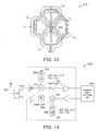
- this variable integrated inductor 604" has a cloverleaf shaped primary inductor L 1 and four secondary inductors L 21 , L 22 , L 23 and L 24 .
- the four secondary inductors L 21 , L 22 , L 23 , and L 24 are used for inductance switching where two of the secondary inductors L 21 and L 23 (for example) have positive coupling coefficients k and the other two secondary inductors L 22 and L 24 (for example) have negative coupling coefficients -k.
- the switching mechanism 1002 can be the same as the one shown in FIGURES 10-11 .
- variable integrated inductors 604, 604' and 604" can be implemented in a wide variety of devices.
- devices like tuned amplifier loads, impedance matching networks, a digitally controlled oscillator or other types of frequency selective LC-networks can benefit from incorporating and using the extended tuning range of the variable integrated inductors 604, 604' and 604".
- a multi-band radio transceiver 1400 like the one shown in FIGURE 14 can benefit from the use of two variable integrated inductors 604, 604' and 604".
- the multi-band radio transceiver 1400 (e.g., wireless communication device 1400) shown includes an antenna 1402, a transmit/receive (T/R) unit 1404, a receive path 1406, a transmit path 1408 and a base-band signal processing unit 1410.
- the receive path 1406 includes a mixer 1412 that is used together with a VCO 1414 to down-convert a RF frequency signal, which is received by the antenna 1402, to a lower frequency that is suitable for further signal processing in the base-band signal processing unit 1410.
- the transmit path 1408 includes a mixer 1416 that is used together with a
- VCO 1418 to up-convert a base-band signal, which is received from the base-band signal processing unit 1410, to a higher frequency before it is transmitted by the antenna 1402.
- the multi-band radio transceiver 1400 has the same configuration as the traditional multi-band radio transceiver 100 shown in FIGURE 1 except that the tuning ranges of the VCOs 1414 and 1418 are larger than the tuning ranges of the VCOs 114 and 118 used in the traditional multi-band radio transceiver 100.
- the VCOs 1414 and 1418 have an extended tuning range because they can use a combination of both inductive switching (via the variable integrated inductor 604, 604' and 604") and capacitive switching (via the variable capacitor 606).
- this extended tuning range was not possible because the traditional VCOs 114 and 118 had a tuning range that could be changed by using only capacitive switching (via the variable capacitor 123) since the inductor 121 was fixed (see FIGURE 1 ).
- the description provided herein about the multi-band radio transceiver 1400 omits certain details about well known components that are not necessary to understand the present invention.
- variable integrated inductors 604, 604' and 604" in the multi-band radio transceiver 1400 (or any device) is that there is less mutual EM coupling between the VCOs 1414 and 1418. This is because, each variable integrated inductor 604, 604' and 604" is symmetrical. And, since each variable integrated inductor 604, 604' and 604" consists of symmetrical multiple loops this means that each of them emit magnetic fields that tend to counteract themselves.
- variable integrated inductors 604, 604' and 604" can be placed near each other and oriented in a way such that the induced current in one variable integrated inductor 604, 604' and 604" due to the magnetic field originating from the other variable integrated inductor 604, 604' and 604" is significantly reduced.
- a multi-loop primary inductor L 1 is formed by placing metal traces on a chip.
- one or more pairs of secondary inductors L 21 and L 22 are formed by placing metal traces on the chip.
- the secondary inductors L 21 and L 22 are electromagnetically coupled to the multi-loop primary inductor L 1 .
- the secondary inductors L 21 and L 22 form a closed circuit which has a changeable topology that can be switched between a series connection and a parallel connection.
- a switch 1002 is formed on the chip. The switch 1002 is used to alter the changeable topology of the secondary inductors L 21 and L 22 and change an inductance value which is output by the multi-loop primary inductor L 1 .
Landscapes
- Engineering & Computer Science (AREA)
- Power Engineering (AREA)
- Microelectronics & Electronic Packaging (AREA)
- Inductance-Capacitance Distribution Constants And Capacitance-Resistance Oscillators (AREA)
- Coils Or Transformers For Communication (AREA)
- Networks Using Active Elements (AREA)
- Transceivers (AREA)
- Semiconductor Integrated Circuits (AREA)
- Filters And Equalizers (AREA)
- Transition And Organic Metals Composition Catalysts For Addition Polymerization (AREA)
- Inorganic Insulating Materials (AREA)
- Compositions Of Oxide Ceramics (AREA)
Claims (21)
- Variable, integrierte Induktivität (Induktor) (604), mit:einer Mehrschleifen-Primärinduktivität (L1), undeinem Paar von Sekundärinduktivitäten (L21, L22), die elektromagnetisch mit der Mehrschleifen-Primärinduktivität gekoppelt sind, wobei die Sekundärinduktivitäten miteinander verbunden sind, um eine geschlossene Schaltung zu bilden, innerhalb der die Sekundärinduktivitäten eine änderbare Topologie aufweisen, die zwischen einer Serienverbindung und einer Parallelverbindung umgeschaltet werden kann, um einen Induktanzwert zu ändern, der von der Mehrschleifen-Primärinduktivität (L1) ausgegeben wird.
- Variable, integrierte Induktivität nach Anspruch 1, wobei, wenn das Paar von Sekundärinduktivitäten (L21, L22) die Serienverbindung aufweist, es keine Änderung in dem Induktanzwert gibt, der von der Mehrschleifen-Primärinduktivität (L1) ausgegeben wird (Ltot).
- Variable, integrierte Induktivität nach Anspruch 1, wobei, wenn das Paar von Sekundärinduktivitäten (L21, L22) die Parallelverbindung aufweisen, es einen Abfall in dem Induktanzwert gibt, der von der Mehrschleifen-Primärinduktivität (L1) ausgegeben wird (Ltot).
- Variable, integrierte Induktivität nach Anspruch 1, wobei das Paar von Sekundärinduktivitäten eine Sekundärinduktivität, die eine vorbestimmte Induktanz und einen positiven Kopplungskoeffizienten (k) aufweist und eine andere Sekundärinduktivität einschließt (L21, L22), die eine vorbestimmte Induktanz und einen negativen Kopplungskoeffizienten (-k) aufweist.
- Variable, integrierte Induktivität nach Anspruch 1, wobei die Mehrschleifen-Primärinduktivität (L1) eine symmetrische Mehrschleifen-Primärinduktivität ist.
- Variable, integrierte Induktivität nach Anspruch 1, wobei die Mehrschleifen-Primärinduktivität eine 8-förmige Einzelwicklungsinduktivität ist, die zwei Unterschleifen (902, 904) aufweist, von denen die erste Unterinduktivität ein Magnetfeld in einer Richtung aufweist und die zweite Unterinduktivität ein Magnetfeld in einer entgegengesetzten Richtung aufweist.
- Variable, integrierte Induktivität nach Anspruch 1, wobei die Mehrschleifen-Primärinduktivität (L1) eine Kleeblatt-förmige Induktivität ist.
- Variable, integrierte Induktivität nach Anspruch 1, wobei die Mehrschleifen-Primärinduktivität (L1) eine 8-förmige Zweiwicklungsinduktivität ist.
- Variable, integrierte Induktivität nach Anspruch 1, weiter mit mehreren Paaren von Sekundärinduktivitäten (L21, L22, L23, L24), die verwendet werden, um eine Anzahl möglicher Induktanzwerte zu erhöhen, die von der Mehrschleifen-Primärinduktivität ausgegeben werden können.
- Variable, integrierte Induktivität nach Anspruch 1, wobei die Mehrschleifen-Primärinduktivität (L1) und das Paar von Sekundärinduktivitäten (L21, L22) in einem ausgewählten der folgenden Geräte verwendet werden:einem Spannungs-gesteuerten Oszillator (600);einer abgestimmten Verstärkerlast;einem digital-gesteuerten Oszillator;einem Impedanzanpassungsnetzwerk; undeinem Frequenz-selektiven LC-Netzwerk.
- Verfahren zum Herstellen einer geschalteten, variablen, integrierten Induktivität, wobei das Verfahren die Schritte (1500, 1502, 1504, 1506) umfasst:Bilden einer Mehrschleifen-Primärinduktivität (L1) auf einem Chip;Bilden eines Paares von Sekundärinduktivitäten (L21, L22) auf dem Chip derart, dass:das Paar von Sekundärinduktivitäten elektrisch mit der Mehrschleifen-Primärinduktivität gekoppelt ist; unddas Paar von Sekundärinduktivitäten eine geschlossene Schaltung bildet, die eine schaltbare Topologie aufweist; undBilden eines Schalters (1002) auf dem Chip, wobei der Schalter verwendet wird, die schaltbare Topologie des Paares von Sekundärinduktivitäten in entweder eine Serienverbindung oder eine Parallelverbindung zu ändern, um einen Induktanzwert zu ändern, der von der Mehrschleifen-Primärinduktivität ausgegeben wird.
- Verfahren nach Anspruch 11, wobei, wenn der Schalter (1002) sich in einer offenen Position befindet, das Paar von Sekundärinduktivitäten die Serienverbindung aufweist, die keine Änderung des Induktanzwertes verursacht, der von der Mehrschleifen-Primärinduktivität ausgegeben wird.
- Verfahren nach Anspruch 11, wobei, wenn der Schalter (1002) sich in einer geschlossenen Position verbindet, das Paar von Sekundärinduktivitäten die Parallelverbindung aufweist, die einen Abfall in dem Induktanzwert verursacht, der von der Mehrschleifen-Primärinduktivität ausgegeben wird.
- Verfahren nach Anspruch 11, wobei das Paar von Sekundärinduktivitäten (L21, L22) eine Sekundärinduktivität, die eine vorbestimmte Induktanz und einen positiven Kopplungskoeffizienten (k) aufweist und eine andere Sekundärinduktivität einschließt, die eine vorbestimmte Induktanz und einen negativen Kopplungskoeffizienten (-k) aufweist.
- Verfahren nach Anspruch 11, wobei die Mehrschleifen-Primärinduktivität (L1) eine symmetrische Mehrschleifen-Primärinduktivität ist.
- Verfahren nach Anspruch 15, wobei die Mehrschleifen-Primärinduktivität (L1) eine 8-förmige Einzelwicklungsinduktivität ist, die zwei Unterinduktivitäten (902, 904) aufweist, von denen die erste Unterinduktivität ein Magnetfeld in einer Richtung aufweist und die zweite Unterinduktivität ein Magnetfeld in einer entgegengesetzten Richtung aufweist.
- Multiband-Funktransceiver (1400), mit:einem Empfangsweg (1406), der einen ersten Spannungs-gesteuerten Oszillator (1414) einschließt, der einschließt:einen ersten variablen Kondensator; undeine erste variable, integrierte Induktivität, wobei die erste variable, integrierte Induktivität einschließt:eine erste Mehrschleifen-Primärinduktivität; undein erstes Paar von Sekundärinduktivitäten (L21, L22), die elektromagnetisch mit der ersten Mehrschleifen-Primärinduktivität gekoppelt sind, wobei das erste Paar von Sekundärinduktivitäten miteinander verbunden ist, um eine geschlossene Schaltung zu bilden, innerhalb der das erste Paar von Sekundärinduktivitäten eine änderbare Topologie aufweist, die zwischen einer Serienverbindung und einer Parallelverbindung umgeschaltet werden kann, um einen Induktanzwert zu ändern, der von der ersten Mehrschleifen-Primärinduktivität ausgegeben wird; undeinen Übertragungsweg, der einen zweiten Spannungs-gesteuerten Oszillator (1418) einschließt, der einschließt:einen zweiten variablen Kondensator; undeine zweite variable, integrierte Induktivität, wobei die zweite variable, integrierte Induktivität einschließt:eine zweite Mehrschleifen-Primärinduktivität; undein zweites Paar von Sekundärinduktivitäten, die elektromagnetisch mit der zweiten Mehrschleifen-Primärinduktivität gekoppelt sind, wobei das zweite Paar von Sekundärinduktivitäten miteinander verbunden ist, um eine geschlossene Schaltung zu bilden, innerhalb der das zweite Paar von Sekundärinduktivitäten eine änderbare Topologie aufweist, die zwischen einer Serienverbindung und einer Parallelverbindung umgeschaltet werden kann, um einen Induktanzwert zu ändern, der von der zweiten Mehrschleifen-Primärinduktivität ausgegeben wird.
- Multiband-Funktransceiver nach Anspruch 17, wobei die erste variable, integrierte Induktivität ein symmetrisches Mehrfachschleifen-Layout aufweist, das eine elektromagnetische Kopplung mit der zweiten variablen, integrierten Induktivität verringert und umgekehrt.
- Multiband-Funktransceiver nach Anspruch 17, wobei, wenn eines der Paare von Sekundärinduktivitäten die Serienverbindung aufweist, es keine Änderung in dem Induktanzwert gibt, der von der Mehrschleifen-Primärinduktivität ausgegeben wird.
- Multiband-Funktransceiver nach Anspruch 17, wobei, wenn eines der Paare von Sekundärinduktivitäten die Parallelverbindung aufweist, es einen Abfall in dem Induktanzwert gibt, der von der entsprechenden Mehrschleifen-Primärinduktivität ausgegeben wird.
- Drahtloses Kommunikationsgerät (1400), mit:einem Empfangsweg, der einen ersten Spannungs-gesteuerten Oszillator einschließt, der einschließt:einen ersten variablen Kondensator; undeine erste symmetrische, variable, integrierte Induktivität, wobei die erste, symmetrische, variable, integrierte Induktivität einschließt:eine erste Mehrschleifen-Primärinduktivität; undein erstes Paar von Sekundärinduktivitäten, die elektromagnetisch mit der ersten Mehrschleifen-Primärinduktivität gekoppelt sind, wobei das erste Paar von Sekundärinduktivitäten miteinander verbunden ist, um eine geschlossene Schaltung zu bilden, innerhalb der das erste Paar von Sekundärinduktivitäten eine änderbare Topologie aufweist, die zwischen einer Serienverbindung und einer Parallelverbindung umgeschaltet werden kann, um einen Induktanzwert zu ändern, der von der ersten Mehrschleifen-Primärinduktivität ausgegeben wird; undeinen Übertragungsweg, der einen zweiten Spannungs-gesteuerten Oszillator (1418) einschließt, der einschließt:einen zweiten variablen Kondensator; undeine zweite variable, integrierte Induktivität, wobei die zweite variable, integrierte Induktivität einschließt:eine zweite Mehrschleifen-Primärinduktivität; undein zweites Paar von Sekundärinduktivitäten, die elektromagnetisch mit der zweiten Mehrschleifen-Primärinduktivität gekoppelt sind, wobei das zweite Paar von Sekundärinduktivitäten miteinander verbunden sind, um eine geschlossene Schaltung zu bilden, innerhalb der das zweite Paar von Sekundärinduktivitäten eine änderbare Topologie aufweist, die zwischen einer Serienverbindung und einer Parallelverbindung umgeschaltet werden kann, um einen Induktanzwert zu ändern, der von der zweiten Mehrschleifen-Primärinduktivität ausgegeben wird.
Priority Applications (1)
| Application Number | Priority Date | Filing Date | Title |
|---|---|---|---|
| PL06792885T PL1929486T3 (pl) | 2005-08-29 | 2006-08-18 | Zintegrowany, zmienny element indukcyjny |
Applications Claiming Priority (2)
| Application Number | Priority Date | Filing Date | Title |
|---|---|---|---|
| US11/214,076 US7432794B2 (en) | 2004-08-16 | 2005-08-29 | Variable integrated inductor |
| PCT/EP2006/065437 WO2007025875A1 (en) | 2005-08-29 | 2006-08-18 | Variable integrated inductor |
Publications (2)
| Publication Number | Publication Date |
|---|---|
| EP1929486A1 EP1929486A1 (de) | 2008-06-11 |
| EP1929486B1 true EP1929486B1 (de) | 2009-04-29 |
Family
ID=37400885
Family Applications (1)
| Application Number | Title | Priority Date | Filing Date |
|---|---|---|---|
| EP06792885A Active EP1929486B1 (de) | 2005-08-29 | 2006-08-18 | Variable integrierte induktivität |
Country Status (14)
| Country | Link |
|---|---|
| US (1) | US7432794B2 (de) |
| EP (1) | EP1929486B1 (de) |
| JP (1) | JP5154419B2 (de) |
| KR (1) | KR101256697B1 (de) |
| CN (1) | CN101253585B (de) |
| AT (1) | ATE430371T1 (de) |
| BR (1) | BRPI0615402B1 (de) |
| CA (1) | CA2620623C (de) |
| DE (1) | DE602006006584D1 (de) |
| MY (1) | MY140388A (de) |
| PL (1) | PL1929486T3 (de) |
| RU (1) | RU2416132C2 (de) |
| TW (1) | TWI431927B (de) |
| WO (1) | WO2007025875A1 (de) |
Families Citing this family (69)
| Publication number | Priority date | Publication date | Assignee | Title |
|---|---|---|---|---|
| JP2006120735A (ja) * | 2004-10-19 | 2006-05-11 | Matsushita Electric Ind Co Ltd | インダクタ装置 |
| KR100579136B1 (ko) * | 2004-12-16 | 2006-05-12 | 한국전자통신연구원 | 가변 인덕턴스를 갖는 트랜스포머 |
| FI20055402A0 (fi) * | 2005-07-11 | 2005-07-11 | Nokia Corp | Induktorilaite monikaistaista radiotaajuista toimintaa varten |
| EP2038902B1 (de) * | 2006-07-07 | 2017-10-04 | Nxp B.V. | Programmierbarer induktor |
| DE102006035204B4 (de) * | 2006-07-29 | 2009-10-15 | Atmel Duisburg Gmbh | Monolithisch integrierbare Schaltungsanordnung |
| CN101188159B (zh) * | 2006-11-24 | 2011-01-12 | 阎跃军 | 分段可调电感器 |
| US8237531B2 (en) * | 2007-12-31 | 2012-08-07 | Globalfoundries Singapore Pte. Ltd. | Tunable high quality factor inductor |
| US8018312B2 (en) * | 2008-02-12 | 2011-09-13 | International Business Machines Corporation | Inductor and method of operating an inductor by combining primary and secondary coils with coupling structures |
| GB2462885B (en) * | 2008-08-29 | 2013-03-27 | Cambridge Silicon Radio Ltd | Inductor structure |
| EP2273613A1 (de) * | 2009-07-07 | 2011-01-12 | Nxp B.V. | Layout einer magnetischen Abschirmung, Halbleiterbauelement und Anwendung |
| EP2293309A1 (de) * | 2009-09-08 | 2011-03-09 | STmicroelectronics SA | Integrierte induktive Vorrichtung |
| KR20120088692A (ko) * | 2009-09-29 | 2012-08-08 | 텔레호낙티에볼라게트 엘엠 에릭슨(피유비엘) | 통신 네트워크에서 사용하기 위한 발진기, 주파수 합성기 및 네트워크 노드 |
| GB0918221D0 (en) * | 2009-10-16 | 2009-12-02 | Cambridge Silicon Radio Ltd | Inductor structure |
| CN103109333A (zh) | 2010-04-30 | 2013-05-15 | 鲍尔马特技术有限公司 | 在延伸区域中感应传输电能的系统和方法 |
| EP2421011A1 (de) * | 2010-08-19 | 2012-02-22 | Nxp B.V. | Symmetrischer Induktor |
| US8963674B2 (en) * | 2010-12-20 | 2015-02-24 | Mediatek Singapore Pte. Ltd. | Tunable inductor |
| US9166440B2 (en) * | 2011-01-10 | 2015-10-20 | Powermat Technologies Ltd. | System for transferring power inductively to items within a container |
| US20120244802A1 (en) * | 2011-03-24 | 2012-09-27 | Lei Feng | On chip inductor |
| US9275784B2 (en) | 2011-09-23 | 2016-03-01 | Rambus Inc. | Electronic circuits using coupled multi-inductors |
| US8576039B2 (en) * | 2011-12-06 | 2013-11-05 | Cambridge Silicon Radio Limited | Inductor structure |
| HUE025783T2 (en) * | 2012-04-03 | 2016-05-30 | ERICSSON TELEFON AB L M (publ) | An inductor layout, and a voltage-controlled oscillator (VCO) system |
| US9312820B2 (en) * | 2012-09-23 | 2016-04-12 | Dsp Group Ltd. | CMOS based TX/RX switch |
| WO2014078455A1 (en) * | 2012-11-13 | 2014-05-22 | Spectra7 Microsystems Ltd | Method and system for signal dynamic range improvement for frequency-division duplex communication systems |
| KR101351855B1 (ko) | 2012-12-03 | 2014-01-22 | 주식회사 피에스텍 | 고전력용 가변 인덕터와 이를 사용한 필터 |
| US8860521B2 (en) | 2012-12-19 | 2014-10-14 | Intel IP Corporation | Variable inductor for LC oscillator |
| US10115661B2 (en) | 2013-02-08 | 2018-10-30 | Qualcomm Incorporated | Substrate-less discrete coupled inductor structure |
| US12224096B2 (en) | 2013-03-15 | 2025-02-11 | Qorvo Us, Inc. | Advanced 3D inductor structures with confined magnetic field |
| US9705478B2 (en) | 2013-08-01 | 2017-07-11 | Qorvo Us, Inc. | Weakly coupled tunable RF receiver architecture |
| US9825656B2 (en) | 2013-08-01 | 2017-11-21 | Qorvo Us, Inc. | Weakly coupled tunable RF transmitter architecture |
| US9444417B2 (en) | 2013-03-15 | 2016-09-13 | Qorvo Us, Inc. | Weakly coupled RF network based power amplifier architecture |
| US9859863B2 (en) | 2013-03-15 | 2018-01-02 | Qorvo Us, Inc. | RF filter structure for antenna diversity and beam forming |
| US9484879B2 (en) | 2013-06-06 | 2016-11-01 | Qorvo Us, Inc. | Nonlinear capacitance linearization |
| US9774311B2 (en) | 2013-03-15 | 2017-09-26 | Qorvo Us, Inc. | Filtering characteristic adjustments of weakly coupled tunable RF filters |
| US9742359B2 (en) | 2013-03-15 | 2017-08-22 | Qorvo International Pte. Ltd. | Power amplifier with wide dynamic range am feedback linearization scheme |
| US9685928B2 (en) | 2013-08-01 | 2017-06-20 | Qorvo Us, Inc. | Interference rejection RF filters |
| US9628045B2 (en) | 2013-08-01 | 2017-04-18 | Qorvo Us, Inc. | Cooperative tunable RF filters |
| US9871499B2 (en) | 2013-03-15 | 2018-01-16 | Qorvo Us, Inc. | Multi-band impedance tuners using weakly-coupled LC resonators |
| US9755671B2 (en) | 2013-08-01 | 2017-09-05 | Qorvo Us, Inc. | VSWR detector for a tunable filter structure |
| US9780756B2 (en) | 2013-08-01 | 2017-10-03 | Qorvo Us, Inc. | Calibration for a tunable RF filter structure |
| US9899133B2 (en) | 2013-08-01 | 2018-02-20 | Qorvo Us, Inc. | Advanced 3D inductor structures with confined magnetic field |
| US9800282B2 (en) | 2013-06-06 | 2017-10-24 | Qorvo Us, Inc. | Passive voltage-gain network |
| US9705542B2 (en) | 2013-06-06 | 2017-07-11 | Qorvo Us, Inc. | Reconfigurable RF filter |
| US9780817B2 (en) | 2013-06-06 | 2017-10-03 | Qorvo Us, Inc. | RX shunt switching element-based RF front-end circuit |
| US9966981B2 (en) | 2013-06-06 | 2018-05-08 | Qorvo Us, Inc. | Passive acoustic resonator based RF receiver |
| US9172353B2 (en) | 2013-10-09 | 2015-10-27 | Analog Devices, Inc. | Programmable filter |
| EP3223309B1 (de) | 2013-10-16 | 2020-07-08 | Telefonaktiebolaget LM Ericsson (publ) | Sendeempfänger, empfänger und kommunikationsvorrichtung mit abstimmbarer induktoranordnung |
| EP3220419B1 (de) | 2013-10-16 | 2020-07-08 | Telefonaktiebolaget LM Ericsson (publ) | Sende-empfänger, empfänger und kommunikationsvorrichtung mit schalteranordnung |
| US9276616B2 (en) * | 2014-01-10 | 2016-03-01 | Qualcomm Technologies International, Ltd. | Integrated circuit chip inductor configuration |
| US9543068B2 (en) * | 2014-06-17 | 2017-01-10 | Qualcomm Technologies International, Ltd. | Inductor structure and application thereof |
| US20160125995A1 (en) * | 2014-10-31 | 2016-05-05 | Qualcomm Incorporated | Array of interleaved 8-shaped transformers with high isolation between adjacent elements |
| TWI622068B (zh) * | 2015-02-02 | 2018-04-21 | 瑞昱半導體股份有限公司 | 積體電感結構 |
| CN105990322B (zh) * | 2015-02-06 | 2019-03-15 | 瑞昱半导体股份有限公司 | 积体电感结构 |
| TWI584316B (zh) * | 2015-05-20 | 2017-05-21 | 瑞昱半導體股份有限公司 | 電感裝置 |
| US9543892B1 (en) | 2015-07-16 | 2017-01-10 | Qualcomm Incorporated | Overlapping uncoupled inductors for low-cost multi-frequency voltage-controlled oscillators |
| US10796835B2 (en) | 2015-08-24 | 2020-10-06 | Qorvo Us, Inc. | Stacked laminate inductors for high module volume utilization and performance-cost-size-processing-time tradeoff |
| US10692645B2 (en) * | 2016-03-23 | 2020-06-23 | Qorvo Us, Inc. | Coupled inductor structures |
| KR20190026828A (ko) | 2016-10-31 | 2019-03-13 | 가부시키가이샤 에구치 고오슈우하 | 리액터 |
| US11139238B2 (en) | 2016-12-07 | 2021-10-05 | Qorvo Us, Inc. | High Q factor inductor structure |
| CN108616218A (zh) * | 2016-12-13 | 2018-10-02 | 湖南格兰德芯微电子有限公司 | 射频电感变换器 |
| CN110494939B (zh) * | 2017-04-10 | 2021-07-30 | 瑞典爱立信有限公司 | 集成变压器 |
| TWI647716B (zh) * | 2017-12-26 | 2019-01-11 | 國家中山科學研究院 | Variable inductor |
| US11552594B2 (en) * | 2018-03-30 | 2023-01-10 | Intel Corporation | Oscillator frequency range extension using switched inductor |
| CN108777565B (zh) * | 2018-06-04 | 2022-08-09 | 成都仕芯半导体有限公司 | 电感耦合式谐振器及其构成的压控振荡器 |
| TWI666662B (zh) | 2018-06-20 | 2019-07-21 | 瑞昱半導體股份有限公司 | 可變電感裝置 |
| CN110660556B (zh) * | 2018-06-28 | 2021-11-12 | 瑞昱半导体股份有限公司 | 可变电感装置 |
| CN109361831A (zh) * | 2018-10-31 | 2019-02-19 | 宁波环球广电科技有限公司 | 高精度多频带电控均衡电路 |
| CN110783079B (zh) * | 2019-11-08 | 2021-11-02 | 展讯通信(上海)有限公司 | 一种电感结构 |
| US10867735B1 (en) * | 2020-03-06 | 2020-12-15 | Inphi Corporation | Inductors with compensated electromagnetic coupling |
| US11652444B2 (en) | 2021-09-20 | 2023-05-16 | Apple Inc. | Inductor topology for phase noise reduction |
Family Cites Families (25)
| Publication number | Priority date | Publication date | Assignee | Title |
|---|---|---|---|---|
| GB299731A (en) * | 1927-10-28 | 1930-01-23 | British Thomson Houston Co Ltd | Improvements relating to variable inductances |
| US4701732A (en) * | 1986-12-16 | 1987-10-20 | Hughes Aircraft Company | Fast tuning RF network inductor |
| US4816784A (en) * | 1988-01-19 | 1989-03-28 | Northern Telecom Limited | Balanced planar transformers |
| DE3912840A1 (de) * | 1989-04-19 | 1990-10-25 | Foerster Inst Dr Friedrich | Suchspulenanordnung fuer ein induktives suchgeraet |
| US5461353A (en) * | 1994-08-30 | 1995-10-24 | Motorola, Inc. | Printed circuit board inductor |
| US5585766A (en) * | 1994-10-27 | 1996-12-17 | Applied Materials, Inc. | Electrically tuned matching networks using adjustable inductance elements |
| JPH08162331A (ja) * | 1994-12-05 | 1996-06-21 | Hitachi Ltd | 可変インダクタ及びそれを用いた半導体集積回路 |
| AU3597897A (en) | 1996-07-29 | 1998-02-20 | Motorola, Inc. | Low radiation planar inductor/transformer and method |
| EP0862214A1 (de) * | 1997-02-28 | 1998-09-02 | TELEFONAKTIEBOLAGET L M ERICSSON (publ) | Integrierte Schaltung mit einer Planar-Induktivität |
| JP2771525B2 (ja) * | 1997-03-28 | 1998-07-02 | 株式会社日立製作所 | 表示装置及び表示部駆動用回路 |
| US5872489A (en) * | 1997-04-28 | 1999-02-16 | Rockwell Science Center, Llc | Integrated tunable inductance network and method |
| JP3250503B2 (ja) * | 1997-11-11 | 2002-01-28 | 株式会社村田製作所 | 可変インダクタ素子 |
| US5912596A (en) * | 1998-01-26 | 1999-06-15 | International Business Machines Corporation | Apparatus and method for frequency tuning an LC oscillator in a integrated clock circuit |
| US5952893A (en) * | 1998-03-06 | 1999-09-14 | International Business Machines Corporation | Integrated circuit inductors for use with electronic oscillators |
| US6885275B1 (en) * | 1998-11-12 | 2005-04-26 | Broadcom Corporation | Multi-track integrated spiral inductor |
| US6255913B1 (en) | 1999-10-04 | 2001-07-03 | Agere Systems Guardian Corp. | Variable frequency oscillator circuit |
| TW502264B (en) * | 2000-08-26 | 2002-09-11 | Samsung Electronics Co Ltd | RF matching unit |
| US6437653B1 (en) | 2000-09-28 | 2002-08-20 | Sun Microsystems, Inc. | Method and apparatus for providing a variable inductor on a semiconductor chip |
| US6549096B2 (en) | 2001-03-19 | 2003-04-15 | International Business Machines Corporation | Switched inductor/varactor tuning circuit having a variable integrated inductor |
| US6577219B2 (en) * | 2001-06-29 | 2003-06-10 | Koninklijke Philips Electronics N.V. | Multiple-interleaved integrated circuit transformer |
| JP2003124743A (ja) * | 2001-10-16 | 2003-04-25 | Oki Electric Ind Co Ltd | 電圧制御発振回路 |
| US6842101B2 (en) * | 2002-01-08 | 2005-01-11 | Eagle Comtronics, Inc. | Tunable inductor |
| DE10233980A1 (de) | 2002-07-25 | 2004-02-12 | Philips Intellectual Property & Standards Gmbh | Planarinduktivität |
| JP2005085701A (ja) * | 2003-09-10 | 2005-03-31 | Matsushita Electric Ind Co Ltd | 偏向ヨーク及び陰極線管装置 |
| US7460001B2 (en) * | 2003-09-25 | 2008-12-02 | Qualcomm Incorporated | Variable inductor for integrated circuit and printed circuit board |
-
2005
- 2005-08-29 US US11/214,076 patent/US7432794B2/en active Active
-
2006
- 2006-07-28 TW TW095127614A patent/TWI431927B/zh active
- 2006-08-02 MY MYPI20063744A patent/MY140388A/en unknown
- 2006-08-18 BR BRPI0615402-6A patent/BRPI0615402B1/pt active IP Right Grant
- 2006-08-18 CN CN2006800319928A patent/CN101253585B/zh active Active
- 2006-08-18 JP JP2008528460A patent/JP5154419B2/ja active Active
- 2006-08-18 DE DE602006006584T patent/DE602006006584D1/de active Active
- 2006-08-18 KR KR1020087005141A patent/KR101256697B1/ko active Active
- 2006-08-18 AT AT06792885T patent/ATE430371T1/de not_active IP Right Cessation
- 2006-08-18 PL PL06792885T patent/PL1929486T3/pl unknown
- 2006-08-18 RU RU2008112129/07A patent/RU2416132C2/ru active
- 2006-08-18 EP EP06792885A patent/EP1929486B1/de active Active
- 2006-08-18 CA CA2620623A patent/CA2620623C/en active Active
- 2006-08-18 WO PCT/EP2006/065437 patent/WO2007025875A1/en not_active Ceased
Also Published As
| Publication number | Publication date |
|---|---|
| CA2620623C (en) | 2015-02-17 |
| CA2620623A1 (en) | 2007-03-08 |
| RU2416132C2 (ru) | 2011-04-10 |
| TWI431927B (zh) | 2014-03-21 |
| DE602006006584D1 (de) | 2009-06-10 |
| JP5154419B2 (ja) | 2013-02-27 |
| BRPI0615402B1 (pt) | 2018-05-29 |
| BRPI0615402A2 (pt) | 2012-12-04 |
| CN101253585B (zh) | 2011-01-19 |
| US7432794B2 (en) | 2008-10-07 |
| KR20080039464A (ko) | 2008-05-07 |
| US20060033602A1 (en) | 2006-02-16 |
| MY140388A (en) | 2009-12-31 |
| KR101256697B1 (ko) | 2013-04-19 |
| HK1120654A1 (en) | 2009-04-03 |
| RU2008112129A (ru) | 2009-10-10 |
| JP2009506562A (ja) | 2009-02-12 |
| EP1929486A1 (de) | 2008-06-11 |
| ATE430371T1 (de) | 2009-05-15 |
| WO2007025875A1 (en) | 2007-03-08 |
| PL1929486T3 (pl) | 2009-09-30 |
| TW200713794A (en) | 2007-04-01 |
| CN101253585A (zh) | 2008-08-27 |
Similar Documents
| Publication | Publication Date | Title |
|---|---|---|
| EP1929486B1 (de) | Variable integrierte induktivität | |
| US8125282B2 (en) | Dual-band coupled VCO | |
| Zou et al. | A low phase noise and wide tuning range millimeter-wave VCO using switchable coupled VCO-cores | |
| US11336229B2 (en) | Radio frequency oscillator | |
| US9312807B2 (en) | Low phase noise voltage controlled oscillators | |
| US7154349B2 (en) | Coupled-inductor multi-band VCO | |
| EP2769466B1 (de) | Spannungsgesteuerte oszillatoren mit niedrigem phasenrauschen | |
| EP2707946B1 (de) | Rauscharmer oszillator | |
| WO2002080349A1 (en) | Oscillator with improved magnetic coupling rejection | |
| WO2019218371A1 (zh) | 一种振荡器的集成电路 | |
| JP2012253561A (ja) | 電圧制御発振器 | |
| HK1120654B (en) | Variable integrated inductor | |
| US11973465B2 (en) | Oscillator circuit |
Legal Events
| Date | Code | Title | Description |
|---|---|---|---|
| PUAI | Public reference made under article 153(3) epc to a published international application that has entered the european phase |
Free format text: ORIGINAL CODE: 0009012 |
|
| 17P | Request for examination filed |
Effective date: 20080226 |
|
| AK | Designated contracting states |
Kind code of ref document: A1 Designated state(s): AT BE BG CH CY CZ DE DK EE ES FI FR GB GR HU IE IS IT LI LT LU LV MC NL PL PT RO SE SI SK TR |
|
| GRAP | Despatch of communication of intention to grant a patent |
Free format text: ORIGINAL CODE: EPIDOSNIGR1 |
|
| GRAS | Grant fee paid |
Free format text: ORIGINAL CODE: EPIDOSNIGR3 |
|
| GRAA | (expected) grant |
Free format text: ORIGINAL CODE: 0009210 |
|
| AK | Designated contracting states |
Kind code of ref document: B1 Designated state(s): AT BE BG CH CY CZ DE DK EE ES FI FR GB GR HU IE IS IT LI LT LU LV MC NL PL PT RO SE SI SK TR |
|
| REG | Reference to a national code |
Ref country code: GB Ref legal event code: FG4D |
|
| REG | Reference to a national code |
Ref country code: CH Ref legal event code: EP |
|
| REF | Corresponds to: |
Ref document number: 602006006584 Country of ref document: DE Date of ref document: 20090610 Kind code of ref document: P |
|
| REG | Reference to a national code |
Ref country code: IE Ref legal event code: FG4D |
|
| REG | Reference to a national code |
Ref country code: PL Ref legal event code: T3 |
|
| NLV1 | Nl: lapsed or annulled due to failure to fulfill the requirements of art. 29p and 29m of the patents act | ||
| PG25 | Lapsed in a contracting state [announced via postgrant information from national office to epo] |
Ref country code: ES Free format text: LAPSE BECAUSE OF FAILURE TO SUBMIT A TRANSLATION OF THE DESCRIPTION OR TO PAY THE FEE WITHIN THE PRESCRIBED TIME-LIMIT Effective date: 20090809 Ref country code: AT Free format text: LAPSE BECAUSE OF FAILURE TO SUBMIT A TRANSLATION OF THE DESCRIPTION OR TO PAY THE FEE WITHIN THE PRESCRIBED TIME-LIMIT Effective date: 20090429 Ref country code: LT Free format text: LAPSE BECAUSE OF FAILURE TO SUBMIT A TRANSLATION OF THE DESCRIPTION OR TO PAY THE FEE WITHIN THE PRESCRIBED TIME-LIMIT Effective date: 20090429 Ref country code: FI Free format text: LAPSE BECAUSE OF FAILURE TO SUBMIT A TRANSLATION OF THE DESCRIPTION OR TO PAY THE FEE WITHIN THE PRESCRIBED TIME-LIMIT Effective date: 20090429 Ref country code: PT Free format text: LAPSE BECAUSE OF FAILURE TO SUBMIT A TRANSLATION OF THE DESCRIPTION OR TO PAY THE FEE WITHIN THE PRESCRIBED TIME-LIMIT Effective date: 20090829 |
|
| PG25 | Lapsed in a contracting state [announced via postgrant information from national office to epo] |
Ref country code: SE Free format text: LAPSE BECAUSE OF FAILURE TO SUBMIT A TRANSLATION OF THE DESCRIPTION OR TO PAY THE FEE WITHIN THE PRESCRIBED TIME-LIMIT Effective date: 20090729 Ref country code: NL Free format text: LAPSE BECAUSE OF FAILURE TO SUBMIT A TRANSLATION OF THE DESCRIPTION OR TO PAY THE FEE WITHIN THE PRESCRIBED TIME-LIMIT Effective date: 20090429 Ref country code: SI Free format text: LAPSE BECAUSE OF FAILURE TO SUBMIT A TRANSLATION OF THE DESCRIPTION OR TO PAY THE FEE WITHIN THE PRESCRIBED TIME-LIMIT Effective date: 20090429 Ref country code: LV Free format text: LAPSE BECAUSE OF FAILURE TO SUBMIT A TRANSLATION OF THE DESCRIPTION OR TO PAY THE FEE WITHIN THE PRESCRIBED TIME-LIMIT Effective date: 20090429 Ref country code: IS Free format text: LAPSE BECAUSE OF FAILURE TO SUBMIT A TRANSLATION OF THE DESCRIPTION OR TO PAY THE FEE WITHIN THE PRESCRIBED TIME-LIMIT Effective date: 20090829 |
|
| PG25 | Lapsed in a contracting state [announced via postgrant information from national office to epo] |
Ref country code: DK Free format text: LAPSE BECAUSE OF FAILURE TO SUBMIT A TRANSLATION OF THE DESCRIPTION OR TO PAY THE FEE WITHIN THE PRESCRIBED TIME-LIMIT Effective date: 20090429 Ref country code: EE Free format text: LAPSE BECAUSE OF FAILURE TO SUBMIT A TRANSLATION OF THE DESCRIPTION OR TO PAY THE FEE WITHIN THE PRESCRIBED TIME-LIMIT Effective date: 20090429 Ref country code: RO Free format text: LAPSE BECAUSE OF FAILURE TO SUBMIT A TRANSLATION OF THE DESCRIPTION OR TO PAY THE FEE WITHIN THE PRESCRIBED TIME-LIMIT Effective date: 20090429 Ref country code: CZ Free format text: LAPSE BECAUSE OF FAILURE TO SUBMIT A TRANSLATION OF THE DESCRIPTION OR TO PAY THE FEE WITHIN THE PRESCRIBED TIME-LIMIT Effective date: 20090429 |
|
| PG25 | Lapsed in a contracting state [announced via postgrant information from national office to epo] |
Ref country code: BE Free format text: LAPSE BECAUSE OF FAILURE TO SUBMIT A TRANSLATION OF THE DESCRIPTION OR TO PAY THE FEE WITHIN THE PRESCRIBED TIME-LIMIT Effective date: 20090429 Ref country code: SK Free format text: LAPSE BECAUSE OF FAILURE TO SUBMIT A TRANSLATION OF THE DESCRIPTION OR TO PAY THE FEE WITHIN THE PRESCRIBED TIME-LIMIT Effective date: 20090429 |
|
| PLBE | No opposition filed within time limit |
Free format text: ORIGINAL CODE: 0009261 |
|
| STAA | Information on the status of an ep patent application or granted ep patent |
Free format text: STATUS: NO OPPOSITION FILED WITHIN TIME LIMIT |
|
| PG25 | Lapsed in a contracting state [announced via postgrant information from national office to epo] |
Ref country code: BG Free format text: LAPSE BECAUSE OF FAILURE TO SUBMIT A TRANSLATION OF THE DESCRIPTION OR TO PAY THE FEE WITHIN THE PRESCRIBED TIME-LIMIT Effective date: 20090729 Ref country code: MC Free format text: LAPSE BECAUSE OF NON-PAYMENT OF DUE FEES Effective date: 20090831 |
|
| 26N | No opposition filed |
Effective date: 20100201 |
|
| PG25 | Lapsed in a contracting state [announced via postgrant information from national office to epo] |
Ref country code: IE Free format text: LAPSE BECAUSE OF NON-PAYMENT OF DUE FEES Effective date: 20090818 |
|
| PG25 | Lapsed in a contracting state [announced via postgrant information from national office to epo] |
Ref country code: GR Free format text: LAPSE BECAUSE OF FAILURE TO SUBMIT A TRANSLATION OF THE DESCRIPTION OR TO PAY THE FEE WITHIN THE PRESCRIBED TIME-LIMIT Effective date: 20090730 |
|
| PG25 | Lapsed in a contracting state [announced via postgrant information from national office to epo] |
Ref country code: IT Free format text: LAPSE BECAUSE OF FAILURE TO SUBMIT A TRANSLATION OF THE DESCRIPTION OR TO PAY THE FEE WITHIN THE PRESCRIBED TIME-LIMIT Effective date: 20090429 |
|
| REG | Reference to a national code |
Ref country code: CH Ref legal event code: PL |
|
| PG25 | Lapsed in a contracting state [announced via postgrant information from national office to epo] |
Ref country code: LI Free format text: LAPSE BECAUSE OF NON-PAYMENT OF DUE FEES Effective date: 20100831 Ref country code: LU Free format text: LAPSE BECAUSE OF NON-PAYMENT OF DUE FEES Effective date: 20090818 Ref country code: CH Free format text: LAPSE BECAUSE OF NON-PAYMENT OF DUE FEES Effective date: 20100831 |
|
| PG25 | Lapsed in a contracting state [announced via postgrant information from national office to epo] |
Ref country code: HU Free format text: LAPSE BECAUSE OF FAILURE TO SUBMIT A TRANSLATION OF THE DESCRIPTION OR TO PAY THE FEE WITHIN THE PRESCRIBED TIME-LIMIT Effective date: 20091030 |
|
| PG25 | Lapsed in a contracting state [announced via postgrant information from national office to epo] |
Ref country code: TR Free format text: LAPSE BECAUSE OF FAILURE TO SUBMIT A TRANSLATION OF THE DESCRIPTION OR TO PAY THE FEE WITHIN THE PRESCRIBED TIME-LIMIT Effective date: 20090429 |
|
| PG25 | Lapsed in a contracting state [announced via postgrant information from national office to epo] |
Ref country code: CY Free format text: LAPSE BECAUSE OF FAILURE TO SUBMIT A TRANSLATION OF THE DESCRIPTION OR TO PAY THE FEE WITHIN THE PRESCRIBED TIME-LIMIT Effective date: 20090429 |
|
| REG | Reference to a national code |
Ref country code: FR Ref legal event code: PLFP Year of fee payment: 11 |
|
| REG | Reference to a national code |
Ref country code: FR Ref legal event code: PLFP Year of fee payment: 12 |
|
| REG | Reference to a national code |
Ref country code: FR Ref legal event code: PLFP Year of fee payment: 13 |
|
| P01 | Opt-out of the competence of the unified patent court (upc) registered |
Effective date: 20230523 |
|
| PGFP | Annual fee paid to national office [announced via postgrant information from national office to epo] |
Ref country code: DE Payment date: 20250827 Year of fee payment: 20 |
|
| PGFP | Annual fee paid to national office [announced via postgrant information from national office to epo] |
Ref country code: PL Payment date: 20250806 Year of fee payment: 20 |
|
| PGFP | Annual fee paid to national office [announced via postgrant information from national office to epo] |
Ref country code: GB Payment date: 20250827 Year of fee payment: 20 |
|
| PGFP | Annual fee paid to national office [announced via postgrant information from national office to epo] |
Ref country code: FR Payment date: 20250825 Year of fee payment: 20 |