EP1921667A2 - Procédé de fabrication d'un dispositif semi-conducteur - Google Patents
Procédé de fabrication d'un dispositif semi-conducteur Download PDFInfo
- Publication number
- EP1921667A2 EP1921667A2 EP07021213A EP07021213A EP1921667A2 EP 1921667 A2 EP1921667 A2 EP 1921667A2 EP 07021213 A EP07021213 A EP 07021213A EP 07021213 A EP07021213 A EP 07021213A EP 1921667 A2 EP1921667 A2 EP 1921667A2
- Authority
- EP
- European Patent Office
- Prior art keywords
- film
- equal
- glass substrate
- laser beam
- semiconductor film
- Prior art date
- Legal status (The legal status is an assumption and is not a legal conclusion. Google has not performed a legal analysis and makes no representation as to the accuracy of the status listed.)
- Granted
Links
Images


Classifications
-
- H—ELECTRICITY
- H01—ELECTRIC ELEMENTS
- H01L—SEMICONDUCTOR DEVICES NOT COVERED BY CLASS H10
- H01L21/00—Processes or apparatus adapted for the manufacture or treatment of semiconductor or solid state devices or of parts thereof
- H01L21/02—Manufacture or treatment of semiconductor devices or of parts thereof
- H01L21/02104—Forming layers
- H01L21/02365—Forming inorganic semiconducting materials on a substrate
- H01L21/02656—Special treatments
- H01L21/02664—Aftertreatments
- H01L21/02667—Crystallisation or recrystallisation of non-monocrystalline semiconductor materials, e.g. regrowth
- H01L21/02675—Crystallisation or recrystallisation of non-monocrystalline semiconductor materials, e.g. regrowth using laser beams
- H01L21/02678—Beam shaping, e.g. using a mask
-
- B—PERFORMING OPERATIONS; TRANSPORTING
- B23—MACHINE TOOLS; METAL-WORKING NOT OTHERWISE PROVIDED FOR
- B23K—SOLDERING OR UNSOLDERING; WELDING; CLADDING OR PLATING BY SOLDERING OR WELDING; CUTTING BY APPLYING HEAT LOCALLY, e.g. FLAME CUTTING; WORKING BY LASER BEAM
- B23K26/00—Working by laser beam, e.g. welding, cutting or boring
- B23K26/02—Positioning or observing the workpiece, e.g. with respect to the point of impact; Aligning, aiming or focusing the laser beam
- B23K26/06—Shaping the laser beam, e.g. by masks or multi-focusing
- B23K26/073—Shaping the laser spot
- B23K26/0732—Shaping the laser spot into a rectangular shape
-
- B—PERFORMING OPERATIONS; TRANSPORTING
- B23—MACHINE TOOLS; METAL-WORKING NOT OTHERWISE PROVIDED FOR
- B23K—SOLDERING OR UNSOLDERING; WELDING; CLADDING OR PLATING BY SOLDERING OR WELDING; CUTTING BY APPLYING HEAT LOCALLY, e.g. FLAME CUTTING; WORKING BY LASER BEAM
- B23K26/00—Working by laser beam, e.g. welding, cutting or boring
- B23K26/02—Positioning or observing the workpiece, e.g. with respect to the point of impact; Aligning, aiming or focusing the laser beam
- B23K26/06—Shaping the laser beam, e.g. by masks or multi-focusing
- B23K26/073—Shaping the laser spot
- B23K26/0738—Shaping the laser spot into a linear shape
-
- H—ELECTRICITY
- H01—ELECTRIC ELEMENTS
- H01L—SEMICONDUCTOR DEVICES NOT COVERED BY CLASS H10
- H01L21/00—Processes or apparatus adapted for the manufacture or treatment of semiconductor or solid state devices or of parts thereof
- H01L21/02—Manufacture or treatment of semiconductor devices or of parts thereof
- H01L21/02104—Forming layers
- H01L21/02365—Forming inorganic semiconducting materials on a substrate
- H01L21/02367—Substrates
- H01L21/0237—Materials
- H01L21/02422—Non-crystalline insulating materials, e.g. glass, polymers
-
- H—ELECTRICITY
- H01—ELECTRIC ELEMENTS
- H01L—SEMICONDUCTOR DEVICES NOT COVERED BY CLASS H10
- H01L21/00—Processes or apparatus adapted for the manufacture or treatment of semiconductor or solid state devices or of parts thereof
- H01L21/02—Manufacture or treatment of semiconductor devices or of parts thereof
- H01L21/02104—Forming layers
- H01L21/02365—Forming inorganic semiconducting materials on a substrate
- H01L21/02518—Deposited layers
- H01L21/02521—Materials
- H01L21/02524—Group 14 semiconducting materials
- H01L21/02532—Silicon, silicon germanium, germanium
-
- H—ELECTRICITY
- H01—ELECTRIC ELEMENTS
- H01L—SEMICONDUCTOR DEVICES NOT COVERED BY CLASS H10
- H01L21/00—Processes or apparatus adapted for the manufacture or treatment of semiconductor or solid state devices or of parts thereof
- H01L21/02—Manufacture or treatment of semiconductor devices or of parts thereof
- H01L21/02104—Forming layers
- H01L21/02365—Forming inorganic semiconducting materials on a substrate
- H01L21/02656—Special treatments
- H01L21/02664—Aftertreatments
- H01L21/02667—Crystallisation or recrystallisation of non-monocrystalline semiconductor materials, e.g. regrowth
- H01L21/02675—Crystallisation or recrystallisation of non-monocrystalline semiconductor materials, e.g. regrowth using laser beams
- H01L21/02686—Pulsed laser beam
-
- H—ELECTRICITY
- H01—ELECTRIC ELEMENTS
- H01L—SEMICONDUCTOR DEVICES NOT COVERED BY CLASS H10
- H01L21/00—Processes or apparatus adapted for the manufacture or treatment of semiconductor or solid state devices or of parts thereof
- H01L21/02—Manufacture or treatment of semiconductor devices or of parts thereof
- H01L21/04—Manufacture or treatment of semiconductor devices or of parts thereof the devices having at least one potential-jump barrier or surface barrier, e.g. PN junction, depletion layer or carrier concentration layer
- H01L21/18—Manufacture or treatment of semiconductor devices or of parts thereof the devices having at least one potential-jump barrier or surface barrier, e.g. PN junction, depletion layer or carrier concentration layer the devices having semiconductor bodies comprising elements of Group IV of the Periodic System or AIIIBV compounds with or without impurities, e.g. doping materials
- H01L21/20—Deposition of semiconductor materials on a substrate, e.g. epitaxial growth solid phase epitaxy
-
- H—ELECTRICITY
- H01—ELECTRIC ELEMENTS
- H01L—SEMICONDUCTOR DEVICES NOT COVERED BY CLASS H10
- H01L21/00—Processes or apparatus adapted for the manufacture or treatment of semiconductor or solid state devices or of parts thereof
- H01L21/02—Manufacture or treatment of semiconductor devices or of parts thereof
- H01L21/04—Manufacture or treatment of semiconductor devices or of parts thereof the devices having at least one potential-jump barrier or surface barrier, e.g. PN junction, depletion layer or carrier concentration layer
- H01L21/18—Manufacture or treatment of semiconductor devices or of parts thereof the devices having at least one potential-jump barrier or surface barrier, e.g. PN junction, depletion layer or carrier concentration layer the devices having semiconductor bodies comprising elements of Group IV of the Periodic System or AIIIBV compounds with or without impurities, e.g. doping materials
- H01L21/26—Bombardment with radiation
- H01L21/263—Bombardment with radiation with high-energy radiation
- H01L21/268—Bombardment with radiation with high-energy radiation using electromagnetic radiation, e.g. laser radiation
-
- H—ELECTRICITY
- H01—ELECTRIC ELEMENTS
- H01L—SEMICONDUCTOR DEVICES NOT COVERED BY CLASS H10
- H01L21/00—Processes or apparatus adapted for the manufacture or treatment of semiconductor or solid state devices or of parts thereof
- H01L21/02—Manufacture or treatment of semiconductor devices or of parts thereof
- H01L21/04—Manufacture or treatment of semiconductor devices or of parts thereof the devices having at least one potential-jump barrier or surface barrier, e.g. PN junction, depletion layer or carrier concentration layer
- H01L21/18—Manufacture or treatment of semiconductor devices or of parts thereof the devices having at least one potential-jump barrier or surface barrier, e.g. PN junction, depletion layer or carrier concentration layer the devices having semiconductor bodies comprising elements of Group IV of the Periodic System or AIIIBV compounds with or without impurities, e.g. doping materials
- H01L21/30—Treatment of semiconductor bodies using processes or apparatus not provided for in groups H01L21/20 - H01L21/26
- H01L21/324—Thermal treatment for modifying the properties of semiconductor bodies, e.g. annealing, sintering
-
- H—ELECTRICITY
- H01—ELECTRIC ELEMENTS
- H01L—SEMICONDUCTOR DEVICES NOT COVERED BY CLASS H10
- H01L27/00—Devices consisting of a plurality of semiconductor or other solid-state components formed in or on a common substrate
- H01L27/02—Devices consisting of a plurality of semiconductor or other solid-state components formed in or on a common substrate including semiconductor components specially adapted for rectifying, oscillating, amplifying or switching and having at least one potential-jump barrier or surface barrier; including integrated passive circuit elements with at least one potential-jump barrier or surface barrier
- H01L27/12—Devices consisting of a plurality of semiconductor or other solid-state components formed in or on a common substrate including semiconductor components specially adapted for rectifying, oscillating, amplifying or switching and having at least one potential-jump barrier or surface barrier; including integrated passive circuit elements with at least one potential-jump barrier or surface barrier the substrate being other than a semiconductor body, e.g. an insulating body
- H01L27/1214—Devices consisting of a plurality of semiconductor or other solid-state components formed in or on a common substrate including semiconductor components specially adapted for rectifying, oscillating, amplifying or switching and having at least one potential-jump barrier or surface barrier; including integrated passive circuit elements with at least one potential-jump barrier or surface barrier the substrate being other than a semiconductor body, e.g. an insulating body comprising a plurality of TFTs formed on a non-semiconducting substrate, e.g. driving circuits for AMLCDs
- H01L27/1218—Devices consisting of a plurality of semiconductor or other solid-state components formed in or on a common substrate including semiconductor components specially adapted for rectifying, oscillating, amplifying or switching and having at least one potential-jump barrier or surface barrier; including integrated passive circuit elements with at least one potential-jump barrier or surface barrier the substrate being other than a semiconductor body, e.g. an insulating body comprising a plurality of TFTs formed on a non-semiconducting substrate, e.g. driving circuits for AMLCDs with a particular composition or structure of the substrate
-
- H—ELECTRICITY
- H01—ELECTRIC ELEMENTS
- H01L—SEMICONDUCTOR DEVICES NOT COVERED BY CLASS H10
- H01L27/00—Devices consisting of a plurality of semiconductor or other solid-state components formed in or on a common substrate
- H01L27/02—Devices consisting of a plurality of semiconductor or other solid-state components formed in or on a common substrate including semiconductor components specially adapted for rectifying, oscillating, amplifying or switching and having at least one potential-jump barrier or surface barrier; including integrated passive circuit elements with at least one potential-jump barrier or surface barrier
- H01L27/12—Devices consisting of a plurality of semiconductor or other solid-state components formed in or on a common substrate including semiconductor components specially adapted for rectifying, oscillating, amplifying or switching and having at least one potential-jump barrier or surface barrier; including integrated passive circuit elements with at least one potential-jump barrier or surface barrier the substrate being other than a semiconductor body, e.g. an insulating body
- H01L27/1214—Devices consisting of a plurality of semiconductor or other solid-state components formed in or on a common substrate including semiconductor components specially adapted for rectifying, oscillating, amplifying or switching and having at least one potential-jump barrier or surface barrier; including integrated passive circuit elements with at least one potential-jump barrier or surface barrier the substrate being other than a semiconductor body, e.g. an insulating body comprising a plurality of TFTs formed on a non-semiconducting substrate, e.g. driving circuits for AMLCDs
- H01L27/1259—Multistep manufacturing methods
- H01L27/127—Multistep manufacturing methods with a particular formation, treatment or patterning of the active layer specially adapted to the circuit arrangement
- H01L27/1274—Multistep manufacturing methods with a particular formation, treatment or patterning of the active layer specially adapted to the circuit arrangement using crystallisation of amorphous semiconductor or recrystallisation of crystalline semiconductor
- H01L27/1285—Multistep manufacturing methods with a particular formation, treatment or patterning of the active layer specially adapted to the circuit arrangement using crystallisation of amorphous semiconductor or recrystallisation of crystalline semiconductor using control of the annealing or irradiation parameters, e.g. using different scanning direction or intensity for different transistors
Definitions
- One aspect of the present invention is a method for manufacturing a crystalline silicon film and a semiconductor device using the crystalline silicon film, in which a semiconductor film is irradiated with a laser beam so as to be completely melted and crystals grow in a direction horizontal to a glass substrate or the semiconductor film surface.
- a layer including a semiconductor film is formed over a glass substrate having a thermal expansion coefficient of greater than 6 ⁇ 10 -7 /°C and less than or equal to 38 ⁇ 10 -7 /°C, preferably greater than 6 ⁇ 10 -7 /°C and less than or equal to 31.8 ⁇ 10 -7 /°C, and is heated.
- the layer formed over the glass substrate which has a thermal expansion coefficient of greater than 6 ⁇ 10 -7 /°C and less than or equal to 38 ⁇ 10 -7 /°C, preferably greater than 6 ⁇ 10 -7 /°C and less than or equal to 31.8 ⁇ 10 -7 /°C, is irradiated with a pulsed ultraviolet laser beam having a width of less than or equal to 100 ⁇ m, a ratio of width to length of 1:500 or more, and a full width at half maximum of the laser beam profile of less than or equal to 50 ⁇ m, energy of the laser beam with which the layer is irradiated is transmitted from the semiconductor layer to the glass substrate surface, and an irradiation part of the laser beam and also the glass substrate surface located in the vicinity thereof are heated.
- the softened glass substrate surface When the pulsed laser beam moves and the irradiation point of the laser beam is shifted, the softened glass substrate surface also gradually cools and its volume contracts, so that tensile stress is generated. Meanwhile, in the vicinity of the irradiation part of the laser beam, the heated glass substrate surface cools to room temperature. However, compressive stress remains. Due to the difference between the tensile stress and the compressive stress, distortion remains in the glass substrate. If this distortion becomes larger than the rupture stress of the glass substrate, cracks are generated in the glass substrate, and cracks are also formed in the layer formed over the glass substrate surface.
- the insulating film which serves as a base protective film three or more layers may be formed. That is, as the layer including a semiconductor film, an aluminum nitride film with a thickness of 30 nm to 120 nm, a silicon nitride oxide film with a thickness of 30 nm to 100 nm, and a silicon oxynitride film with a thickness of 30 nm to 120 nm can be formed as base protective films, and the amorphous semiconductor film 103 with a thickness of 30 nm to 200 nm can be formed over the base protective films.
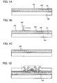
- the softened region of the glass substrate is solidified as shown in FIG 2D.
- the solidified region is indicated by reference numeral 121.
- heated regions 122 are formed on both sides of the solidified region 121.
- a temperature curve 123 of the glass substrate surface irradiated with the laser beam in FIG 2E the temperature of the glass substrate surface in the solidified region 121 and in the heated regions 122 on both sides of the solidified region 121 is higher than room temperature (RT) and lower than the softening point.
- RT room temperature
- the stress of the glass substrate surface at this time is shown by a stress curve 124 in FIG 2F.
- the repetition rate be set to be greater than or equal to 1 Hz and less than 10 MHz
- the laser energy density be set to be 0.5 J/cm 2 to 5 J/cm 2 (typically 1 J/cm 2 to 2 J/cm 2 ).
- the pulse repetition rate of the laser beam is set to be greater than or equal to 1 Hz and less than 10 MHz, the pulse interval can be longer than the crystal growing time. Further, while repeating complete melting and solidification of the amorphous semiconductor film by laser beam irradiation of the present invention, a solid-liquid interface is moved and crystallization can be performed.
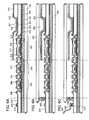
- the spot of the laser beam whose optical path is changed by the mirror 1005 is shaped in a width direction by a projection lens 1006 of which a light-condensing property (resolution) is enhanced by one or more lenses.
- the structure of the projection lens can be appropriately selected in accordance with the length in a width direction of the laser beam.
- a laser beam spot having a length in a width direction of less than or equal to 100 ⁇ m, preferably 5 ⁇ m to 50 ⁇ m can be shaped.
- the projection lens 1006 a doublet cylindrical lens can also be used as the projection lens 1006, a doublet cylindrical lens can also be used as the projection lens 1006, a doublet cylindrical lens can also be used.
- the doublet cylindrical lens means a lens including two cylindrical lenses.
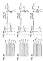
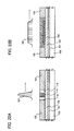
- FIG. 19A is a top view of when the amorphous semiconductor film 103 is irradiated with the laser beam 104.
- FIGS. 19B to 19F show enlarged views of a region 105a of FIG. 19A.
- the amorphous semiconductor film 103 is irradiated with a laser beam having a moving distance of the laser beams of one shot to the next shot (hereinafter, pitch 1) of, as described above, less than the crystal growth distance d, a width of less than or equal to 100 ⁇ m, preferably 5 ⁇ m to 50 ⁇ m, a steep rise in profile, and a full width at half maximum of a profile of less than or equal to 50 ⁇ m, As shown in FIG. 19F, a crystalline silicon film in which a crystal grain 163 extends in one direction, i.e., a crystalline semiconductor film in which crystals grow in a lateral direction can be formed.
- FIG. 22A shows a cross-sectional view regarding the crystal growth of the semiconductor film of the present invention and a laser beam profile.
- the cross-sectional view regarding the crystal growth of the semiconductor film is a view in a direction parallel to a scanning direction of the laser beam (shown by the arrow in the drawing).
- the amorphous semiconductor film 103 is irradiated with the laser beam 104.
- a pulsed laser beam is selected, which has a width of less than or equal to 100 ⁇ m, a ratio of width to length of 1:500 or more, and a full width at half maximum of a profile of less than or equal to 50 ⁇ m.
- a crystalline semiconductor film 105 in which crystals grow in a scanning direction of the laser beam can be formed over the insulating film 102.
- an excimer laser beam is used as the laser beam 104.
- a Ti film with a thickness of 100 nm, an A1 film with a thickness of 333 nm, and a Ti film with a thickness of 100 nm are formed in sequence by a sputtering method. Then, the films are selectively etched, using a resist mask formed by a photolithography process as a mask, to form the wirings 234 to 239 and the connection terminal 240. After that, the resist mask is removed.
- a second pixel electrode 253 is formed over a counter substrate 251, and an insulating film 254 which serves as an alignment film is formed over the second pixel electrode 253. Note that a colored film 252 may be provided between the counter substrate 251 and the second pixel electrode 253.
- a layer 318 containing a light-emitting substance is formed by an evaporation method over a part of the first electrode 316 and the organic insulating film 317.
- the layer 318 containing a light-emitting substance is formed of an organic or inorganic compound having a light-emitting property. Further, the layer 318 containing a light-emitting substance may be formed of an organic compound having a light-emitting property and an inorganic compound having a light-emitting property.
- an aromatic amine compound typified by TDATA, MTDATA, m-MTDAB, TPD, NPB, DNTPD, BBPB, TCTA, or the like is preferable as the organic compound because it easily generates holes.
- the substances mentioned here generally have a hole mobility of 10 -6 cm 2 /Vs or more.
- the aforementioned materials with an electron-transporting property may be used.
- an ultrathin film of an insulator such as the following is often used: a halide of an alkali metal, such as lithium fluoride or cesium fluoride; a halide of an alkaline-earth metal, such as calcium fluoride; or an oxide of an alkali metal, such as lithium oxide.
- an alkali metal complex such as lithium acetyl acetonate (abbr.: Li(acac)) or 8-quinolinolato-lithium (abbr.: Liq) is also effective.
- a material mixed by, for example, co-evaporating an aforementioned material with an electron-transporting property and a metal with a low work function such as Mg, Li, or Cs can also be used.
- nitride aluminum nitride, gallium nitride, indium nitride, or the like can be used, for example. Further, zinc selenide, zinc telluride, or the like can also be used. A ternary mixed crystal such as calcium gallium sulfide, strontium gallium sulfide, or barium gallium sulfide may also be used.
- the layer containing a light-emitting substance can be formed by a droplet discharging method that can selectively form the layer containing the light-emitting substance, a printing method (such as screen printing or offset printing), a coating method such as a spin coating method, a dipping method, a dispensing method, or the like.
- a printing method such as screen printing or offset printing
- a coating method such as a spin coating method, a dipping method, a dispensing method, or the like.
- the thickness of the layer is preferably in the range of 10 to 1000 nm.
- the proportion of the light-emitting material in the layer containing a light-emitting substance, which includes the light-emitting material and the binder is preferably in the range of 50 wt% to 80 wt%, inclusive.
- propylene glycolmonomethyl ether propylene glycolmonomethyl ether acetate (also called PGMEA), 3-methoxy-3-methyl-1-butanol (also called MMB), or the like can be used as the solvent.
- PGMEA propylene glycolmonomethyl ether
- MMB 3-methoxy-3-methyl-1-butanol
- an OLED 334G which emits green light is connected to a drain region of the thin film transistor 332 for driving, and an anode-side power supply line 337G is provided in a source region of the thin film transistor 332 for driving.
- the OLED 334G is provided with the cathode-side power supply line 333.
- the thin film transistor 331 for switching is connected to the gate wiring 336, and the gate electrode of the thin film transistor 332 for driving is connected to the drain region of the thin film transistor 331 for switching.
- the drain region of the thin film transistor 331 for switching is connected to the capacitor 338 which is connected to the anode-side power supply line 337G.
- Different voltages are applied to each of the pixels having different colors to one another, depending on the material of the layer containing a light-emitting substance.
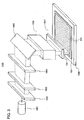
- the flexible substrate 422 is attached to a UV sheet 431 of a dicing frame 432, as shown in FIG 10C. Since the UV sheet 431 is adhesive, the flexible substrate 422 is fixed on the UV sheet 431. Subsequently, the conductive film 411 may be irradiated with a laser beam to increase adhesiveness between the conductive film 411 and the conductive film 408.
- the UV sheet 431 of the dicing frame 432 is irradiated with UV light to decrease the adhesiveness thereof.
- the UV sheet 431 is supported by an expander frame 444.
- the width of a groove 441 which is formed between the thin film integrated circuits 442a and 442b can be increased.
- a width of an expanded groove 446 is preferably decided in accordance with the size of an antenna substrate which is subsequently attached to the thin film integrated circuits 442a and 442b.
- a digital video camera shown in FIG 15B includes a display portion 9701, a display portion 9702, and the like.
- a digital video camera capable of high-definition display can be provided at a low price.
- a portable computer shown in FIG 15E includes a main body 9401, a display portion 9402, and the like.
- a portable computer capable of high-definition display can be provided at a low price.
- a pixel portion and at least one peripheral driver circuit may be formed over one glass substrate using TFTs, whereas the other peripheral driver circuits (in a plurality of driver circuits, the driver circuit which has a high operating frequency) may be formed over an IC chip.
- the IC chip may be mounted on the display panel 2701 using a COG (chip on glass) method, or the IC chip may be connected to a glass substrate by using TAB (tape automated bonding) or a printed board.
- a pixel portion may be formed over a glass substrate using TFTs and all the peripheral driver circuits may be formed over an IC chip, and then the IC chip may be mounted on a display panel using a COG (chip on glass) method or the like, as shown in FIG. 18B.
- a display panel shown in FIG. 18B includes a glass substrate 3910, a signal line driver circuit 3911, a pixel portion 3912, a scanning line driver circuit 3913, a scanning line driver circuit 3914, an FPC 3915, an IC chip 3916, an IC chip 3917, a sealing substrate 3918, and a sealant 3919.
- a semiconductor device of the present invention is compact, thin, and lightweight. With these features, the limited space within the case of the electronic device can be used efficiently. Further, cost reduction is possible, and an electronic device having a semiconductor device with high reliability can be manufactured.
Applications Claiming Priority (1)
| Application Number | Priority Date | Filing Date | Title |
|---|---|---|---|
| JP2006301810 | 2006-11-07 |
Publications (3)
| Publication Number | Publication Date |
|---|---|
| EP1921667A2 true EP1921667A2 (fr) | 2008-05-14 |
| EP1921667A3 EP1921667A3 (fr) | 2011-05-04 |
| EP1921667B1 EP1921667B1 (fr) | 2017-05-03 |
Family
ID=38912394
Family Applications (1)
| Application Number | Title | Priority Date | Filing Date |
|---|---|---|---|
| EP07021213.9A Expired - Fee Related EP1921667B1 (fr) | 2006-11-07 | 2007-10-30 | Procédé de fabrication d'un dispositif semi-conducteur |
Country Status (5)
| Country | Link |
|---|---|
| US (3) | US7811911B2 (fr) |
| EP (1) | EP1921667B1 (fr) |
| JP (1) | JP5252877B2 (fr) |
| KR (1) | KR101380136B1 (fr) |
| CN (1) | CN101179012B (fr) |
Families Citing this family (25)
| Publication number | Priority date | Publication date | Assignee | Title |
|---|---|---|---|---|
| JP5085014B2 (ja) | 2005-05-26 | 2012-11-28 | 株式会社ジャパンディスプレイイースト | 半導体装置の製造方法及び半導体装置 |
| US7615502B2 (en) * | 2005-12-16 | 2009-11-10 | Sandisk 3D Llc | Laser anneal of vertically oriented semiconductor structures while maintaining a dopant profile |
| US20090193676A1 (en) * | 2008-01-31 | 2009-08-06 | Guo Shengguang | Shoe Drying Apparatus |
| DE102008023035B4 (de) * | 2008-05-09 | 2016-01-07 | Novaled Ag | Lichtemittierendes organisches Bauelement und Verfahren zum Herstellen |
| KR20100043011A (ko) * | 2008-10-17 | 2010-04-27 | 세이코 엡슨 가부시키가이샤 | 유기 el 장치, 유기 el 장치의 제조 방법, 전자 기기 |
| CN102232239A (zh) * | 2008-11-14 | 2011-11-02 | 纽约市哥伦比亚大学理事会 | 用于薄膜结晶的系统和方法 |
| WO2010110389A1 (fr) * | 2009-03-27 | 2010-09-30 | 旭硝子株式会社 | Organopolysiloxane, composite de revêtement dur, et substrat de résine ayant une couche de revêtement dur |
| EP2239084A1 (fr) * | 2009-04-07 | 2010-10-13 | Excico France | Procédé et appareil pour l'irradiation d'une surface de matériau semi-conducteur avec de l'énergie laser |
| CN102049611B (zh) * | 2009-10-30 | 2013-11-06 | 技鼎股份有限公司 | 应用于脆性材料的镭射加工装置及镭射加工和位移补偿的方法 |
| WO2011071717A2 (fr) * | 2009-12-11 | 2011-06-16 | National Semiconductor Corporation | Compensation de contrainte sur face postérieure pour dispositifs à semi-conducteurs à base de nitrure de gallium ou d'autres nitrures |
| KR20130100996A (ko) * | 2010-08-31 | 2013-09-12 | 가부시끼가이샤 니혼 세이꼬쇼 | 레이저 어닐링 장치 및 레이저 어닐링 방법 |
| JP6140400B2 (ja) | 2011-07-08 | 2017-05-31 | エスケーハイニックス株式会社SK hynix Inc. | 半導体装置及びその製造方法 |
| JP2014006049A (ja) * | 2012-06-21 | 2014-01-16 | Sumitomo Bakelite Co Ltd | マイクロ流路チップの製造方法 |
| DE102012217633A1 (de) * | 2012-09-27 | 2014-03-27 | Osram Opto Semiconductors Gmbh | Verfahren und Vorrichtung zur Überprüfung eines optoelektronischen Bauteils auf Risse |
| US9209298B2 (en) | 2013-03-08 | 2015-12-08 | Taiwan Semiconductor Manufacturing Company, Ltd. | Metal-oxide-semiconductor field-effect transistor with extended gate dielectric layer |
| JP6727762B2 (ja) * | 2014-05-30 | 2020-07-22 | 株式会社半導体エネルギー研究所 | 発光装置及び電子機器 |
| TWI755773B (zh) | 2014-06-30 | 2022-02-21 | 日商半導體能源研究所股份有限公司 | 發光裝置,模組,及電子裝置 |
| CN106663629B (zh) * | 2014-07-21 | 2020-01-10 | 应用材料公司 | 扫描脉冲退火装置及方法 |
| CN107104138B (zh) | 2016-02-19 | 2021-04-27 | 硅显示技术有限公司 | 氧化物半导体晶体管 |
| US20190081077A1 (en) * | 2016-03-15 | 2019-03-14 | Sharp Kabushiki Kaisha | Active matrix substrate |
| KR101872421B1 (ko) * | 2016-04-12 | 2018-06-28 | 충북대학교 산학협력단 | 산화물 반도체 기반의 트랜지스터 및 그 제조 방법 |
| US10170419B2 (en) | 2016-06-22 | 2019-01-01 | International Business Machines Corporation | Biconvex low resistance metal wire |
| CN110165017B (zh) * | 2019-04-18 | 2021-08-24 | 中国科学院宁波材料技术与工程研究所 | 制备隧穿氧钝化接触结构的快速退火方法 |
| KR102170175B1 (ko) * | 2019-06-26 | 2020-10-27 | 인하공업전문대학산학협력단 | 플렉시블 디스플레이 장치 제조를 위한 가접합 캐리어 글래스-금속 호일 접합체의 제조방법 |
| US11909091B2 (en) | 2020-05-19 | 2024-02-20 | Kymeta Corporation | Expansion compensation structure for an antenna |
Citations (3)
| Publication number | Priority date | Publication date | Assignee | Title |
|---|---|---|---|---|
| US20020058366A1 (en) * | 2000-06-12 | 2002-05-16 | Seiko Epson Corporation | Thin-film semiconductor device fabrication method |
| US20040079952A1 (en) * | 1998-12-29 | 2004-04-29 | Semiconductor Energy Laboratory | Semiconductor device and method of fabricating the same |
| US20060270130A1 (en) * | 2005-05-26 | 2006-11-30 | Takeshi Sato | Semiconductor device and method for manufacturing the same |
Family Cites Families (23)
| Publication number | Priority date | Publication date | Assignee | Title |
|---|---|---|---|---|
| US5173129A (en) * | 1983-10-27 | 1992-12-22 | Kawasaki Steel Corporation | Grain-oriented silicon steel sheet having a low iron loss free from deterioration due to stress-relief annealing and a method of producing the same |
| JPS61154146A (ja) * | 1984-12-27 | 1986-07-12 | Toshiba Corp | 半導体装置の製造方法 |
| US5389450A (en) * | 1987-06-12 | 1995-02-14 | Lanxide Technology Company, Lp | Composite materials and methods for making the same |
| US5874175A (en) * | 1988-11-29 | 1999-02-23 | Li; Chou H. | Ceramic composite |
| DE69127395T2 (de) * | 1990-05-11 | 1998-01-02 | Asahi Glass Co Ltd | Verfahren zum Herstellen eines Dünnfilm-Transistors mit polykristallinem Halbleiter |
| US5578520A (en) * | 1991-05-28 | 1996-11-26 | Semiconductor Energy Laboratory Co., Ltd. | Method for annealing a semiconductor |
| JPH05182923A (ja) * | 1991-05-28 | 1993-07-23 | Semiconductor Energy Lab Co Ltd | レーザーアニール方法 |
| US5411563A (en) * | 1993-06-25 | 1995-05-02 | Industrial Technology Research Institute | Strengthening of multilayer ceramic/glass articles |
| US5640045A (en) * | 1996-02-06 | 1997-06-17 | Directed Energy, Inc. | Thermal stress minimization in power semiconductor devices |
| JP3565983B2 (ja) * | 1996-04-12 | 2004-09-15 | 株式会社半導体エネルギー研究所 | 半導体装置の作製方法 |
| AUPO347196A0 (en) * | 1996-11-06 | 1996-12-05 | Pacific Solar Pty Limited | Improved method of forming polycrystalline-silicon films on glass |
| DE69819976T2 (de) * | 1997-08-05 | 2004-09-02 | Canon K.K. | Flüssigkeitsausstosskopf, Substrat und Herstelllungsverfahren |
| JP4183786B2 (ja) * | 1997-10-17 | 2008-11-19 | 株式会社半導体エネルギー研究所 | 半導体装置の作製方法 |
| JP3978145B2 (ja) | 1998-12-29 | 2007-09-19 | 株式会社半導体エネルギー研究所 | 半導体装置の作製方法 |
| JP4653374B2 (ja) * | 2001-08-23 | 2011-03-16 | セイコーエプソン株式会社 | 電気光学装置の製造方法 |
| US6617690B1 (en) * | 2002-08-14 | 2003-09-09 | Ibm Corporation | Interconnect structures containing stress adjustment cap layer |
| JP3961398B2 (ja) * | 2002-10-30 | 2007-08-22 | 富士通株式会社 | 半導体装置 |
| JP2005012003A (ja) * | 2003-06-19 | 2005-01-13 | Sharp Corp | 結晶質半導体膜およびその製造方法 |
| JP4831961B2 (ja) * | 2003-12-26 | 2011-12-07 | 株式会社半導体エネルギー研究所 | 半導体装置の作製方法、選択方法 |
| US7282380B2 (en) * | 2004-03-25 | 2007-10-16 | Semiconductor Energy Laboratory Co., Ltd. | Method for manufacturing semiconductor device |
| JP2006100698A (ja) * | 2004-09-30 | 2006-04-13 | Toshiba Corp | 半導体装置の製造方法 |
| JP5201790B2 (ja) * | 2004-11-26 | 2013-06-05 | 株式会社半導体エネルギー研究所 | 半導体装置の作製方法 |
| US20070096107A1 (en) * | 2005-11-03 | 2007-05-03 | Brown Dale M | Semiconductor devices with dielectric layers and methods of fabricating same |
-
2007
- 2007-10-24 US US11/976,379 patent/US7811911B2/en not_active Expired - Fee Related
- 2007-10-24 JP JP2007276482A patent/JP5252877B2/ja not_active Expired - Fee Related
- 2007-10-30 EP EP07021213.9A patent/EP1921667B1/fr not_active Expired - Fee Related
- 2007-11-07 CN CN2007101860359A patent/CN101179012B/zh not_active Expired - Fee Related
- 2007-11-07 KR KR1020070113272A patent/KR101380136B1/ko active IP Right Grant
-
2010
- 2010-09-22 US US12/887,597 patent/US8017508B2/en not_active Expired - Fee Related
-
2011
- 2011-08-31 US US13/222,076 patent/US8242002B2/en active Active
Patent Citations (3)
| Publication number | Priority date | Publication date | Assignee | Title |
|---|---|---|---|---|
| US20040079952A1 (en) * | 1998-12-29 | 2004-04-29 | Semiconductor Energy Laboratory | Semiconductor device and method of fabricating the same |
| US20020058366A1 (en) * | 2000-06-12 | 2002-05-16 | Seiko Epson Corporation | Thin-film semiconductor device fabrication method |
| US20060270130A1 (en) * | 2005-05-26 | 2006-11-30 | Takeshi Sato | Semiconductor device and method for manufacturing the same |
Non-Patent Citations (3)
| Title |
|---|
| "Chap. 4 - Basics of Thin Films" In: Wolf, Tauber: "SILICON PROCESSING FOR THE VLSI ERA", 1 January 2000 (2000-01-01), Lattice Press, XP009146320, vol. 4, pages 109-123, * pages 114-117, chapter 'Stress in Thin Films' * * |
| CHANG WOO LEE ET AL: "COMPARISON OF THE STRESS BETWEEN RAPID THERMAL ANNEALED AND EXCIMER LASER ANNEALED POLYCRYSTALLINE SILICON THIN FILMS", SOLID STATE COMMUNICATIONS, PERGAMON, GB, vol. 105, no. 12, 1 March 1998 (1998-03-01), pages 777-781, XP009079684, ISSN: 0038-1098, DOI: DOI:10.1016/S0038-1098(97)10235-6 * |
| LENGSFELD P ET AL: "Stress in undoped and doped laser crystallized poly-Si", JOURNAL OF APPLIED PHYSICS, AMERICAN INSTITUTE OF PHYSICS. NEW YORK, US, vol. 91, no. 11, 1 June 2002 (2002-06-01), pages 9128-9135, XP012055357, ISSN: 0021-8979, DOI: DOI:10.1063/1.1476083 * |
Also Published As
| Publication number | Publication date |
|---|---|
| US20110312165A1 (en) | 2011-12-22 |
| JP2008141179A (ja) | 2008-06-19 |
| CN101179012B (zh) | 2011-10-05 |
| CN101179012A (zh) | 2008-05-14 |
| JP5252877B2 (ja) | 2013-07-31 |
| EP1921667B1 (fr) | 2017-05-03 |
| US7811911B2 (en) | 2010-10-12 |
| KR101380136B1 (ko) | 2014-04-01 |
| US20110014780A1 (en) | 2011-01-20 |
| US20080108206A1 (en) | 2008-05-08 |
| KR20080041596A (ko) | 2008-05-13 |
| EP1921667A3 (fr) | 2011-05-04 |
| US8017508B2 (en) | 2011-09-13 |
| US8242002B2 (en) | 2012-08-14 |
Similar Documents
| Publication | Publication Date | Title |
|---|---|---|
| EP1921667B1 (fr) | Procédé de fabrication d'un dispositif semi-conducteur | |
| US9257562B2 (en) | Semiconductor device | |
| US7935584B2 (en) | Method for manufacturing crystalline semiconductor device | |
| US7662703B2 (en) | Method for manufacturing crystalline semiconductor film and semiconductor device | |
| KR101424788B1 (ko) | 결정성 반도체막, 반도체장치 및 그들의 제조방법 | |
| US20080214021A1 (en) | Method of crystallizing semiconductor film and method of manufacturing semiconductor device | |
| JP5448315B2 (ja) | 結晶性半導体膜の作製方法 | |
| JP2008085317A (ja) | 結晶性半導体膜、及び半導体装置の作製方法 | |
| JP5311754B2 (ja) | 結晶性半導体膜、半導体装置及びそれらの作製方法 | |
| JP5255793B2 (ja) | 半導体装置の作製方法 |
Legal Events
| Date | Code | Title | Description |
|---|---|---|---|
| PUAI | Public reference made under article 153(3) epc to a published international application that has entered the european phase |
Free format text: ORIGINAL CODE: 0009012 |
|
| AK | Designated contracting states |
Kind code of ref document: A2 Designated state(s): AT BE BG CH CY CZ DE DK EE ES FI FR GB GR HU IE IS IT LI LT LU LV MC MT NL PL PT RO SE SI SK TR |
|
| AX | Request for extension of the european patent |
Extension state: AL BA HR MK RS |
|
| PUAL | Search report despatched |
Free format text: ORIGINAL CODE: 0009013 |
|
| AK | Designated contracting states |
Kind code of ref document: A3 Designated state(s): AT BE BG CH CY CZ DE DK EE ES FI FR GB GR HU IE IS IT LI LT LU LV MC MT NL PL PT RO SE SI SK TR |
|
| AX | Request for extension of the european patent |
Extension state: AL BA HR MK RS |
|
| RIC1 | Information provided on ipc code assigned before grant |
Ipc: H01L 21/02 20060101ALI20110330BHEP Ipc: H01L 21/20 20060101AFI20080121BHEP |
|
| 17P | Request for examination filed |
Effective date: 20111027 |
|
| AKX | Designation fees paid |
Designated state(s): DE FI FR GB NL |
|
| 17Q | First examination report despatched |
Effective date: 20120209 |
|
| RIC1 | Information provided on ipc code assigned before grant |
Ipc: H01L 21/02 20060101ALI20160919BHEP Ipc: H01L 21/20 20060101AFI20160919BHEP Ipc: H01L 21/268 20060101ALI20160919BHEP Ipc: H01L 27/12 20060101ALI20160919BHEP Ipc: B23K 26/073 20060101ALI20160919BHEP |
|
| RAP1 | Party data changed (applicant data changed or rights of an application transferred) |
Owner name: SEMICONDUCTOR ENERGY LABORATORY CO., LTD. |
|
| RIN1 | Information on inventor provided before grant (corrected) |
Inventor name: SHIMOMURA, AKIHISA Inventor name: MIYAIRI, HIDEKAZU Inventor name: JINBO, YASUHIRO |
|
| RAP1 | Party data changed (applicant data changed or rights of an application transferred) |
Owner name: SEMICONDUCTOR ENERGY LABORATORY CO., LTD. |
|
| GRAP | Despatch of communication of intention to grant a patent |
Free format text: ORIGINAL CODE: EPIDOSNIGR1 |
|
| INTG | Intention to grant announced |
Effective date: 20161219 |
|
| GRAS | Grant fee paid |
Free format text: ORIGINAL CODE: EPIDOSNIGR3 |
|
| GRAA | (expected) grant |
Free format text: ORIGINAL CODE: 0009210 |
|
| AK | Designated contracting states |
Kind code of ref document: B1 Designated state(s): DE FI FR GB NL |
|
| REG | Reference to a national code |
Ref country code: GB Ref legal event code: FG4D |
|
| REG | Reference to a national code |
Ref country code: DE Ref legal event code: R096 Ref document number: 602007050812 Country of ref document: DE |
|
| REG | Reference to a national code |
Ref country code: NL Ref legal event code: MP Effective date: 20170503 |
|
| PG25 | Lapsed in a contracting state [announced via postgrant information from national office to epo] |
Ref country code: FI Free format text: LAPSE BECAUSE OF FAILURE TO SUBMIT A TRANSLATION OF THE DESCRIPTION OR TO PAY THE FEE WITHIN THE PRESCRIBED TIME-LIMIT Effective date: 20170503 |
|
| PG25 | Lapsed in a contracting state [announced via postgrant information from national office to epo] |
Ref country code: NL Free format text: LAPSE BECAUSE OF FAILURE TO SUBMIT A TRANSLATION OF THE DESCRIPTION OR TO PAY THE FEE WITHIN THE PRESCRIBED TIME-LIMIT Effective date: 20170503 |
|
| REG | Reference to a national code |
Ref country code: DE Ref legal event code: R097 Ref document number: 602007050812 Country of ref document: DE |
|
| PLBE | No opposition filed within time limit |
Free format text: ORIGINAL CODE: 0009261 |
|
| STAA | Information on the status of an ep patent application or granted ep patent |
Free format text: STATUS: NO OPPOSITION FILED WITHIN TIME LIMIT |
|
| 26N | No opposition filed |
Effective date: 20180206 |
|
| GBPC | Gb: european patent ceased through non-payment of renewal fee |
Effective date: 20171030 |
|
| REG | Reference to a national code |
Ref country code: FR Ref legal event code: ST Effective date: 20180629 |
|
| PG25 | Lapsed in a contracting state [announced via postgrant information from national office to epo] |
Ref country code: GB Free format text: LAPSE BECAUSE OF NON-PAYMENT OF DUE FEES Effective date: 20171030 |
|
| PG25 | Lapsed in a contracting state [announced via postgrant information from national office to epo] |
Ref country code: FR Free format text: LAPSE BECAUSE OF NON-PAYMENT OF DUE FEES Effective date: 20171031 |
|
| PGFP | Annual fee paid to national office [announced via postgrant information from national office to epo] |
Ref country code: DE Payment date: 20201020 Year of fee payment: 14 |
|
| REG | Reference to a national code |
Ref country code: DE Ref legal event code: R119 Ref document number: 602007050812 Country of ref document: DE |
|
| PG25 | Lapsed in a contracting state [announced via postgrant information from national office to epo] |
Ref country code: DE Free format text: LAPSE BECAUSE OF NON-PAYMENT OF DUE FEES Effective date: 20220503 |