EP1906485A1 - Geschichteter Filter - Google Patents
Geschichteter Filter Download PDFInfo
- Publication number
- EP1906485A1 EP1906485A1 EP07018969A EP07018969A EP1906485A1 EP 1906485 A1 EP1906485 A1 EP 1906485A1 EP 07018969 A EP07018969 A EP 07018969A EP 07018969 A EP07018969 A EP 07018969A EP 1906485 A1 EP1906485 A1 EP 1906485A1
- Authority
- EP
- European Patent Office
- Prior art keywords
- resonators
- resonator
- quarter
- stacked
- wave
- Prior art date
- Legal status (The legal status is an assumption and is not a legal conclusion. Google has not performed a legal analysis and makes no representation as to the accuracy of the status listed.)
- Withdrawn
Links
- 239000004020 conductor Substances 0.000 claims description 82
- 230000008878 coupling Effects 0.000 description 31
- 238000010168 coupling process Methods 0.000 description 31
- 238000005859 coupling reaction Methods 0.000 description 31
- 230000004048 modification Effects 0.000 description 18
- 238000012986 modification Methods 0.000 description 18
- 230000005540 biological transmission Effects 0.000 description 17
- 238000009826 distribution Methods 0.000 description 13
- 230000005684 electric field Effects 0.000 description 10
- 230000001965 increasing effect Effects 0.000 description 9
- 230000000052 comparative effect Effects 0.000 description 8
- 238000010586 diagram Methods 0.000 description 5
- 230000008901 benefit Effects 0.000 description 4
- 230000002146 bilateral effect Effects 0.000 description 4
- 239000000758 substrate Substances 0.000 description 4
- 230000007423 decrease Effects 0.000 description 3
- 230000003247 decreasing effect Effects 0.000 description 3
- 230000001413 cellular effect Effects 0.000 description 2
- 238000004891 communication Methods 0.000 description 2
- 238000000034 method Methods 0.000 description 2
- 230000009467 reduction Effects 0.000 description 2
- 230000004075 alteration Effects 0.000 description 1
- 230000000694 effects Effects 0.000 description 1
- 230000002708 enhancing effect Effects 0.000 description 1
- 230000002093 peripheral effect Effects 0.000 description 1
- 230000001902 propagating effect Effects 0.000 description 1
- 238000000926 separation method Methods 0.000 description 1
- 230000008054 signal transmission Effects 0.000 description 1
Images


Classifications
-
- H—ELECTRICITY
- H01—ELECTRIC ELEMENTS
- H01P—WAVEGUIDES; RESONATORS, LINES, OR OTHER DEVICES OF THE WAVEGUIDE TYPE
- H01P1/00—Auxiliary devices
- H01P1/20—Frequency-selective devices, e.g. filters
- H01P1/201—Filters for transverse electromagnetic waves
- H01P1/203—Strip line filters
- H01P1/20327—Electromagnetic interstage coupling
- H01P1/20336—Comb or interdigital filters
- H01P1/20345—Multilayer filters
Definitions
- the present invention relates to a small stacked filter usable in radio communication equipments such as cellular (portable) phones.
- resonators are formed by using strip conductors, and a plurality of these resonators are coupled to each other to configure a filter.
- Japanese Unexamined Patent Application Publication No. 6-216605 discloses a strip line filter where resonators constructed of strip conductors are arranged in a plane direction and interdigital coupled to each other.
- miniaturization and higher performance of radio communication equipments such as cellular phones are advanced in the recent years, and there is a demand for miniaturization of filters mounted thereon.
- the abovementioned strip line filter has difficulties in miniaturization because the resonators are planarly configured.
- As a filter advantageous in miniaturization there is, for example, a stacked filter where conductors for resonators are stacked in the inside of a dielectric substrate, as disclosed in Japanese Patent No. 3067612 .
- interdigital type resonators In the stacked filters, the use of interdigital type resonators is advantageous in the interests of miniaturization.
- the following technique can be considered. That is, conductors for a resonator are arranged in a stacking direction in a stacked substrate and then strongly interdigital coupled to each other in the stacking direction, thereby generating two operation modes. By operating in one mode having a lower frequency than the other, the physical length of the resonator can be reduced with respect to the operation frequency, thereby miniaturizing the filter.
- the impedance of a resonator connected becomes higher as the physical length of the resonator is larger.
- the impedance also becomes higher as the permittivity in the stacked substrate is smaller and the degree of capacitive coupling of the resonator is smaller.
- a small physical length of the resonator and a large degree of capacitive coupling of the resonator are advantageous in the interests of miniaturization of the stacked filter. Consequently, when an attempt is made to miniaturize the stacked filter, the impedance of the resonator may be lowered, and the impedance matching with the external circuit cannot be obtained in the passing band of the filter, failing to obtain sufficient filter characteristics. This is the primary problem when widening the band.
- the stacked filter of an embodiment of the invention includes: an array of more than two resonant sections arranged parallel in a stack plane direction, the resonant sections adjacent each other being electromagnetically coupled; a first resonator electromagnetically coupled to the resonant section on one end of the array of the resonant sections, and a second resonator electromagnetically coupled to the resonant section on the other side thereof.
- Each of the resonant sections has a plurality of quarter-wave resonators facing each other in a stacking direction, and the quarter-wave resonators facing each other are interdigital coupled to each other, so that a passing frequency as a filter is set to a value f 2 lower than a frequency f 0 determined by a physical length ⁇ 0 /4 in each of the quarter-wave resonator, and the first and second resonators have a physical length of ⁇ 2 /4, where ⁇ 2 is a wavelength corresponding to the passing frequency f 2 .
- a pair of interdigital coupled quarter-wave resonators means resonators electromagnetically coupled to each other by arranging so that the open end of a first quarter-wave resonator is faced to the short-circuit end of a second quarter-wave resonator, and the short-circuit end of the first quarter-wave resonator is faced to the open end of the second quarter-wave resonator.
- miniaturization can be facilitated by configuring the adjacent quarter-wave resonators as a pair of interdigital coupled quarter-wave resonators in the respective resonant sections.
- first and second resonance modes with respect to a resonance frequency f 0 determined by a physical quarter-wave length ⁇ 0 /4 (i.e. a resonance frequency in each of the quarter wave resonators when no interdigital coupling is established). That is, the first resonance mode resonates at a first resonance frequency f 1 higher than the resonance frequency f 0 .
- the second resonance mode resonates at a second resonance frequency f 2 lower than the resonance frequency f 0 .
- the resonance frequency is then divided into two.
- a passing frequency an operating frequency
- miniaturization can be facilitated than the case of setting the passing frequency to the resonance frequency f 0 .
- a current i flows in the same direction to each resonator, and the conductor thickness can be increased artificially, thereby reducing the conductor loss.
- the first and second resonators having a physical length of ⁇ 2 /4 are electromagnetically coupled to the resonant sections at the opposite ends of the array of the two or more resonant sections having the abovementioned interdigital coupling structure, respectively. Since ⁇ 2 is a wavelength corresponding to the passing frequency f 2 , the physical length ⁇ 2 /4 of the first and second resonators is longer than the physical length ⁇ 0 /4 of the pair of interdigital coupled quarter-wave resonators. Hence, the first and second resonators have higher impedance than the resonant sections having the interdigital coupling structure, and therefore it is easy to obtain impedance matching with external circuits in a broad band. This achieves miniaturization as the entire filter, and also provides excellent filter characteristics in the broad band.
- each of the first and second resonators has a plurality of line conductors arranged in the stacking direction and a connection conductor completing continuity between the plurality of line conductors.
- a whole length of the line conductors and the connection conductor may be a length of ⁇ 2 /4.
- the line conductors constituting the first and second resonators can be formed separately in the stacking direction, permitting a reduction of the length of the line conductors in the respective stack plane. This is advantageous in miniaturization.
- each of the first and second resonators has one end as an open end and the other end as a short-circuit end, the open end of the first resonator and the open end of the second resonator being oriented in reverse direction.
- the signal input to and the signal output from the first and second resonators may cause unnecessary pass at the open ends in the first and second resonators. That is, by oppositely orienting the open ends of the first and second resonators, the unnecessary pass can be suppressed to provide more excellent filter characteristics. In particular, attenuation poles can be generated beyond the passing frequency band. This is advantageous in improving attenuation characteristics.
- the miniaturization can be facilitated in the point that the respective resonant sections are constructed of the plurality of stacked interdigital coupled quarter-wave resonators.
- the first and the second resonators are arranged adjacent the resonant sections at the opposite ends, respectively, so that the physical length thereof can be longer than that of the plurality of interdigital coupled quarter-wave resonators.
- This enables the first and second resonators to have higher impedance than the resonant sections having the interdigital coupling structure, making it easy to obtain impedance matching with the external circuits in the broad band.
- Fig. 1 illustrates an example of the configuration of a stacked filter according to a preferred embodiment of the present invention.
- Fig. 2 illustrates the cross-sectional configuration of the stacked filter viewed from the X1 direction, taking along the YZ plane including the B-B line in Fig. 1.
- Fig. 3 illustrates the cross-sectional configuration of the stacked filter taken along the YX plane including the A-A line in Fig. 1.
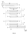
- Figs. 4A to 4F illustrate a stack plane configuration in individual layers of the stacked filter, respectively. Below the uppermost layer of Fig. 4A, the layers of Figs. 4B, 4C, 4D, 4E, and 4F as the lowermost layer, are stacked in the order named.
- the present embodiment describes an unbalanced input/unbalanced output filter having unbalanced terminals on input and output terminals thereof, respectively.
- the stacked filter includes an array of n (n is 2 or more) resonant sections 11, 12, ⁇ 1n, the adjacent ones being electromagnetically coupled to each other; a first resonator 41 electromagnetically coupled to the resonant section 11 on one end of the array of these resonant sections 11, 12, ⁇ 1n, and a second resonator 51 electromagnetically coupled to the resonant section In on the other end side thereof.
- a first external terminal electrode 1 for signals, which becomes one unbalanced terminal, is connected to the first resonator 41.
- a second external terminal electrode 2 for signals which becomes the other unbalanced terminal, is connected to the second resonator 51.
- An external circuit such as an IC (not shown) is connected to the first external terminal electrode 1 for signals or the second external terminal 2 for signals.
- This filter can serve as an unbalanced input/unbalanced output filter as a whole, by using, for example, the first external terminal electrode 1 for signals as an input terminal, and the second external terminal electrode 2 for signals as an output terminal.
- the resonant section 11 has two quarter-wave resonators 21 and 31.
- other resonators 12, ⁇ 1n have two quarter-wave resonators 22, ⁇ 2n, and 32, ⁇ 3n, respectively.
- the corresponding two quarter-wave resonators 21, 22, ⁇ 2n, and 31, 32, ⁇ 3n in the array of the resonant sections 11, 12, ⁇ 1n are interdigital coupled to each other.
- the interdigital coupling means that a pair of quarter-wave resonators 21 and 31 are electromagnetically coupled by employing one ends of these resonators 21 and 31 as open ends, and the other ends as short-circuit ends, respectively, and by arranging so that the open end of the resonator 21 is faced to the short-circuit end of the resonator 31, and the short-circuit end of the resonator 21 is faced to the open end of the resonator 31.
- the pair of quarter-wave resonators 21 and 31 are strongly interdigital coupled at the time of resonance, as will be described later. Therefore, these resonators 21 and 31 have a first resonance mode that resonates at a first resonance frequency f 1 , and a second resonance mode that resonates at a second resonance frequency f 2 lower than the first resonance frequency f 1 . More specifically, these have the first resonance frequency f 1 higher than a resonance frequency f 0 , and the second resonance frequency f 2 lower than the resonance frequency f 0 , where f 0 is a resonance frequency in each of these quarter-wave resonators 21 and 31 when no interdigital coupling is established. It is configured so that the operating frequency becomes the second resonance frequency f 2 .
- resonant sections 12, ⁇ 1n have the interdigital coupling structure.
- the stacked filter establishes electromagnetic coupling by the resonance of the adjacent resonant sections at the second resonance frequency f 2 of the lower frequency. This results in a band pass filter as a whole, using the second resonance frequency f 2 as a passing frequency. That is, the passing frequency of the filter is set to the value f 2 lower than the frequency f 0 determined by the physical length ⁇ 0 /4 of each quarter-wave resonator in each resonant section.
- the first resonator 41 has its physical length of ⁇ 2 /4, where ⁇ 2 is a wavelength corresponding to the passing frequency f 2 .
- the same is true for the second resonator 51. That is, the first and second resonators 41 and 51 are quarter-wave resonators having a length ( ⁇ 2 /4) greater than the length ( ⁇ 0 /4) of the quarter-wave resonator in the resonant sections 11, 12, ⁇ 1n.
- FIG. 1 shows a stacked filter provided with four resonant sections 11, 12, 13 and 14 (when n is 4).
- the stacked filter has a dielectric block 10 shaped like substantially a rectangular parallelepiped as a whole, as shown in Fig. 1.
- External terminal electrodes 1 and 2 for signals are formed on first opposite side surfaces of the dielectric block 10. These electrodes 1 and 2 extend to the top and bottom surfaces.
- External terminal electrodes 3 and 4 for ground are formed on second opposite side surfaces of the dielectric block 10. These electrodes 3 and 4 extend to the top and bottom surfaces.
- Conductor patterns as shown in Figs. 4B to 4E are formed as internal layers in the inside of the dielectric block 10. These internal layers are stacked under the structure as shown in Figs. 2 and 3.
- this structure can be obtained by a stacked structure, namely stacking in sequence individual sheet-shaped dielectric substrates, each having a predetermined pattern on the surface thereof.
- the stacked filter has, as internal layers, shield electrode layers (Figs. 4B and 4E) provided with shield electrodes 5 and 6, respectively, and line conductor layers (Figs. 4C and 4D) provided with line conductors for constructing the resonant sections 11, 12, 13 and 14, and the first and second resonators 41 and 51, respectively.
- the shield electrodes 5 and 6 are stacked vertically with the line conductor layer in between.
- a region 5A on the top surface, corresponding to the external terminal electrodes 1 and 2 for signals is recessed (refer to Figs. 4A and 4B).
- a region 6A on the bottom surface, corresponding to the external terminal electrodes 1 and 2 for signals is recessed (refer to Figs. 4E and 4F).
- a first group of the quarter-wave resonators 21, 22, 23 and 24, and a second group of the quarter-wave resonators 31, 32, 33 and 34 are formed as line patterns (strip lines) of the conductor. These line patterns have a length of ⁇ 0 /4, as above described.
- All of the quarter-wave resonators 21, 22, 23 and 24 in the first group are formed in a stacked surface 102 (Fig. 4D). Their respective first ends become short-circuit ends as being connected to the external terminal electrode 4 for ground, and their respective second ends are open ends, as shown in Fig. 3.
- All of the quarter-wave resonators 31, 32, 33 and 34 in the second group are formed in a stacked surface 101 (Fig.
- the first resonator 41 is constructed of a line conductor 41A (Fig. 4D) formed on the stacked surface 102, a line conductor 41B (Fig. 4C) formed on the stacked surface 101, and a feed-through conductor 7 (Fig. 2) as a connection conductor completing continuity between the line conductors 41A and 41B.
- the first resonator 41 including these line conductors 41A and 41B and the feed-through conductor 7, has a length of ⁇ 2 /4, as a whole.
- the line conductor 41A is formed adjacent the quarter-wave resonator 21 constituting the resonant section 11 on the first end side in the stacked surface 102.
- the line conductor 41B is formed adjacent the quarter-wave resonator 31 on the second end side in the stacked surface 101.
- One end of the line conductor 41A is a short-circuit end as being connected to the external terminal electrode 4 for ground, and the other end is connected to the feed-through conductor 7.
- One end of the line conductor 41B is connected to the feed-through conductor 7, and the other end is the open end.
- the line conductors 41A, 41B and the feed-through conductor 7 configure, as a whole, the quarter-wave resonator having a length of ⁇ 2 /4, one end of which is the short-circuit end and the other end is the open end.
- the second resonator 51 is constructed of a line conductor 51A (Fig. 4C) formed on the stacked surface 101, a line conductor 51B (Fig. 4D) formed on the stacked surface 102, and a feed-through conductor 8 (Fig. 2) as a connection conductor completing continuity between the line conductors 51A and 51B.
- the second resonator 51 including these line conductors 51A and 51B and the feed-through conductor 8, has a length of ⁇ 2 /4, as a whole.
- the line conductor 51A is formed adjacent the quarter-wave resonator 34 constituting the resonant section 14 on the stacked surface 101.
- the line conductor 51B is formed adjacent the quarter-wave resonator 24 on the stacked surface 102.
- One end of the line conductor 51A is a short-circuit end connected to the external terminal electrode 3 for ground, and the other end is connected to the feed-through conductor 8.
- One end of the line conductor 51B is connected to the feed-through conductor 8, and the other end is the open end.
- the line conductors 51A, 51B and the feed-through conductor 8 configure, as a whole, the quarter-wave resonator having a length of ⁇ 2 /4, one end of which is the short-circuit end and the other end is the open end.
- the line conductor 41B constituting the open end of the first resonator 41 is in continuity with one end of a leading conductor 41C formed on the stacked surface 101.
- the other end of the leading conductor 41C is in continuity with the first external terminal electrode 1 in the direction of the side surface.
- the line conductor 51B constituting the open end side of the second resonator 51 is in continuity with one end of a leading conductor 51C formed on the stacked surface 102.
- the other end of the leading conductor 51C is in continuity with the second external terminal electrode 2 in the direction of the side surface.
- the second resonator 51 is brought into continuity with the second external terminal electrode 2 from the stacked surface 102, through the leading conductor 51C. Accordingly, in the stacked filter, the first and second resonators 41 and 51 are connected to the external terminal electrodes 1 and 2 from different inside layer sides, respectively.
- the stacked filter is configured so that the open end of the first resonator 41 and the open end of the second resonator 51 are oriented in the reverse direction.
- the other end of the line conductor 41B, as the open end of the first resonator 41 is oriented in the X2 direction as shown in Fig. 4C
- the other end of the line conductor 51B as the open end of the second resonator 51 is oriented in the X1 direction as the reverse of the X2 direction, as shown in Fig. 4D.
- an unbalanced signal inputted from the first external terminal electrode 1 for signals is filtered by using the second resonance frequency f 2 as a passing band, and then outputted from the second external terminal electrode 2 for signals.
- the stacked filter enables miniaturization by configuring the respective resonant sections 11, 12, 13 and 14 as a pair of interdigital coupled quarter-wave resonators, and by using, as a passing band, the second resonance frequency f 2 having a lower frequency in the pair of interdigital coupled quarter-wave resonators.
- the pair of quarter-wave resonators are of interdigital type and strongly coupled to each other as shown in Fig.10 that will be described later, there appear first and second resonance modes with respect to a resonance frequency f 0 in each of the quarter wave resonators when no interdigital coupling is established (i.e. a resonance frequency determined by the physical quarter-wave length ⁇ 0 /4).
- the first resonance mode resonates at a first resonance frequency f 1 higher than the resonance frequency f 0 .
- the second resonance mode resonates at a second resonance frequency f 2 lower than the resonance frequency f 0 .
- the resonance frequency is then divided into two. In this case, by setting, as an operating frequency as a resonator, the second resonance frequency f 2 lower than the resonance frequency f 0 corresponding to the physical length ( ⁇ 0 /4), miniaturization can be facilitated than the case of setting the operating frequency to the resonance frequency f 0 .
- the first and second resonators 41 and 51 having a physical length of ⁇ 2 /4 are electromagnetically coupled to the resonant sections 11 and 14 at the opposite ends of the array of the plurality of resonant sections 11, 12, 13 and 14 having the abovementioned interdigital coupling structure, respectively. Since ⁇ 2 is a wavelength corresponding to the passing frequency f 2 , the physical length ⁇ 2 /4 of the first and second resonators 41 and 51 is longer than the physical length ⁇ 0 /4 of the pair of interdigital coupled quarter-wave resonators in the plurality of resonant sections 11, 12, 13 and 14.
- the first and second resonators 41 and 51 have higher impedance than the resonant sections 11, 12, 13 and 14 having the interdigital coupling structure, and therefore it is easy to obtain impedance matching with the external circuits in a broad band. This enables miniaturization as the entire filter, and also provides excellent filter characteristics in the broad band.
- the line conductor constituting the first and second resonators 41 and 51 are formed separately in the stacking direction, permitting a reduction of the line conductor length in each stack plane. This is advantageous in miniaturization.
- the open end of the first resonator 41 and the open end of the second resonator 51 are formed in different layers, and oriented in reverse direction. This provides filter characteristics superior to that when these open ends are oriented in the same direction.
- the signal input to and the signal output from the first and second resonators 41 and 51 may cause unnecessary pass at the open ends in the first and second resonators 41 and 51. That is, by arranging the open ends of the first and second resonators 41 and 51 in reverse direction, the unnecessary pass can be suppressed to provide more excellent filter characteristics.
- attenuation poles can be generated beyond the passing frequency band. This is advantageous in improving attenuation characteristics.
- the attenuation characteristics and loss characteristics of the stacked filter are shown in Fig. 12, on which the abscissa represents frequency and the ordinate represents attenuation amount.
- the curve indicated by reference numeral S21 represents the passing loss characteristics of signals in the stacked filter
- the curve indicated by reference numeral S11 represents the reflection loss characteristics when viewed from the input terminal (the external terminal electrode 1 for signals). It will be noted from Fig. 12 that excellent attenuation characteristics and loss characteristics are obtained in a broad band, and attenuations poles 201 and 202 are generated beyond the passing frequency band.
- FIG. 13 shows the attenuation characteristics and loss characteristics in the structure of a stacked filter as a comparative example of the present embodiment.
- the internal structure of the stacked filter of the comparative example are illustrated in Figs. 16A to 16F, in which those parts corresponding to the stacked filter of the present embodiment as illustrated in Figs. 4A to 4F are identified with the same numerals.
- the stacked filter of the comparative example has quarter-wave resonators 21, 22, 23, 24, 25 and 26, and quarter-wave resonators 31, 32, 33, 34, 35 and 36, which constitute six resonant sections 11, 12, 13, 14, 15 and 16.
- This filter is not provided with the first and second resonators 41 and 51 in the present embodiment, and leading conductors 41C and 51C are directly connected to the quarter-wave resonators 31 and 36 constituting the resonant sections 11 and 16 at the opposite ends, respectively.
- the open ends of the quarter-wave resonators 31 and 36, to which the leading conductors 41C and 51C are connected respectively, are oriented in the same direction.
- the structure of the comparative example not provided with the first and second resonators 41 and 51 is particularly inferior to the structure of the present embodiment in the reflection loss characteristics in the passing frequency band. Additionally, neither the attenuation pole 201 nor 202 as observed in the present embodiment is formed beyond the passing frequency band. That is, the comparative example is also inferior to the present embodiment in passing loss characteristics.
- Fig. 6 illustrates a first resonance mode in the pair of interdigital coupled quarter-wave resonators 21 and 31.
- Fig. 7 illustrates a second resonance mode thereof.
- the curves represented by the broken line illustrate distributions of an electric field E in the respective resonators.
- Figs. 6 and 7 also illustrate the state of resonance of the pair of quarter-wave resonators 21 and 31, in which the other end is grounded. This means a zero potential in alternating current.
- a current i flows from the open end to the short-circuit end in the pair of quarter-wave resonators 21 and 31, respectively, and the currents i passing through these resonators reverse in direction.
- an electromagnetic wave is excited in the same phase by the pair of quarter-wave resonators 21 and 31.
- the current i flows from the open end to the short-circuit end in one quarter-wave resonator 21, and the current i flows from the short-circuit end to the open end in the other the quarter-wave resonator 31, so that the currents i passing through these resonators flow in the same direction. That is, in the second resonance mode, an electromagnetic wave is excited in phase opposition by the pair of quarter-wave resonators 21 and 31, as can be seen from the distribution of the electric field E. In the second resonance mode, the phase of the electric field E is shifted 180 degrees at such positions as to be mutually rotation symmetry with respect to a physical axis of rotation symmetry, as a whole of the pair of quarter-wave resonators.
- the resonance frequency of the first resonance mode can be expressed by f 1 in the following equation (1A), and the resonance frequency of the second resonance mode can be expressed by f 2 in the following equation (1B).
- ⁇ f 1 c ⁇ ⁇ ⁇ r ⁇ l ⁇ tan -1 Z e
- Z o f 2 c ⁇ ⁇ ⁇ r ⁇ l ⁇ tan -1 Z o Z e
- c is a light velocity
- ⁇ r is an effective relative permittivity
- 1 is a resonator length
- Z e is a characteristic impedance of an even mode
- Z o is a characteristic impedance of an odd mode.
- a transmission mode for propagating to the transmission line can be decomposed into two independent modes of an even mode and an odd mode (these do not interfere with each other).
- Fig. 8A illustrates a distribution of the electric field E in the odd mode of the coupling transmission line
- Fig. 8B illustrates a distribution of the electric field E in the even mode.
- a ground layer 150 is formed at a peripheral portion
- conductor lines 151 and 152 of bilateral symmetry are formed in the inside.
- Figs. 8A and 8B illustrate electric field distributions within a cross section orthogonal to a transmission direction of the coupling transmission line, and the direction of transmission of a signal is orthogonal to the drawing surface.
- Fig. 9A illustrates a transmission line equivalent to that in Fig. 8A.
- a structure equivalent to the line composed only of the conductor line 151 can be obtained by replacing the symmetrical plane with the actual electrical wall 153E (a wall of zero potential, or a ground).
- the characteristic impedance by the line illustrated in Fig. 9A becomes a characteristic impedance Z 0 in the odd mode in the above-mentioned equations (1A) and (1B).
- Fig. 9B illustrates a transmission line equivalent to that in Fig. 8B.
- a structure equivalent to the line composed only of the conductor line 151 can be obtained by replacing the symmetrical plane with the actual magnetic wall 153H (a wall whose impedance is infinity).
- the characteristic impedance by the line illustrated in Fig. 9B becomes a characteristic impedance Z e in the even mode in the above-mentioned equations (1A) and (1B).
- the symmetrical plane becomes a ground (the electric wall 153E) from the line structure of Fig. 9A, and the capacity C with respect to the ground is increased. Hence, from the equation (2), the value of Z o is decreased.
- the symmetrical plane becomes the magnetic wall 153H from the line structure of Fig. 9B, and the capacity C is decreased. Hence, from the equation (2), the value of Z e is increased.
- Equations (1A) and (1B) are the resonance frequencies of the resonance modes of the pair of interdigital coupled quarter-wave resonators 21 and 31. Since the function of an arc tangent is a monotone increase function, the resonance frequency increases with an increase in a portion regarding tan -1 in the equations (1A) and (1B), and decreases with a decrease in the portion. That is, the value of the characteristic impedance Z o in the odd mode is decreased, and the value of the characteristic impedance Z e in the even mode is increased. As the difference therebetween increases, the resonance frequency f 1 of the first resonance mode increases from the equation (1A), and the resonance frequency f 2 of the second resonance mode decreases from the equation (1B).
- Fig. 10 illustrates a distribution state of resonance frequencies in the pair of interdigital coupled quarter-wave resonators 21 and 31.
- An intermediate resonance frequency f o of the first resonance frequency f 1 and the second resonance frequency f 2 is a frequency in the resonance at a quarter-wave determined by the physical length of a line (i.e. a resonance frequency in each of the quarter-wave resonators when no interdigital coupling is established).
- increasing the ratio of the symmetrical plane of the transmission paths corresponds to increasing the capacity C in the odd mode from the equation (2).
- Increasing the capacity C corresponds to enhancing the degree of coupling of a line. Therefore, in the pair of interdigital coupled quarter-wave resonators 21 and 31, a stronger coupling between the resonators causes further separation between the first resonance frequency f 1 and the second resonance frequency f 2 .
- the resonance frequency f 0 determined by the physical length of a quarter-wave can be divided into two. Specifically, there occur a first resonance mode that resonates at a first resonance frequency f 1 higher than the resonance frequency f 0 , and a second resonance mode that resonates at a second resonance frequency f 2 lower than the resonance frequency f 0 .
- the second resonance frequency f 2 of the low frequency as an operating frequency (a passing frequency if configured as a filter)
- an operating frequency a passing frequency if configured as a filter
- a filter is designed by setting 2.4 GHz band as a passing frequency
- FIGs. 11A and 11B illustrate schematically a distribution of a magnetic field H in the pair of interdigital coupled quarter-wave resonators 21 and 31.
- Figs. 11A and 11B illustrate magnetic field distributions within a cross section orthogonal to the direction of flow of the current i in the second resonance mode in the pair of quarter-wave resonators 21 and 31 as illustrated in Fig. 7.
- the direction of flow of the current i is a direction orthogonal to the drawing surface.
- the magnetic field H is distributed in the same direction (for example, in a counterclockwise direction) within the cross section in the pair of quarter-wave resonators 21 and 31.
- the present embodiment facilitates miniaturization by configuring the respective resonant sections 11, 12, 13 and 14 with the plurality of stacked interdigital coupled quarter-wave resonators.
- the first and the second resonators 41 and 51 are arranged so as to be electromagnetically coupled to the resonant sections 11 and 14 at the opposite ends, respectively, so that the physical length thereof is longer than that of the plurality of interdigital coupled quarter-wave resonators.
- This enables the first and second resonators 41 and 51 to have higher impedance than the resonant sections having the interdigital coupling structure, making it easy to obtain impedance matching with the external circuits in the broad band.
- Figs. 14A and 14B illustrate a first modification of the stacked filter.
- the abovementioned line conductor layers in Figs. 4C and 4D are replaced with those in Figs. 14A and 14B, respectively.
- the first and second resonators 41 and 51 are formed separately in the two stacked surfaces 101 and 102, respectively.
- the first and second resonators 41 and 51 are formed as a continuous line conductor only in the stacked surface 101. That is, the first resonator 41 is formed adjacent the quarter-wave resonator 31 constituting the resonant section 11 on a first end side in the stacked surface 101.
- the second resonator 51 is formed adjacent the quarter-wave resonator 34 constituting the resonant section 14 on a second end side in the stacked surface 101.
- Figs. 15A and 15B illustrate a second modification of the stacked filter.
- the first and second resonators 41 and 51 are formed as a continuous line conductor in the stacked surface 101.
- the first and second resonators 41 and 51 are formed as a continuous line conductor in the individual stacked surfaces 101 and 102, respectively. That is, the first resonator 41 is formed adjacent the quarter-wave resonator 31 constituting the resonant section 11 on a first end side in the stacked surface 101.
- the second resonator 51 is formed adjacent the quarter-wave resonator 24 constituting the resonant section 14 on a second end side in the stacked surface 102.
- the first resonator 41 is formed adjacent the quarter-wave resonator 31 constituting the resonant section 11 on a first end side in the stacked surface 101.
- the second resonator 51 is formed adjacent the quarter-wave resonator 24 constituting the resonant section 14 on a second end side in the
- the first and second resonators 41 and 51 in the structure of the second modification are connected to the external terminal electrodes 1 and 2 for signals from different internal layer sides, respectively. Additionally, like the structure in Figs. 4C and 4D, the open ends of the first and second resonators 41 and 51 are oriented in the reverse direction.
- the present invention is not limited to the above preferred embodiment and modifications, and other modifications are applicable.
- the foregoing description has been made of the case where the respective resonant sections 11, 12, ⁇ 1n are interdigital coupled by using the two quarter-wave resonators 2n and 3n, as a group.
- the respective resonant sections 11, 12, ⁇ 1n may have three or more quarter-wave resonators to obtain a structure having two or more groups of interdigital coupled resonators.
Landscapes
- Physics & Mathematics (AREA)
- Electromagnetism (AREA)
- Control Of Motors That Do Not Use Commutators (AREA)
Applications Claiming Priority (1)
| Application Number | Priority Date | Filing Date | Title |
|---|---|---|---|
| JP2006268439A JP4618441B2 (ja) | 2006-09-29 | 2006-09-29 | 積層型フィルタ |
Publications (1)
| Publication Number | Publication Date |
|---|---|
| EP1906485A1 true EP1906485A1 (de) | 2008-04-02 |
Family
ID=38754511
Family Applications (1)
| Application Number | Title | Priority Date | Filing Date |
|---|---|---|---|
| EP07018969A Withdrawn EP1906485A1 (de) | 2006-09-29 | 2007-09-26 | Geschichteter Filter |
Country Status (3)
| Country | Link |
|---|---|
| US (1) | US7525401B2 (de) |
| EP (1) | EP1906485A1 (de) |
| JP (1) | JP4618441B2 (de) |
Cited By (1)
| Publication number | Priority date | Publication date | Assignee | Title |
|---|---|---|---|---|
| US9178257B2 (en) | 2012-12-06 | 2015-11-03 | Anaren, Inc. | First and second microstrip networks stacked in an inverted arrangement to each other using an integrated support and shielding structure |
Families Citing this family (1)
| Publication number | Priority date | Publication date | Assignee | Title |
|---|---|---|---|---|
| JP4600456B2 (ja) * | 2007-09-28 | 2010-12-15 | Tdk株式会社 | フィルタ |
Citations (5)
| Publication number | Priority date | Publication date | Assignee | Title |
|---|---|---|---|---|
| US5066933A (en) * | 1989-08-30 | 1991-11-19 | Kyocera Corporation | Band-pass filter |
| US6470173B1 (en) * | 1998-09-30 | 2002-10-22 | Murata Manufacturing Co., Ltd. | Filter unit comprising a wideband bandpass filter and one band-elimination filter |
| EP1513217A1 (de) | 2003-09-04 | 2005-03-09 | TDK Corporation | Mehrschichtiges Bandpassfilter |
| US20060061438A1 (en) * | 2001-09-27 | 2006-03-23 | Toncich Stanley S | Electrically tunable bandpass filters |
| US20060255885A1 (en) * | 2005-04-25 | 2006-11-16 | Kyocera Corporation | Bandpass filter, high-frequency module, and wireless communications equipment |
Family Cites Families (13)
| Publication number | Priority date | Publication date | Assignee | Title |
|---|---|---|---|---|
| JPH03218102A (ja) * | 1990-01-23 | 1991-09-25 | Fujitsu General Ltd | インターデジタルフィルタ |
| JP2502824B2 (ja) * | 1991-03-13 | 1996-05-29 | 松下電器産業株式会社 | 平面型誘電体フィルタ |
| US5344695A (en) * | 1991-03-29 | 1994-09-06 | Ngk Insulators, Ltd. | Dielectric filter having coupling electrodes for connecting resonator electrodes, and method of adjusting frequency characteristic of the filter |
| US5412358A (en) * | 1992-02-28 | 1995-05-02 | Ngk Insulators, Ltd. | Layered stripline filter |
| US5374909A (en) * | 1992-02-28 | 1994-12-20 | Ngk Insulators, Ltd. | Stripline filter having internal ground electrodes |
| JPH06216605A (ja) | 1992-11-27 | 1994-08-05 | Sanyo Electric Co Ltd | ストリップラインフィルタ |
| EP0917235B1 (de) * | 1993-08-24 | 2003-01-22 | Matsushita Electric Industrial Co., Ltd. | Geschichtete dielektrische Antennenweiche |
| WO1995023438A1 (fr) * | 1994-02-18 | 1995-08-31 | Fuji Electrochemical Co., Ltd. | Resonateur et filtre dielectriques multicouches |
| JP3655742B2 (ja) * | 1997-12-22 | 2005-06-02 | 三菱電機株式会社 | 高周波帯域通過フィルタおよび分波器 |
| JP2000323901A (ja) * | 1999-05-07 | 2000-11-24 | Murata Mfg Co Ltd | 積層型lcフィルタ |
| JP2000323908A (ja) * | 1999-05-07 | 2000-11-24 | Murata Mfg Co Ltd | 積層型lcフィルタ |
| US6597259B1 (en) * | 2000-01-11 | 2003-07-22 | James Michael Peters | Selective laminated filter structures and antenna duplexer using same |
| KR100461719B1 (ko) * | 2002-04-25 | 2004-12-14 | 삼성전기주식회사 | 적층형 유전체 필터 |
-
2006
- 2006-09-29 JP JP2006268439A patent/JP4618441B2/ja active Active
-
2007
- 2007-09-24 US US11/902,615 patent/US7525401B2/en active Active
- 2007-09-26 EP EP07018969A patent/EP1906485A1/de not_active Withdrawn
Patent Citations (5)
| Publication number | Priority date | Publication date | Assignee | Title |
|---|---|---|---|---|
| US5066933A (en) * | 1989-08-30 | 1991-11-19 | Kyocera Corporation | Band-pass filter |
| US6470173B1 (en) * | 1998-09-30 | 2002-10-22 | Murata Manufacturing Co., Ltd. | Filter unit comprising a wideband bandpass filter and one band-elimination filter |
| US20060061438A1 (en) * | 2001-09-27 | 2006-03-23 | Toncich Stanley S | Electrically tunable bandpass filters |
| EP1513217A1 (de) | 2003-09-04 | 2005-03-09 | TDK Corporation | Mehrschichtiges Bandpassfilter |
| US20060255885A1 (en) * | 2005-04-25 | 2006-11-16 | Kyocera Corporation | Bandpass filter, high-frequency module, and wireless communications equipment |
Non-Patent Citations (2)
| Title |
|---|
| MU Y ET AL.: "A novel compact interdigital band-pass filter using multilayer cross-coupled folded quarter-wavelength resonators", IEEE MICROWAVE AND WIRELESS COMPONENTS LETTERS, vol. 15, no. 12, December 2005 (2005-12-01), pages 847 - 849 |
| MU Y ET AL: "A NOVEL COMPACT INTERDIGITAL BANDPASS FILTER USING MULTILAYER CROSS-COUPLED FOLDED QUARTER-WAVELENGTH RESONATORS", IEEE MICROWAVE AND WIRELESS COMPONENTS LETTERS, IEEE SERVICE CENTER, NEW YORK, NY, US, vol. 15, no. 12, December 2005 (2005-12-01), pages 847 - 849, XP001239538, ISSN: 1531-1309 * |
Cited By (1)
| Publication number | Priority date | Publication date | Assignee | Title |
|---|---|---|---|---|
| US9178257B2 (en) | 2012-12-06 | 2015-11-03 | Anaren, Inc. | First and second microstrip networks stacked in an inverted arrangement to each other using an integrated support and shielding structure |
Also Published As
| Publication number | Publication date |
|---|---|
| JP2008092113A (ja) | 2008-04-17 |
| US7525401B2 (en) | 2009-04-28 |
| JP4618441B2 (ja) | 2011-01-26 |
| US20080079517A1 (en) | 2008-04-03 |
Similar Documents
| Publication | Publication Date | Title |
|---|---|---|
| US7561012B2 (en) | Electronic device and filter | |
| US7541896B2 (en) | Stacked resonator and filter | |
| US7902944B2 (en) | Stacked resonator | |
| US9373876B2 (en) | Multiple-mode filter for radio frequency integrated circuits | |
| US7764147B2 (en) | Coplanar resonator and filter using the same | |
| US6177854B1 (en) | Dielectric resonator device | |
| JP4236667B2 (ja) | フィルタ | |
| JP4596266B2 (ja) | フィルタ | |
| US7525401B2 (en) | Stacked filter | |
| WO2020179046A1 (ja) | 共振器結合構造及び周波数フィルタ | |
| JP4600456B2 (ja) | フィルタ | |
| JP3820234B2 (ja) | 高周波モジュール | |
| JP4453690B2 (ja) | 誘電体フィルタ | |
| JP4930794B2 (ja) | フィルタ | |
| JP7231061B2 (ja) | 分布定数フィルタおよびマルチプレクサ | |
| JP5081283B2 (ja) | 信号伝送装置、フィルタ、ならびに基板間通信装置 | |
| JP4582340B2 (ja) | フィルタ | |
| JP2000068718A (ja) | マイクロストリップライン装置の結合構造、高周波フィルタ、送受共用器および通信装置 | |
| KR20030027793A (ko) | 공진기, 필터, 듀플렉서, 및 고주파 회로 장치 |
Legal Events
| Date | Code | Title | Description |
|---|---|---|---|
| PUAI | Public reference made under article 153(3) epc to a published international application that has entered the european phase |
Free format text: ORIGINAL CODE: 0009012 |
|
| AK | Designated contracting states |
Kind code of ref document: A1 Designated state(s): AT BE BG CH CY CZ DE DK EE ES FI FR GB GR HU IE IS IT LI LT LU LV MC MT NL PL PT RO SE SI SK TR |
|
| AX | Request for extension of the european patent |
Extension state: AL BA HR MK YU |
|
| 17P | Request for examination filed |
Effective date: 20080527 |
|
| 17Q | First examination report despatched |
Effective date: 20080701 |
|
| AKX | Designation fees paid |
Designated state(s): DE FI FR GB SE |
|
| STAA | Information on the status of an ep patent application or granted ep patent |
Free format text: STATUS: THE APPLICATION IS DEEMED TO BE WITHDRAWN |
|
| 18D | Application deemed to be withdrawn |
Effective date: 20091204 |