EP1903601B1 - Elektronischer Zeitschalter mit Schwebegattertransistoren und Verfahren zum Initialisieren desselben - Google Patents
Elektronischer Zeitschalter mit Schwebegattertransistoren und Verfahren zum Initialisieren desselben Download PDFInfo
- Publication number
- EP1903601B1 EP1903601B1 EP07116233A EP07116233A EP1903601B1 EP 1903601 B1 EP1903601 B1 EP 1903601B1 EP 07116233 A EP07116233 A EP 07116233A EP 07116233 A EP07116233 A EP 07116233A EP 1903601 B1 EP1903601 B1 EP 1903601B1
- Authority
- EP
- European Patent Office
- Prior art keywords
- mis type
- floating gate
- type device
- gate
- aging
- Prior art date
- Legal status (The legal status is an assumption and is not a legal conclusion. Google has not performed a legal analysis and makes no representation as to the accuracy of the status listed.)
- Expired - Fee Related
Links
- 238000000034 method Methods 0.000 title claims description 30
- 230000032683 aging Effects 0.000 claims description 199
- 239000004065 semiconductor Substances 0.000 claims description 91
- 239000000758 substrate Substances 0.000 claims description 43
- 101100186130 Arabidopsis thaliana NAC052 gene Proteins 0.000 claims description 35
- 101100529509 Arabidopsis thaliana RECQL4A gene Proteins 0.000 claims description 35
- 101000578349 Homo sapiens Nucleolar MIF4G domain-containing protein 1 Proteins 0.000 claims description 35
- 102100027969 Nucleolar MIF4G domain-containing protein 1 Human genes 0.000 claims description 35
- 101100203168 Saccharomyces cerevisiae (strain ATCC 204508 / S288c) SGS1 gene Proteins 0.000 claims description 35
- 101100301219 Arabidopsis thaliana RDR6 gene Proteins 0.000 claims description 28
- 238000002955 isolation Methods 0.000 claims description 26
- 101150056203 SGS3 gene Proteins 0.000 claims description 23
- -1 SGD2 Proteins 0.000 claims description 20
- 230000006870 function Effects 0.000 claims description 17
- 230000014759 maintenance of location Effects 0.000 claims description 6
- 238000002347 injection Methods 0.000 claims description 4
- 239000007924 injection Substances 0.000 claims description 4
- 238000009792 diffusion process Methods 0.000 description 62
- 229910021420 polycrystalline silicon Inorganic materials 0.000 description 28
- 229920005591 polysilicon Polymers 0.000 description 28
- 230000015654 memory Effects 0.000 description 14
- 230000004048 modification Effects 0.000 description 13
- 238000012986 modification Methods 0.000 description 13
- 238000004519 manufacturing process Methods 0.000 description 11
- 239000003990 capacitor Substances 0.000 description 10
- 230000008878 coupling Effects 0.000 description 10
- 238000010168 coupling process Methods 0.000 description 10
- 238000005859 coupling reaction Methods 0.000 description 10
- 238000003483 aging Methods 0.000 description 9
- 238000010586 diagram Methods 0.000 description 9
- 230000000694 effects Effects 0.000 description 6
- 239000012535 impurity Substances 0.000 description 5
- 230000005641 tunneling Effects 0.000 description 5
- 230000008859 change Effects 0.000 description 4
- 230000003247 decreasing effect Effects 0.000 description 3
- 230000008569 process Effects 0.000 description 3
- 230000005684 electric field Effects 0.000 description 2
- 230000007246 mechanism Effects 0.000 description 2
- 230000001419 dependent effect Effects 0.000 description 1
- 230000008030 elimination Effects 0.000 description 1
- 238000003379 elimination reaction Methods 0.000 description 1
- 230000006872 improvement Effects 0.000 description 1
- 230000003071 parasitic effect Effects 0.000 description 1
- 239000007787 solid Substances 0.000 description 1
Images


Classifications
-
- H—ELECTRICITY
- H10—SEMICONDUCTOR DEVICES; ELECTRIC SOLID-STATE DEVICES NOT OTHERWISE PROVIDED FOR
- H10B—ELECTRONIC MEMORY DEVICES
- H10B41/00—Electrically erasable-and-programmable ROM [EEPROM] devices comprising floating gates
- H10B41/30—Electrically erasable-and-programmable ROM [EEPROM] devices comprising floating gates characterised by the memory core region
- H10B41/35—Electrically erasable-and-programmable ROM [EEPROM] devices comprising floating gates characterised by the memory core region with a cell select transistor, e.g. NAND
-
- G—PHYSICS
- G04—HOROLOGY
- G04F—TIME-INTERVAL MEASURING
- G04F10/00—Apparatus for measuring unknown time intervals by electric means
- G04F10/10—Apparatus for measuring unknown time intervals by electric means by measuring electric or magnetic quantities changing in proportion to time
-
- G—PHYSICS
- G04—HOROLOGY
- G04F—TIME-INTERVAL MEASURING
- G04F13/00—Apparatus for measuring unknown time intervals by means not provided for in groups G04F5/00 - G04F10/00
-
- G—PHYSICS
- G11—INFORMATION STORAGE
- G11C—STATIC STORES
- G11C16/00—Erasable programmable read-only memories
- G11C16/02—Erasable programmable read-only memories electrically programmable
- G11C16/04—Erasable programmable read-only memories electrically programmable using variable threshold transistors, e.g. FAMOS
- G11C16/0408—Erasable programmable read-only memories electrically programmable using variable threshold transistors, e.g. FAMOS comprising cells containing floating gate transistors
- G11C16/0433—Erasable programmable read-only memories electrically programmable using variable threshold transistors, e.g. FAMOS comprising cells containing floating gate transistors comprising cells containing a single floating gate transistor and one or more separate select transistors
-
- H—ELECTRICITY
- H01—ELECTRIC ELEMENTS
- H01L—SEMICONDUCTOR DEVICES NOT COVERED BY CLASS H10
- H01L29/00—Semiconductor devices adapted for rectifying, amplifying, oscillating or switching, or capacitors or resistors with at least one potential-jump barrier or surface barrier, e.g. PN junction depletion layer or carrier concentration layer; Details of semiconductor bodies or of electrodes thereof ; Multistep manufacturing processes therefor
- H01L29/40—Electrodes ; Multistep manufacturing processes therefor
- H01L29/401—Multistep manufacturing processes
- H01L29/4011—Multistep manufacturing processes for data storage electrodes
- H01L29/40114—Multistep manufacturing processes for data storage electrodes the electrodes comprising a conductor-insulator-conductor-insulator-semiconductor structure
-
- H—ELECTRICITY
- H10—SEMICONDUCTOR DEVICES; ELECTRIC SOLID-STATE DEVICES NOT OTHERWISE PROVIDED FOR
- H10B—ELECTRONIC MEMORY DEVICES
- H10B41/00—Electrically erasable-and-programmable ROM [EEPROM] devices comprising floating gates
- H10B41/30—Electrically erasable-and-programmable ROM [EEPROM] devices comprising floating gates characterised by the memory core region
-
- H—ELECTRICITY
- H10—SEMICONDUCTOR DEVICES; ELECTRIC SOLID-STATE DEVICES NOT OTHERWISE PROVIDED FOR
- H10B—ELECTRONIC MEMORY DEVICES
- H10B69/00—Erasable-and-programmable ROM [EPROM] devices not provided for in groups H10B41/00 - H10B63/00, e.g. ultraviolet erasable-and-programmable ROM [UVEPROM] devices
Definitions
- the present invention relates to a semiconductor integrated circuit having an electronic timer being free from a battery.
- an electronic timer being free from a battery, i.e., an aging device the output of which changes with elapsed time begins to be considered to be used in fields of contents distribution, credit cards, rental digital products, rental digital software, and the like.
- the aging device has a stack gate structure constituted by a floating gate and a control gate electrode and functions as an electronic timer which measures a predetermined period by a retention (aging) of electric charges in the floating gate (for example, see JP-A 2004-172404 (KOKAI) and JP-A 2005-310824 (KOKAI)).
- a tunnel insulating film is changed in thickness to make it possible to change the aging.
- the agings of the aging devices must be set to cope with business models, respectively. Since this means that a plurality of production lines of aging devices must be installed in correspondence with the agings, the production cost increases.
- a semiconductor integrated circuit comprises a semiconductor substrate, an element isolation insulating layer formed in a surface region of the semiconductor substrate, and first and second MIS type devices isolated from each other by the element isolation insulating layer and formed in adjacent first and second element regions in a second direction orthogonal to a first direction, wherein each of the first and second MIS type devices has a stack gate structure having a floating gate and a control gate electrode, the first MIS type device functions as an aging device, and the second MIS type device functions as a control device which controls an electric charge retention characteristic of the aging device.
- a semiconductor integrated circuit comprises a semiconductor substrate, an element isolation insulating layer formed in a surface region of the semiconductor substrate, a diffusion layer of a first conductivity type formed in an element region surrounded by the element isolation insulating layer, first and second MIS type devices aligned in a first direction on the diffusion layer, and two select gate transistors arranged at two end portions of the diffusion layer in the first direction, respectively, wherein each of the first and second MIS type devices has a stack gate structure having a floating gate and a control gate electrode, the first MIS type device functions as an aging device, and the second MIS type device functions as a control device which controls an electric charge retention characteristic of the aging device.
- the aging of an aging device is controlled by two control devices which sandwich the aging device, not by the thickness of a tunnel insulating film.
- the aging device and the control device are constituted by MIS devices, respectively.
- Each of the aging device and the control device has a stack gate structure having a floating gate and a control gate electrode.
- the aging of the aging device can be controlled depending on the number of electric charges injected into the floating gate of the control device.
- the aging of the aging device can be easily changed by a simple circuit without depending on the thickness of a tunnel insulating film.
- the control device has a structure in which electric charges in the floating gate do not easily leak.
- a channel of the aging device and a diffusion layer of the control device are formed from an impurity of the same conductivity type (n/p).
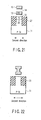
- FIG. 1 shows an example of a base unit of the aging device.
- the base unit of the aging device is constituted by a MIS device having a stack gate structure. More specifically, on a semiconductor substrate 11, a floating gate 13 is formed through a tunnel insulating film 12. On the floating gate 13, a control gate electrode 15 is formed above an inter-electrode insulating layer 14.
- the base unit of the aging device constitutes a MISFET. More specifically, in the semiconductor substrate 11, a drain diffusion layer 16 and a source diffusion layer 17 are formed, and the floating gate 13 is formed on a channel region 18 between the drain diffusion layer 16 and the source diffusion layer 17.
- the base unit is not necessarily a MISFET.
- a technique of a flash memory is used in writing (initial setting) to the base unit of the aging device.
- a potential of the control gate electrode 15 is set to be a value sufficiently higher than a potential of the channel region 18, so that electrons are injected from the channel region 18 into the control gate electrode 15 by using FN (Fowler-Nordheim) tunneling.
- the aging device measures a predetermined period of time by using aging of the number of electric charges stored in the floating gate 13, i.e., a phenomenon in which the potential of the channel region 18 changes due to leakage of electric charges. More specifically, the aging causes aging of a current (drain current Id) flowing between a drain electrode 19 and a source electrode 20.
- FIG. 2 shows four basic functions of the aging device.
- the aging of the aging device is a period of time from writing (initial setting) to a change of an output signal by electric charge leakage, and depends on an electric charge retention property.
- a point of time at which an output signal changes due to electric charge leakage is not limited to one specific point. More specifically, for example, when an aging device is structured by combining a plurality of base units, a plurality of agings can be given to the aging device.
- Table 1 Expression of forgetting Expression of remembering pMOSFET nMOSFET pMOSFET nMOSFET Type Normally-off Normally-on Operation On ⁇ off Off ⁇ on Charge Electron Hole Hole Electron
- a normally-on type realizes a function called "remembering”, while a normally-off type realizes "forgetting".
- the output signal is as shown in FIG. 2(a) .
- the output signal is as shown in FIG. 2(b) .
- the function shown in FIG. 2(c) can be realized by connecting a normally-on type base unit having a short aging and a normally-off type base unit having a long aging in series with each other.
- the function in FIG. 2(d) can be realized by connecting a normally-off type base unit having a short aging and a normally-on type base unit having a long aging in parallel to each other.
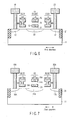
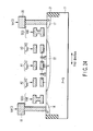
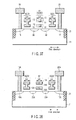
- FIG. 3 shows a plan view of a semiconductor integrated circuit according to a first embodiment.
- FIG. 4 is a sectional view along the IV - IV line in FIG. 3
- FIG. 5 is a sectional view along the V - V line in FIG. 3
- FIG. 6 is a sectional view along the VI - VI line in FIG. 3
- FIG. 7 is a sectional view along the VII VII line in FIG. 3 .
- an element isolation insulating layer 21 having an STI (shallow trench isolation) structure is formed in a semiconductor substrate 11.
- First, second, and third element regions (active areas) AA1, AA2, and AA3 are isolated from each other by the element isolation insulating layer 21 and adjacently arranged in a second direction orthogonal to a first direction.
- a width W1 in the second direction of the first element region AA1 is laid out to be smaller than widths W2 and W3 in the second direction of the second and third element regions AA2 and AA3.
- a first MIS type device A1 (SSAD: solid state aging device) functioning as an aging device and two select gate transistors SGD1 and SGS1 sandwiching the first MIS type device A1 are arranged.
- the first MIS type device A1 and the two select gate transistors SGD1 and SGS1 are connected in series with each other.
- the first MIS type device A1 has a stack gate structure. More specifically, a floating gate (FG) 13 is formed on the semiconductor substrate 11 through a tunnel insulating film 12, and a control gate electrode (CG) 15 is formed on the floating gate 13 through an inter-electrode insulating layer 14.
- FG floating gate
- CG control gate electrode
- the width W1 of the floating gate 13 in the second direction is laid out to be shorter than a length LA of the floating gate 13 in the first direction.
- a diffusion layer 22 is formed in the semiconductor substrate 11 immediately below the first MIS type device A1.
- a drain diffusion layer 16 of the select gate transistor SGD1 is connected to a drain electrode 19 through a contact plug.
- a source diffusion layer 17 of the select gate transistor SGS1 is connected to a source electrode 20 through a contact plug.
- the widths W1 of the gate electrodes of the select gate transistors SGD1 and SGS1 in the second direction are laid out to be shorter than lengths LD and LS of the gate electrodes of the select gate transistors SGD1 and SGS1 in the first direction.
- a second MIS type device A2 functioning as a control device and two select gate transistors SGD2 and SGS2 sandwiching the second MIS type device A2 are arranged.
- the second MIS type device A2 and the two select gate transistors SGD2 and SGS2 are connected in series with each other.
- the second MIS type device A2 like the first MIS type device A1, has a stack gate structure. More specifically, on the semiconductor substrate 11, a floating gate (FG) 13A is formed through a tunnel insulating film 12A. On the floating gate 13A, a control gate electrode (CG) 15A is formed through an inter-electrode insulating layer 14A.
- FG floating gate
- CG control gate electrode
- a width W2 of the floating gate 13A in the second direction is laid out to be larger than a length LA of the floating gate 13A in the first direction.
- a diffusion layer 22A is formed in the semiconductor substrate 11 immediately below the second MIS type device A2.
- a drain diffusion layer 16A of the select gate transistor SGD2 is connected to a drain electrode 19A through a contact plug.
- a source diffusion layer 17A of the select gate transistor SGS2 is connected to a source electrode 20A through a contact plug.
- a third MIS type device A3 functioning as a control device and two select gate transistors SGD3 and SGS3 sandwiching the third MIS type device A3 are arranged.
- the third MIS type device A3 and the two select gate transistors SGD3 and SGS3 are connected in series with each other.
- the structure of the third MIS type device A3 is the same as that of the second MIS type device A2, and the structures of the two select gate transistors SGD3 and SGS3 sandwiching the third MTS type device A3 are the same as those of the two select gate transistors SGD2 and SGS2 sandwiching the second MIS type device A2, so that descriptions of the structures will be omitted.
- control gate electrodes (CG) 15 and 15A of the first, second, and third MIS type devices A1, A2, and A3 are independently controlled.
- a width WI of the element isolation insulating layer 21 between the first and second element regions AA1 and AA2 in the second direction is laid out to be smaller than widths Ws in the first direction between one gate electrode of the select gate transistors SGD1, SGS1, SGD2, and SGS2 and the floating gates (FG) 13 and 13A of the first and second MIS type devices A1 and A2.
- a width WI of the element isolation insulating layer 21 between the first and third element regions AA1 and AA3 in the second direction is laid out to be smaller than widths Ws in the first direction between one gate electrode of the select gate transistors SGD1, SGS1, SGD3, and SGS3 and the floating gates (FG) 13 and 13A of the first and third MIS type devices A1 and A3.
- Lengths LA of the floating gates (FG) 13 and 13A of the first, second, and third MIS type devices A1, A2, and A3 in the first direction are laid out to be equal to each other, and lengths LD and LS of the gate electrodes of the select gate transistors SGD1, SGS1, SGD2, SGS2, SGD3, and SGS3 are laid out to be equal to each other.
- the select gate transistors SGD1, SGS1, SGD2, SGS2, SGD3, and SGS3, like the first, second, and third MIS type devices A1, A2, and A3, have stack gate structures. However, upper gate electrodes and lower gate electrodes are connected to each other by conductive plugs 999.
- the semiconductor integrated circuit can be easily formed by using manufacturing processes for a flash memory.
- the control gate electrodes (CG) 15 and 15A of the first, second, and third MIS type devices A1, A2, and A3 must be isolated from each other, mask patterns must be different from those of flash memory.
- the MIS type devices A1, A2, and A3 do not constitute MISFETs. However, for example, as shown in FIGS. 10 and 11 , the MIS type devices A1, A2, and A3 can also constitute MISFETs.
- FIGS. 8 and 9 are obtained by removing the diffusion layers 22 and 22A from FIGS. 6 and 7 .
- predetermined functions of an aging device can be realized.
- FIGS. 10 and 11 are sectional views along the first direction corresponding to FIGS. 6 and 7 . Since sectional views along the second direction are the same as FIGS. 4 and 5 , a description thereof will be omitted.
- the MIS type devices A2 and A3 are used as control devices to control the aging of the MIS type device (aging device) A1.
- a capacitive coupling Cfg between the floating gates 13 and 13A is used.
- a leakage current from the floating gate 13 is determined by a self-potential of the floating gate 13.
- the floating gate 13A of the control devices A2 and A3 can control the self-potential of the floating gate 13 of the aging device.
- the numbers of electric charges in the floating gates 13A of the MIS type devices A2 and A3 serving as control devices are adjusted to control the self-potentials of the floating gates 13. In this manner, an amount of leakage of electric charges from the floating gate 13 of the aging device A1 can be controlled.
- the capacitive coupling Cfg In order to improve the controllability of the aging of the aging device A1 by the control devices A2 and A3, the capacitive coupling Cfg must be sufficiently large.
- Writing is performed, as in a flash memory, by injecting electric charges into the floating gates 13 and 13A of the MIS type devices A1, A2, and A3.
- Control devices A2 and A3 Writing operations in the control devices A2 and A3 will be performed as follows. For example, when electrons are to be injected, at least one of the drain-side select gate transistors SGD2 and SGD3 and the source-side select gate transistors SGS2 and SGS3 is turned on, a potential of the source or the drain is transferred to the diffusion layer 22A, and a further write potential is supplied to the control gate electrode 15A.
- the writing operations in the control devices A2 and A3 may be simultaneously performed or independently performed.
- a writing operation in the aging device A1 will be performed as follows. For example, when electrons are to be injected, at least one of the drain-side select gate transistor SGD1 and the source-side select gate transistor SGS1 is turned on, the potential of the source or the drain is transferred to the diffusion layer 22, and a further write potential is supplied to the control gate electrode 15.
- the number of electric charges injected into the floating gates 13 and 13A can be controlled by a verify technique.
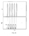
- FIG. 12 shows a technique that gradually increases a write potential Vcg to control the number of electric charges injected into the floating gates 13 and 13A.
- Rectangular pulses 1, 2, 3, 4, 5, ... the magnitudes of which gradually change are applied to the control gate electrodes 15 and 15A at predetermined intervals.
- the numbers of electric charges stored in the floating gates 13 and 13A can be investigated. For this reason, the numbers of electric charges can be accurately controlled.
- the rectangular pulses (Vcg) 1, 2, 3, 4, 5, ... to write data are supplied to the control gate electrodes 15 and 15A, or the voltage Vpass is supplied to the select gate transistors SGD1, SGS1, SGD2, SGS2, SGD3, and SGS3, until the read data reaches the expected value.
- the rectangular pulses 1, 2, 3, 4, 5, ... the ranges of which gradually change are applied to the control gate electrodes 15 and 15A at predetermined intervals.
- the rectangular pulses 1, 2, 3, 4, 5, ... in which the magnitudes and the ranges of the write potentials Vcg are constant may be applied to the control gate electrodes 15 and 15A at predetermined intervals.
- the numbers of electric charges injected into the floating gates 13 and 13A can be accurately controlled for the aging device A1 and the control devices A2 and A3.
- controllability of the control devices can be improved, and an error of the aging of the aging device can also be decreased.
- the aging of the control device In order to improve the controllability of the aging of the aging device, the aging of the control device must be longer than the aging of the aging device.
- the thickness of the tunnel insulating film of the control device may be larger than the thickness of the tunnel insulating film of the aging device.
- the thicknesses of the tunnel insulating films of the control device and the aging device are made equal to each other, and the following configuration is used as an effective means.
- the volume of the floating gate of the control device is made larger than the volume of the floating gate of the aging device.
- the conductivity type of the floating gate is made different from the conductivity type of a diffusion layer in the semiconductor substrate immediately below the floating gate in the control devices, and the conductivity type of the floating gate is made equal to the conductivity type of the diffusion layer in the semiconductor substrate immediately below the floating gate in the aging device.
- the agings of the aging device and the control device are determined by amounts of leakage of electric charges from the floating gates.
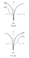
- FIGS. 15 and 16 show JV characteristics of MOS capacitors each constituted by a well region, a floating gate, and an oxide layer formed therebetween.
- the floating gate consists of an N-type polysilicon (N+poly).
- the floating gate consists of a P-type polysilicon (P+poly).
- a leakage current generated when a MOS capacitor is constituted by a pair of a P-type well region (P-Well) and an N-type polysilicon (N+poly) is smaller than a leakage current generated when the MOS capacitor is constituted by a pair of an N-type well region (N-Well) and an N-type polysilicon (N+poly).
- a leakage current generated when a MOS capacitor is constituted by a pair of an N-type well region (N-Well) and a P-type polysilicon (P+poly) is smaller than a leakage current generated when the MOS capacitor is constituted by a pair of a P-type well region (P-Well) and a P-type polysilicon (P+poly).
- FIGS. 6 and 7 will be exemplified below. That is, when the diffusion layers 22 and 22A are of N-types, the floating gate 13 of the aging device A1 is constituted by an N-type polysilicon layer, and the floating gates 13A of the control devices A2 and A3 are constituted by P-type polysilicon layers.
- the floating gate 13 of the aging device A1 is constituted by a P-type polysilicon layer
- the floating gates 13A of the control devices A2 and A3 are constituted by N-type polysilicon layers.
- the conductivity type of the floating gate 13 of the aging device A1 and the conductivity type of the floating gates 13A of the control devices A2 and A3 are different from each other.
- the conductivity types of the floating gates 13 and 13A can be made equal to each other.
- the floating gate 13 of the aging device A1 and the floating gates 13A of the control devices A2 and A3 are constituted by N-type polysilicon layers, respectively.
- the floating gate 13 of the aging device A1 and the floating gates 13A of the control devices A2 and A3 are constituted by P-type polysilicon layers, respectively.
- a negative potential can be supplied to the control gate electrodes 15 and 15A, and holes can be injected into the floating gates 13 and 13A.
- a state obtained after the hole injection is given by Vg > 0 in FIG. 16 .
- the diffusion layer 22 in FIG. 6 can also be omitted.
- the MIS type devices in FIGS. 3 to 7 are of enhancement types.
- an aging device is of a normally-on type in Table 1.
- the MIS type device In order to realize the normally-off type aging device, the MIS type device must be of a depletion type. In this case, a leakage current may be in danger of being excessively large.
- a counter doping technique can decrease an impurity concentration of the channel region.
- an impurity is doped in the channel region of the aging device A1 (SSAD) to obtain a counter doping region 23.
- N-Well N-type well region
- P-Well P-type well region
- the volumes of the floating gates 13A of the control devices A2 and A3 are made larger than the volume of the floating gate 13 of the aging device A1 as much as possible, so that a leakage current difference (difference in aging) can be sufficiently assured.
- a structure in FIG. 18 is compatible with the counter doping technique. However, in terms of improvement of controllability of aging of the aging device, the structure need not be used together with the counter doping technique.
- the structure in FIG. 18 can be easily obtained by applying a manufacturing technique for a flash memory.
- first, second, and third conductive polysilicon layers (1st Poly/2nd Poly/3rd Poly) are stacked, the first, second, and third conductive polysilicon layers may be patterned.
- the first and second conductive polysilicon layers on the first element region AA1 serve as the floating gate 13 and the control gate electrode 15, respectively.
- the first and second conductive polysilicon layers on the second and third element regions AA2 and AA3 are coupled to each other by a plug to serve as the floating gate 13A, and the third conductive polysilicon layer serves as the control gate electrode 15A.
- the normally-off type aging device can be easily realized in the structures shown in FIGS. 10 and 11 .
- FIG. 19 shows a structure of another case using the aging device A1 in FIG. 10 as a normally-off type aging device.
- the semiconductor substrate 11 is of a P-type, a well region 24 is of an N-type, and the diffusion layers 16, 17, and 22 are of P-types.
- the floating gate 13 and the control gate electrode 15 are constituted by N-type conductive polysilicon layers.
- a ground potential is applied to a channel region, and a positive write potential is applied to the control gate electrode 15. At this time, electrons are injected from the channel region into the floating gate 13 by FN tunneling.
- the channel region of the MIS type device (MISFET) A1 is inverted from an N-type to a P-type. For this reason, the MIS type device A1 is in an on state.
- the electrons in the floating gate 13 are discharged with elapse of time.
- the channel region of the MIS type device A1 returns from the P-type to the N-type, and the MIS type device A1 is turned off.
- the point of time at which the MIS type device A1 is turned off corresponds to the end of the aging.
- the normally-off type aging device can be realized by using the structure in FIG. 19 .
- the semiconductor substrate 11 is of an N-type
- the well region 24 is of a P-type
- the diffusion layers 16, 17, and 22 are of N-types
- the floating gate 13 and the control gate electrode 15 are constituted by P-type conductive polysilicon layers. Even in this case, the normally-off type aging device can be realized.
- writing is performed by applying a ground potential to the channel region, applying a negative write potential to the control gate electrode 15, and injecting holes into the floating gate 13.
- the channel region of the MIS type device (MISFET) A1 is inverted from the P-type to the N-type. For this reason, the MIS type device A1 is in an on state.
- the holes in the floating gate 13 are discharged with elapse of time. At a certain point of time, the channel region of the aging device A1 returns from the N-type to the P-type, and the aging device A1 is turned off.
- Verify reading will be described below with reference to the normally-on aging devices in FIGS. 6 and 7 .
- the semiconductor substrate 11 is of an N-type, the diffusion layers 16, 17, and 22 are of P-types, and the floating gate 13 and the control gate electrode 15 are constituted by P-type conductive polysilicon layers.
- the channel region When the write pulses are applied to the control gate electrode 15, for example, the channel region must have a ground potential. For this reason, at least one of the select gate transistors SGD1 and SGS1 is turned on, and the ground potential is transferred to the channel region.
- the verifying may be repeatedly performed to adjust the aging after writing in the control device and the verifying is completed.
- the life time of the aging device becomes short. For this reason, even though the thicknesses of the tunnel insulating films of the control device and the aging device are equal to each other, the aging (life time) of the aging device can be controlled.
- the leakage characteristics are inspected before shipping. According to the result, conditions for a method of writing (injection of electric charges) in the control device can be controlled.
- a user depending on the object, can set the aging of an aging device by using the above conditions, and an aging error generated by manufacturing fluctuation can be suppressed.
- An end user who has purchased an aging device-mounted product can use the product only during a predetermined period set by a product supplier without knowing the circumstances. More specifically, even if the end user connects the product to a network or disconnects the product from an external power supply, the user cannot use the product beyond the expiration date.
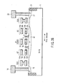
- FIG. 20 is a plan view of a semiconductor integrated circuit according to a second embodiment.
- FIG. 21 is a sectional view along the XIX - XIX line in FIG. 20
- FIG. 22 is a sectional view along the XX - XX line in FIG. 20
- FIG. 23 is a sectional view along the XXI - XXI line in FIG. 20 .
- an array of the control device, the aging device, and the control device arranged in the order named is formed through the element isolation insulating layer.
- an array of a control device, an aging device, and a control device arranged in the order named is formed in one element region.
- an element isolation insulating layer 21 having an STI structure is formed in the semiconductor substrate 11.
- An element region (active area) AA is surrounded by the element isolation insulating layer 21.
- the width of the element region (active area) AA in the second direction is set as W1.
- a first MIS type device A1 functioning as an aging device, and second and third MIS type devices A2 and A3 serving as control devices sandwiching the first MIS type device A1 are arranged.
- two select gate transistors SGD and SGS which sandwich the first, second, and third MIS type devices A1, A2, and A3 are arranged.
- the first, second, and third MIS type devices A1, A2, and A3 and the two select gate transistors SGD and SGS are connected in series with each other.
- the first MIS type device A1 has a stack gate structure. More specifically, a floating gate 13 is formed on the semiconductor substrate 11 through a tunnel insulating film 12, and a control gate electrode 15 is formed on the floating gate 13 through an inter-electrode insulating layer 14.
- the length of the floating gate 13 in the first direction is set as L1, and the width thereof in the second direction is set as W1.
- the second and third MIS type devices A2 and A3, like the first MIS type device A1, have stack gate structures. More specifically, as shown in FIG. 23 , a floating gate 13A is formed on the semiconductor substrate 11 through a tunnel insulating film 12A, and a control gate electrode 15A is formed on the floating gate 13A through an inter-electrode insulating layer 14A.
- the tunnel insulating film 12A and the inter-electrode insulating layer 14A are desirably in common with the tunnel insulating film 22 and the inter-electrode insulating layer 14.
- the length of the floating gate 23A in the first direction is set as L2 or L3, and the width thereof in the second direction is set as W1.
- a diffusion layer 22 is formed in the semiconductor substrate 11 immediately below the first, second, and third MIS type devices A1, A2, and A3.
- a drain diffusion layer 16 of the select gate transistor SGD is connected to a drain electrode 19 through a contact plug.
- a source diffusion layer 17 of the select gate transistor SGS is connected to a source electrode 20 through a contact plug.
- the select gate transistors SGD and SGS, as in the first, second, and third MIS type devices A1, A2, and A3, have stack gate structures. However, an upper gate electrode and a lower gate electrode are connected to each other by a conductive plug.
- control gate electrodes 15 and 15A of the first, second, and third MIS type devices A1, A2, and A3 are independently controlled.
- the diffusion layer 22 and the floating gate 13 are set to be of the same conductivity type, and the diffusion layer 22 and the floating gate 13A are set to be of different conductive types.
- the semiconductor substrate is of a P-type, and the diffusion layers 16, 17, and 22 are of N-types.
- the floating gate 13 is constituted by an N + -type polysilicon layer, and the floating gate 13A is constituted by a P + -type polysilicon layer.
- the aging of the aging device A1 can be controlled by using the number of electric charges injected into the control devices A2 and A3.
- the semiconductor integrated circuit as described above, as in the first embodiment, can be easily formed by using manufacturing processes for a flash memory. Since the control gate electrodes 15 and 15A of the first, second, and third MIS type devices A1, A2, and A3 must be isolated from each other, mask patterns must be different from those of flash memory.
- One of the characteristic features of the second embodiment is that the conductivity type of the floating gate of the first MIS type device A1 serving as an aging device and the conductivity types of the floating gates of the MIS type devices A2 and A3 serving as control devices are different from each other.
- a writing operation (initial setting) in the control device is performed first. Thereafter, a writing operation in the aging device is preferably performed. This order is to avoid both the writing operations from being simultaneously performed. As long as the writing operations are not simultaneously performed, the order may be reversed.
- the verify technique ( FIGS. 12 to 14 ) is employed to accurately control the aging of the aging device.
- the following phenomenon may occur. That is, while writing is performed in one of the aging device and the control device, writing is feebly performed in the other.
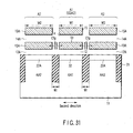
- FIG. 24 shows an example of the phenomenon.
- the example shows a manner of writing in the first MIS type device A1 serving as the aging device.
- Vd and Vs less than 0 V are applied to the drain electrode 19 and the source electrode 20, respectively.
- the select gate transistors SGD and SGS are turned on, the potentials Vd and Vs less than 0 V are transferred to the diffusion layer 22.
- a high electric field is applied to the tunnel insulating film of the first MIS type device A1, and electrons are injected from the diffusion layer 22 into the floating gate of the first MIS type device A1 by FN tunneling.
- FIG. 25 shows an example of the write-back operation.
- the magnitudes of the potentials Vprg1, Vd, and Vs are optimally set depending on the degree of write-back.
- the gate electrodes of the select gate transistors SGD and SGS are kept at the power supply voltage Vdd.
- FIG. 26 shows an example of the structures.
- a semiconductor substrate is of an N-type
- the diffusion layers 16, 17, and 22 are of P-types
- the floating gate 13 is constituted by a P + -type polysilicon layer
- the floating gate 13A is constituted by an N + -type polysilicon layer.
- the aging of the first MIS type device A1 serving as an aging device can be adjusted by the numbers of electric charges injected into the floating gates 13A of the MIS type devices A2 and A3 serving as control devices when the capacitive coupling Cfg occurring between the floating gates 13 and 13A is sufficiently large.
- the aging (life time) of the control device is sufficiently longer than the aging (life time) of the aging device, and the controllability of the aging of the aging device achieved by the control device is improved.
- FIGS. 27 and 28 show JV characteristics of MOS capacitors each constituted by a well region, a floating gate, and an oxide layer formed therebetween.
- the diffusion layer 22 is of an N-type (N-Well).
- N-Well N-type polysilicon
- the diffusion layer 22 is of a P-type (P-Well).
- a leakage current obtained when the floating gate consists of an N-type polysilicon (N+poly) is lower than that obtained when the floating gate consists of a P-type polysilicon (P+poly).
- the controllability of the aging of the aging device is improved.
- a third embodiment is a modification of the first embodiment.
- interference between the aging device and the control device is preferably increased, and interference between the aging device and the select gate transistor is preferably decreased.
- the width of the floating gate of the first MIS type device A1 serving as the aging device in a first direction is larger than the width thereof in the second direction.
- dents on both the sides of a floating gate of an aging device in a first direction are provided to increase the interference between the aging device and the control device and to decrease the interference between the aging device and the select gate transistor.
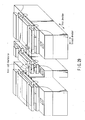
- FIG. 30 shows a plan view of a semi conductor integrated circuit according to the third embodiment.
- FIG. 31 is a sectional view along the XXXI - XXXI line in FIG. 30
- FIG. 32 is a sectional view along the XXXII - XXXII line in FIG. 30
- FIG. 33 is a sectional view along the XXXIII - XXXIII line in FIG. 30
- FIG. 34 is a sectional view along the XXXIV - XXXIV line in FIG. 30 .
- an element isolation insulating layer 21 having an STI structure is formed in a semiconductor substrate 11.
- First, second, third element regions (active areas) AA1, AA2, and AA3 are isolated from each other by the element isolation insulating layer 21 and adjacently arranged in a second direction orthogonal to a first direction.
- a width W1 of the first element region AA1 in a second direction is smaller than widths W2 and W3 of the second and third element regions AA2 and AA3 in the second direction.
- a first MIS type device (SSAD) A1 functioning as an aging device and two select gate transistors SGD1 and SGS1 sandwiching the first MIS type device A1 are arranged.
- the first MIS type device A1 and the two select gate transistors SGD1 and SGS1 are connected in series with each other.
- the first MIS type device A1 has a stack gate structure. More specifically, on the semiconductor substrate 11, a floating gate (FG) 13 is formed through a tunnel insulating film 12, and a control gate electrode (CG) 15 is formed on the floating gate 13 through an inter-electrode insulating layer 14.
- FG floating gate
- CG control gate electrode
- the width W1 of the floating gate 13 in the second direction is larger than a length LA of the floating gate 13 in the first direction.
- a width W1 of the floating gate 13 in the second direction is equal to a width of the first element region AA1. Furthermore, dents are formed on both the sides of the floating gate 13 in the first direction.
- a diffusion layer 22 is formed in the semiconductor substrate 11 immediately below the first MIS type device A1.
- a drain diffusion layer 16 of the select gate transistor SGD1 is connected to a drain electrode 19 through a contact plug.
- a source diffusion layer 17 of the select gate transistor SGS1 is connected to a source electrode 20 through a contact plug.
- the widths W1 of the gate electrodes of the select gate transistors SGD1 and SGS1 in the second direction are larger than lengths LD and LS of the gate electrodes of the select gate transistors SGD1 and SGS1 in the first direction.
- a second MIS type device A2 functioning as a control device and two select gate transistors SGD2 and SGS2 sandwiching the second MIS type device A2 are arranged.
- the second MIS type device A2 and the two select gate transistors SGD2 and SGS2 are connected in series with each other.
- the second MIS type device A2 like the first MIS type device A1, has a stack gate structure. More specifically, on the semiconductor substrate 11, a floating gate (FG) 13A is formed through a tunnel insulating film 12A. On the floating gate 13A, a control gate electrode (CG) 15A is formed through an inter-electrode insulating layer 14A.
- FG floating gate
- CG control gate electrode
- a width W2 of the floating gate 13A in the second direction is larger than a length LA of the floating gate 13A in the first direction.
- a width W2 of the floating gate 13A in the second direction is equal to the width of the second element region AA2.
- a diffusion layer 22A is formed in the semiconductor substrate 11 immediately below the second MIS type device A2.
- a drain diffusion layer 16A of the select gate transistor SGD2 is connected to a drain electrode 19A through a contact plug.
- a source diffusion layer 17A of the select gate transistor SGS2 is connected to a source electrode 20A through a contact plug.
- a third MIS type device A3 functioning as a control device and two select gate transistors SGD3 and SGS3 sandwiching the third MIS type device A3 are arranged.
- the third MIS type device A3 and the two select gate transistors SGD3 and SGS3 are connected in series with each other.
- the structure of the third MIS type device A3 is the same as that of the second MIS type device A2, and the structures of the two select gate transistors SGD3 and SGS3 sandwiching the third MIS type device A3 are the same as those of the select gate transistors SGD2 and SGS2 sandwiching the second MIS type device A2, so that descriptions of the structures will be omitted.
- control gate electrodes (CG) 15 and 15A of the first, second, and third MIS type devices A1, A2, and A3 are independently controlled.
- a width WI of the element isolation insulating layer 21 between the first and second element regions AA1 and AA2 in the second direction is smaller than widths Ws in the first direction between one gate electrode of the select gate transistors SGD1, SGS1, SGD2, and SGS2 and the floating gates (FG) 13 and 13A of the first and second MIS type devices A1 and A2.
- the width WI of the element isolation insulating layer 21 between the first and third element regions AA1 and AA3 in the second direction is smaller than the widths Ws in the first direction between one gate electrode of the select gate transistors SGD1, SGS1, SGD3, and SGS3 and the floating gates (FG) 13 and 13A of the first and third MIS type devices A1 and A3.
- Lengths LA of the floating gates (FG) 13 and 13A of the first, second, and third MIS type devices A1, A2, and A3 in the first direction are laid out to be equal to each other, and lengths LD and LS of the gate electrodes of the select gate transistors SGD1, SGS1, SGD2, SGS2, SGD3, and SGS3 in the first direction are laid out to be equal to each other.
- the select gate transistors SGD1, SGS1, SGD2, SGS2, SGD3, and SGS3, like the first, second, and third MIS type devices A1, A2, and A3, have stack gate structures. However, upper gate electrodes and lower gate electrodes are connected to each other by conductive plugs.
- the semiconductor integrated circuit as described above can be easily formed by using manufacturing processes for a flash memory. Since the control gate electrodes 15 and 15A of the first, second, and third MIS type devices A1, A2, and A3 must be isolated from each other, mask patterns must be different from those of flash memory.
- the first, second, and third MIS type devices A1, A2, and A3 do not constitute a MISFET. However, for example, as shown in FIGS. 37 and 38 , the first, second, and third MIS type devices A1, A2, and A3 may constitute a MISFET.
- FIGS. 35 and 36 are obtained by removing the diffusion layers 22 and 22A from FIGS. 37 and 38 . Even in the configurations, predetermined functions of an aging device can be realized.
- FIGS. 37 and 38 are sectional views in the first direction corresponding to FIGS. 33 and 34 . Since the sectional views in the second direction are the same as FIGS. 31 and 32 , respectively, a description thereof will be omitted.
- an aging of the first MIS type device (aging device) A1 is controlled by using the MIS type devices A2 and A3 serving as control devices.
- the capacitive coupling Cfg between the floating gates 13 and 13A is used.
- an aging (life time) of a control device In order to improve controllability of an aging (life time) of an aging device, an aging (life time) of a control device must be longer than the aging of the aging device.
- the third embodiment when the shape of the floating gate of the first MIS type transistor serving as an aging device is devised, even if the width of the floating gate of the first MIS type transistor in the first direction is not made larger than the width in the second direction unlike in the first embodiment, the same effect as that in the first embodiment can be obtained.
- a fourth embodiment is a modification of the third embodiment.
- the fourth embodiment is different from the third embodiment in widths of first element regions.
- FIG. 39 is a plan view of a semiconductor integrated circuit according to the fourth embodiment.
- FIG. 40 is a sectional view along the XL - XL line in FIG. 39
- FIG. 41 is a sectional view along the XLI - XLI line in FIG. 39 .
- FIG. 33 A sectional view along the XXXIII - XXXIII line in FIG. 39 is as shown in FIG. 33 , and a sectional view along the XXXIV - XXXIV line in FIG. 39 is as shown in FIG. 34 .
- an element isolation insulating layer 21 having an STI structure is formed in a semiconductor substrate 11.
- First, second, and third element regions (active areas) AA1, AA2, and AA3 are isolated from each other by the element isolation insulating layer 21, and adjacently arranged in a second direction orthogonal to a first direction.
- a width W1 in a second direction is smaller than widths M2 and M3 of the second and third element regions AAG and AA3 in the second direction.
- a first MIS type device (SSAD) A1 functioning as an aging device and two select gate transistors SGD1 and SGS1 sandwiching the first MIS type device A1 are arranged.
- the first MIS type device A1 and the two select gate transistors SGD1 and SGS1 are connected in series with each other.
- the first MIS type device A1 has a stack gate structure. More specifically, on the semiconductor substrate 11, a floating gate (FG) 13 is formed through a tunnel insulating film 12, and a control gate electrode (CG) 15 is formed on the floating gate 13 through an inter-electrode insulating layer 14.
- FG floating gate
- CG control gate electrode
- the width W1 of the floating gate 13 in the second direction is larger than a width of the first element region AA1. Furthermore, dents are formed on both the sides of the floating gate 13 in the first direction.
- a diffusion layer 22 is formed in the semiconductor substrate 11 immediately below the first MIS type device A1.
- a drain diffusion layer 16 of the select gate transistor SGD1 is connected to a drain electrode 19 through a contact plug.
- a source diffusion layer 17 of the select gate transistor SGS1 is connected to a source electrode 20 through a contact plug.
- the widths W1 of the gate electrodes of the select gate transistors SGD1 and SGS1 in the second direction are larger than the width of the first element region AA1.
- a second MIS type device A2 functioning as a control device and two select gate transistors SGD2 and SGS2 sandwiching the second MIS type device A2 are arranged.
- the second MIS type device A2 and the two select gate transistors SGD2 and SGS2 are connected in series with each other.
- the second MIS type device A2 like the first MIS type device A1, has a stack gate structure. More specifically, on the semiconductor substrate 11, a floating gate (FG) 13A is formed through a tunnel insulating film 12A. On the floating gate 13A, a control gate electrode (CG) 15A is formed through an inter-electrode insulating layer 14A.
- FG floating gate
- CG control gate electrode
- a width W2 of the floating gate 13A in the second direction is equal to the width of the second element region AA2.
- a diffusion layer 22A is formed in the semiconductor substrate 11 immediately below the second MIS type device A2.
- a drain diffusion layer 16A of the select gate transistor SGD2 is connected to a drain electrode 19A through a contact plug.
- a source diffusion layer 17A of the select gate transistor SGS2 is connected to a source electrode 20A through a contact plug.
- a third MIS type device A3 functioning as a control device and two select gate transistors SGD3 and SGS3 sandwiching the third MIS type device A3 are arranged.
- the third MIS type device A3 and the two select gate transistors SGD3 and SGS3 are connected in series with each other.
- the structure of the third MIS type device A3 is the same as that of the second MIS type device A2, and the structures of the two select gate transistors SGD3 and SGS3 sandwiching the third MIS type device A3 are the same as those of the select gate transistors SGD2 and SGS2 sandwiching the second MIS type device A2, so that descriptions of the structures will be omitted.
- the fourth embodiment when the shape of the floating gate of the first MIS type transistor serving as an aging device is devised, even if the wldtl'1 of the floating gate of the first MIS type transistor in the first direction is not larger than the width in the second direction unlike in the first embodiment, the same effect as that in the first embodiment can be obtained.
- a fifth embodiment is a modification of the fourth embodiment.
- the fifth embodiment is different from the fourth embodiment in widths of second and third element regions.
- FIG. 42 is a plan view of a semiconductor integrated circuit according to the fifth embodiment.
- FIG. 43 is a sectional view along the XLIII - XLIII line in FIG. 42
- FIG. 44 is a sectional view along the XLIV - XLIV line in FIG. 42 .
- FIG. 33 A sectional view along the XXXIII - XXXIII line in FIG. 42 is as shown in FIG. 33 , and a sectional view along the XXXIV - XXXIV line in FIG. 42 is as shown in FIG. 34 .
- an element isolation insulating layer 21 having an STI structure is formed in a semiconductor substrate 11.
- First, second, and third element regions (active areas) AA1, AA2, and AA3 are isolated from each other by the element isolation insulating layer 21, and adjacently arranged in a second direction orthogonal to a first direction.
- a first MIS type device (SSAD) A1 functioning as an aging device and two select gate transistors SGD1 and SGS1 sandwiching the first MIS type device A1 are arranged.
- the first MIS type device A1 and the two select gate transistors SGD1 and SGS1 are connected in series with each other.
- the first MIS type device A1 has a stack gate structure. More specifically, on the semiconductor substrate 11, a floating gate (FG) 13 is formed through a tunnel insulating film 12, and a control gate electrode (CG) 15 is formed on the floating gate 13 through an inter-electrode insulating layer 14.
- FG floating gate
- CG control gate electrode
- the width W1 of the floating gate 13 in the second direction is larger than a width of the first element region AA1. Furthermore, dents are formed on both the sides of the floating gate 13 in the first direction.
- a diffusion layer 22 is formed in the semiconductor substrate 11 immediately below the first MIS type device A1.
- a drain diffusion layer 16 of the select gate transistor SGD1 is connected to a drain electrode 19 through a contact plug.
- a source diffusion layer 17 of the select gate transistor SGS1 is connected to a source electrode 20 through a contact plug.
- the widths W1 of the gate electrodes of the select gate transistors SGD1 and SGS1 in the second direction are larger than the width of the first element region AA1.
- a second MIS type device A2 functioning as a control device and two select gate transistors SGD2 and SGS2 sandwiching the second MIS type device A2 are arranged.
- the second MIS type device A2 and the select gate transistors SGD2 and SGS2 are connected in series with each other.
- the second MIS type device A2 like the first MIS type device A1 has a stack gate structure. More specifically, on the semiconductor substrate 11, a floating gate (FG) 13A is formed through a tunnel insulating film 12A. On the floating gate 13A, a control gate electrode (CG) 15A is formed through an inter-electrode insulating layer 14A.
- FG floating gate
- CG control gate electrode
- a width W2 of the floating gate 13A in the second direction is larger than the width of the second element region AA2.
- a diffusion layer 22A is formed in the semiconductor substrate 11 immediately below the second MIS type device A2.
- a drain diffusion layer 16A of the select gate transistor SGD2 is connected to a drain electrode 19A through a contact plug.
- a source diffusion layer 17A of the select gate transistor SGS2 is connected to a source electrode 20A through a contact plug.
- Widths W2 of the gate electrodes of the select gate transistors SGD2 and SGS2 in the second direction are larger than the width of the second element region AA2.
- a third MIS type device A3 functioning as a control device and two select gate transistors SGD3 and SGS3 sandwiching the third MIS type device A3 are arranged.
- the third MIS type device A3 and the two select gate transistors SGD3 and SGS3 are connected in series with each other.
- the structure of the third MIS type device A3 is the same as that of the second MIS type device A2, and the structures of the two select gate transistors SGD3 and SGS3 sandwiching the third MIS type device A3 are the same as those of the select gate transistors SGD2 and SGS2 sandwiching the second MIS type device A2, so that descriptions of the structures will be omitted.
- the fifth embodiment when the shape of the floating gate of the first MIS type transistor serving as an aging device is devised, even if the width of the floating gate of the first MIS type transistor in the first direction is not larger than the width in the second direction unlike in the first embodiment, the same effect as that in the first embodiment can be obtained.
- the essential of the present invention is that an aging of an aging device is controlled regardless of a thickness of a tunnel insulating film by using a capacitive coupling occurring between a floating gate of a control device and a floating gate of the aging device.
- control devices is not limited to two.
- only one control device may be arranged adjacent to an aging device.
- the number of control devices may be three or more.
- the shape of a floating gate of the first MIS type transistor A1 serving as an aging device may be variously changed.
- FIG. 45 shows an example of the shapes.
- An aging device can be applied to various semiconductor integrated circuits.
- the aging device is favorably mounted together with a non-volatile semiconductor memory having a memory cell having a stack gate structure.
- a period in which reading/writing of data is permitted can be controlled by the aging device.
- the present invention can also contribute to large-capacity non-volatile semiconductor memories the agings of which can be controlled.
- an aging of an aging device can be changed by a simple circuit regardless of a thickness of a tunnel insulating film.
Claims (19)
- Integrierte Halbleiterschaltung, umfassend:ein Halbleitersubstrat (11),eine elementtrennende Isolationsschicht (21), die in einem Oberflächengebiet des Halbleitersubstrats ausgebildet ist und erste und zweite Elementgebiete in einer zu einer ersten Richtung orthogonalen zweiten Richtung trennt, underste und zweite MIS-Typ-Vorrichtungen (A1, A2, A3), die jeweils in dem ersten bzw. zweiten Elementgebiet ausgebildet sind,dadurch gekennzeichnet, daßjede der ersten und zweiten MIS-Typ-Vorrichtungen (A1, A2, A3) eine Stapel-Gatter-Struktur mit einem schwebenden Gatter und einer Steuergatterelektrode besitzen, wobei die erste MIS-Typ-Vorrichtung (A1) als eine Alterungsvorrichtung wirkt und die zweite MIS-Typ-Vorrichtung (A2, A3) als eine Steuerungsvorrichtung, welche eine (A1) elektrische Ladungserhaltungscharakteristik der Alterungsvorrichtung steuert.
- Integrierte Halbleiterschaltung nach Anspruch 1, dadurch gekennzeichnet, daß Gattersteuerungselektroden der ersten und zweiten MIS-Typ-Vorrichtungen unabhängig gesteuert sind.
- Integrierte Halbleiterschaltung nach Anspruch 1, dadurch gekennzeichnet, daß ein schwebendes Gatter der ersten MIS-Typ-Vorrichtung (A1) den gleichen Leitfähigkeitstyp wie das eines Oberflächengebietes des Halbleitersubstrats, das unmittelbar unter der ersten MIS-Typ-Vorrichtung angeordnet ist, besitzt und ein schwebendes Gatter der zweiten MIS-Typ-Vorrichtung einen Leitfähigkeitstyp besitzt, der einem Leitfähigkeitstyp eines Oberflächengebiets des Halbleitersubstrats, das unmittelbar unter der zweiten MIS-Typ-Vorrichtung (A2, A3) angeordnet ist, entgegengesetzt ist.
- Integrierte Halbleiterschaltung nach Anspruch 1, dadurch gekennzeichnet, daß eine Breite des ersten Elementgebietes in der zweiten Richtung kleiner als eine Breite des zweiten Elementgebietes in der zweiten Richtung ist.
- Integrierte Halbleiterschaltung nach Anspruch 1, dadurch gekennzeichnet, daß bei der ersten MIS-Typ-Vorrichtung (A1) eine Breite des schwebenden Gatters in der zweiten Richtung kleiner ist als eine Länge des schwebenden Gatters in der ersten Richtung.
- Integrierte Halbleiterschaltung nach Anspruch 1, dadurch gekennzeichnet, daß bei der ersten MIS-Typ-Vorrichtung (A1) Vertiefungen auf beiden Seiten des schwebenden Gatters in der ersten Richtung ausgebildet sind.
- Integrierte Halbleiterschaltung nach Anspruch 1, dadurch gekennzeichnet, daß bei der zweiten MIS-Typ-Vorrichtung (A2, A3) eine Breite des schwebenden Gatters in der zweiten Richtung größer als eine Länge des schwebenden Gatters in der ersten Richtung ist.
- Integrierte Halbleiterschaltung nach Anspruch 1, dadurch gekennzeichnet, daß jede der ersten und zweiten MIS-Typ-Vorrichtungen (A1, A2, A3) zwischen zwei Auswahl-Gatter-Transistoren (SGD1, SGS1, SGD2, SGS2, SGD3, SGS3) eingeschlossen und mit den zwei Select-Gatter-Transistoren in Reihe miteinander verbunden sind.
- Integrierte Halbleiterschaltung nach Anspruch 8, dadurch gekennzeichnet, daß eine Breite der elementtrennenden Isolationsschicht (21) zwischen dem ersten und zweiten Elementgebiet in der zweiten Richtung kleiner ist als eine Breite in der ersten Richtung zwischen einer Gatterelektrode der beiden Auswahl-Gatter-Transistoren und dem schwebenden Gatter der ersten oder zweiten MIS-Typ-Vorrichtung.
- Integrierte Halbleiterschaltung nach Anspruch 8, dadurch gekennzeichnet, daß Breiten in der zweiten Richtung der Gatterelektroden der beiden Auswahl-Gatter-Transistoren (SGD1, SGS1), die die erste MIS-Typ-Vorrichtung (A1) einschließen, kleiner als eine Länge des Gatterelektroden in der ersten Richtung sind.
- Integrierte Halbleiterschaltung nach Anspruch 1, dadurch gekennzeichnet, daß Längen der schwebenden Gatter der ersten und zweiten MIS-Typ-Vorrichtungen (A1, A2, A3) in der ersten Richtung einander gleich sind.
- Integrierte Halbleiterschaltung nach Anspruch 1, dadurch gekennzeichnet, daß von den vier Auswahl-Gatter-Transistoren (SGD1, SGS1, SGD2, SGS2, SGD3, SGS3), die die ersten und zweiten MIS-Typ-Vorrichtungen (A1, A2, A3) einschließen, Längen in der ersten Richtung der Gatterelektroden der beiden Auswahl-Gatter-Transistoren, die sich durch die elementtrennende Isolationsschicht (21) gegenüber liegen, untereinander gleich sind.
- Integrierte Halbleiterschaltung nach Anspruch 1, dadurch gekennzeichnet, daß sie ferner umfaßt:ein drittes Elementgebiet, das von den ersten und zweiten Elementgebieten durch die elementtrennende Isolationsschicht (21) getrennt und angrenzend zu dem ersten Elementgebiet ausgebildet ist, undeine dritte MIS-Typ-Vorrichtung (A2, A3), die in dem dritten Elementgebiet ausgebildet ist,wobei die zweite und dritte MIS-Typ-Vorrichtung (A2, A3) die erste MIS-Typ-Vorrichtung (A1) einschließen und die dritte MIS-Typ-Vorrichtung (A2, A3) als eine Steuerungsvorrichtung wirkt, welche eine elektrische Ladungserhaltungscharasteristik der Alterungsvorrichtung steuert.
- Integrierte Halbleiterschaltung nach Anspruch 1, dadurch gekennzeichnet, daß bei der ersten MIS-Typ-Vorrichtung (A1) eine Breite des schwebenden Gatters in der zweiten Richtung breiter ist als eine Breite des ersten Elementgebietes in der zweiten Richtung.
- Integrierte Halbleiterschaltung nach Anspruch 1, dadurch gekennzeichnet, daß bei der zweiten MIS-Typ-Vorrichtung (A2, A3) eine Breite des schwebenden Gatters in der zweiten Richtung breiter ist als die Breite des zweiten Elementgebietes in der zweiten Richtung.
- Integrierte Halbleiterschaltung nach Anspruch 1, dadurch gekennzeichnet, daß eine Breite der elementtrennenden Isolationsschicht (21) in der zweiten Richtung breiter ist als eine Breite des ersten Elementgebietes in der zweiten Richtung und eine Breite des zweiten Elementgebietes in der zweiten Richtung.
- Integrierte Halbleiterschaltung nach Anspruch 1, dadurch gekennzeichnet, daß eine Breite des schwebenden Gatters der ersten MIS-Typ-Vorrichtung (A1) in der zweiten Richtung kleiner ist als eine Breite eines schwebenden Gatters der zweiten MIS-Typ-Vorrichtung (A2, A3) in der zweiten Richtung.
- Verfahren zur Initialisierung der integrierten Halbleiterschaltung nach Anspruch 13, gekennzeichnet durch:Einspeisen elektrischer Ladungen in das schwebende Gatter der zweiten oder dritten MIS-Typ-Vorrichtung (A2, A3) unddanach Einspeisen elektrischer Ladungen in das schwebende Gatter des ersten MIS-Typ-Vorrichtung (A1) zum Beenden einer anfänglichen Einstellung.
- Verfahren nach Anspruch 18, dadurch gekennzeichnet, daß Einspeisen elektrischer Ladungen in dem schwebenden Gatter der ersten, zweiten, oder dritten MIS-Typ-Vorrichtung (A1, A2, A3) durch wiederholte Anlegung des gleichen ersten rechteckigen Impulses oder eines zweiten rechteckigen Impulses, dessen Stärke und Periode sich graduell zu der Gattersteuerungselektrode ändern, durchgeführt wird, und
unverzüglich nach dem ersten oder zweiten rechteckigen Impuls angebracht worden ist, Messen, was den Zustand der ersten oder zweiten MIS-Typ-Vorrichtung kontrolliert, durchgeführt wird und das Schreiben und das Messen wiederholt werden, bis der Zustand der ersten oder zweiten MIS-Typ-Vorrichtung ein vorgegebener Zustand wird.
Applications Claiming Priority (2)
| Application Number | Priority Date | Filing Date | Title |
|---|---|---|---|
| JP2006257752 | 2006-09-22 | ||
| JP2007186344A JP2008103675A (ja) | 2006-09-22 | 2007-07-17 | 半導体集積回路 |
Publications (3)
| Publication Number | Publication Date |
|---|---|
| EP1903601A2 EP1903601A2 (de) | 2008-03-26 |
| EP1903601A3 EP1903601A3 (de) | 2008-07-16 |
| EP1903601B1 true EP1903601B1 (de) | 2009-08-19 |
Family
ID=38801271
Family Applications (1)
| Application Number | Title | Priority Date | Filing Date |
|---|---|---|---|
| EP07116233A Expired - Fee Related EP1903601B1 (de) | 2006-09-22 | 2007-09-12 | Elektronischer Zeitschalter mit Schwebegattertransistoren und Verfahren zum Initialisieren desselben |
Country Status (4)
| Country | Link |
|---|---|
| US (1) | US7884416B2 (de) |
| EP (1) | EP1903601B1 (de) |
| JP (1) | JP2008103675A (de) |
| DE (1) | DE602007002023D1 (de) |
Families Citing this family (13)
| Publication number | Priority date | Publication date | Assignee | Title |
|---|---|---|---|---|
| JP4212622B2 (ja) | 2006-11-30 | 2009-01-21 | 株式会社東芝 | 時限スイッチ付き情報担体及び半導体集積回路 |
| JP4679528B2 (ja) | 2007-01-30 | 2011-04-27 | 株式会社東芝 | リフレッシュトリガー付き半導体記憶装置 |
| US8247861B2 (en) * | 2007-07-18 | 2012-08-21 | Infineon Technologies Ag | Semiconductor device and method of making same |
| US8320191B2 (en) | 2007-08-30 | 2012-11-27 | Infineon Technologies Ag | Memory cell arrangement, method for controlling a memory cell, memory array and electronic device |
| US7782668B2 (en) * | 2007-11-01 | 2010-08-24 | Jonker Llc | Integrated circuit embedded with non-volatile one-time-programmable and multiple-time programmable memory |
| US8580622B2 (en) * | 2007-11-14 | 2013-11-12 | Invensas Corporation | Method of making integrated circuit embedded with non-volatile programmable memory having variable coupling |
| US7787295B2 (en) * | 2007-11-14 | 2010-08-31 | Jonker Llc | Integrated circuit embedded with non-volatile multiple-time programmable memory having variable coupling |
| US7876615B2 (en) | 2007-11-14 | 2011-01-25 | Jonker Llc | Method of operating integrated circuit embedded with non-volatile programmable memory having variable coupling related application data |
| JP5221172B2 (ja) * | 2008-02-29 | 2013-06-26 | 株式会社東芝 | Nand混載型半導体時限スイッチ |
| US8305805B2 (en) * | 2008-11-03 | 2012-11-06 | Invensas Corporation | Common drain non-volatile multiple-time programmable memory |
| US8203861B2 (en) | 2008-12-30 | 2012-06-19 | Invensas Corporation | Non-volatile one-time—programmable and multiple-time programmable memory configuration circuit |
| JP2013120815A (ja) * | 2011-12-07 | 2013-06-17 | Sony Corp | Esd保護回路およびこれを備えた半導体装置 |
| US8963647B2 (en) * | 2013-02-20 | 2015-02-24 | Board Of Trustees Of Michigan State University | Self-powered timer apparatus |
Family Cites Families (12)
| Publication number | Priority date | Publication date | Assignee | Title |
|---|---|---|---|---|
| US5361227A (en) * | 1991-12-19 | 1994-11-01 | Kabushiki Kaisha Toshiba | Non-volatile semiconductor memory device and memory system using the same |
| US5760644A (en) * | 1995-10-25 | 1998-06-02 | Nvx Corporation | Integrated circuit timer function using natural decay of charge stored in a dielectric |
| JP4151229B2 (ja) * | 2000-10-26 | 2008-09-17 | ソニー株式会社 | 不揮発性半導体記憶装置およびその製造方法 |
| US6856581B1 (en) * | 2000-10-31 | 2005-02-15 | International Business Machines Corporation | Batteryless, oscillatorless, binary time cell usable as an horological device with associated programming methods and devices |
| US7075284B2 (en) * | 2002-07-08 | 2006-07-11 | Kabushiki Kaisha Toshiba | Time limit function utilization |
| JP3959340B2 (ja) | 2002-11-20 | 2007-08-15 | 株式会社東芝 | 半導体集積回路 |
| JP3822170B2 (ja) * | 2003-01-31 | 2006-09-13 | 株式会社東芝 | Icカードの利用期間設定方法、icカード、および、icカードケース |
| JP2005285818A (ja) * | 2004-03-26 | 2005-10-13 | Toshiba Corp | 半導体装置およびその製造方法 |
| JP4421364B2 (ja) | 2004-04-16 | 2010-02-24 | 株式会社東芝 | 半導体装置 |
| JP4509721B2 (ja) * | 2004-09-28 | 2010-07-21 | 株式会社東芝 | 半導体装置 |
| JP4410188B2 (ja) * | 2004-11-12 | 2010-02-03 | 株式会社東芝 | 半導体記憶装置のデータ書き込み方法 |
| US20070247915A1 (en) * | 2006-04-21 | 2007-10-25 | Intersil Americas Inc. | Multiple time programmable (MTP) PMOS floating gate-based non-volatile memory device for a general-purpose CMOS technology with thick gate oxide |
-
2007
- 2007-07-17 JP JP2007186344A patent/JP2008103675A/ja active Pending
- 2007-09-11 US US11/853,415 patent/US7884416B2/en not_active Expired - Fee Related
- 2007-09-12 DE DE602007002023T patent/DE602007002023D1/de not_active Expired - Fee Related
- 2007-09-12 EP EP07116233A patent/EP1903601B1/de not_active Expired - Fee Related
Also Published As
| Publication number | Publication date |
|---|---|
| EP1903601A2 (de) | 2008-03-26 |
| US20080074180A1 (en) | 2008-03-27 |
| US7884416B2 (en) | 2011-02-08 |
| EP1903601A3 (de) | 2008-07-16 |
| DE602007002023D1 (de) | 2009-10-01 |
| JP2008103675A (ja) | 2008-05-01 |
Similar Documents
| Publication | Publication Date | Title |
|---|---|---|
| EP1903601B1 (de) | Elektronischer Zeitschalter mit Schwebegattertransistoren und Verfahren zum Initialisieren desselben | |
| EP3196884B1 (de) | Schwebegate nichtflüchtige speicherstruktur | |
| US8320180B2 (en) | Multiple time programmable (MTP) PMOS floating gate-based non-volatile memory device for a general purpose CMOS technology with thick gate oxide | |
| US7209392B2 (en) | Single poly non-volatile memory | |
| US10553597B2 (en) | Memory cell including a plurality of wells | |
| US6423584B2 (en) | method for forming capacitors and field effect transistors in a semiconductor integrated circuit device | |
| US6845042B2 (en) | Nonvolatile semiconductor memory, fabrication method for the same, semiconductor integrated circuits and systems | |
| KR100389130B1 (ko) | 2비트 동작의 2트랜지스터를 구비한 불휘발성 메모리소자 | |
| KR101110538B1 (ko) | 불휘발성 반도체 메모리 장치 및 공핍형 mos 트랜지스터 | |
| US7553725B2 (en) | Nonvolatile memory devices and methods of fabricating the same | |
| US7515468B2 (en) | Nonvolatile memory device | |
| US20070120175A1 (en) | Eeprom | |
| US7489005B2 (en) | Eeprom | |
| US7869279B1 (en) | EEPROM memory device and method of programming memory cell having N erase pocket and program and access transistors | |
| US6914826B2 (en) | Flash memory structure and operating method thereof | |
| KR19980081614A (ko) | 트랜지스터, 트랜지스터 어레이 및 불휘발성 반도체 메모리 | |
| JP3264365B2 (ja) | 不揮発性記憶素子 | |
| US20050145922A1 (en) | EEPROM and flash EEPROM | |
| US7301219B2 (en) | Electrically erasable programmable read only memory (EEPROM) cell and method for making the same | |
| US20180366475A1 (en) | Semiconductor device and method for manufacturing the same | |
| KR101128715B1 (ko) | 비휘발성 메모리 셀, 그 동작방법 및 그 제조방법 | |
| KR102540214B1 (ko) | 싱글 폴리 비휘발성 메모리 소자 및 이를 이용한 제조 방법 | |
| JP2021019029A (ja) | 不揮発性半導体記憶装置 | |
| DE FR | Elektronischer Zeitschalter mit Schwebegattertransistoren und Verfahren zum Initialisieren desselben Horloge électronique ayant des transistors à grille flottante et procédé d’initialisation correspondant | |
| KR20020058460A (ko) | 비휘발성 메모리 소자 |
Legal Events
| Date | Code | Title | Description |
|---|---|---|---|
| PUAI | Public reference made under article 153(3) epc to a published international application that has entered the european phase |
Free format text: ORIGINAL CODE: 0009012 |
|
| 17P | Request for examination filed |
Effective date: 20070912 |
|
| AK | Designated contracting states |
Kind code of ref document: A2 Designated state(s): AT BE BG CH CY CZ DE DK EE ES FI FR GB GR HU IE IS IT LI LT LU LV MC MT NL PL PT RO SE SI SK TR |
|
| AX | Request for extension of the european patent |
Extension state: AL BA HR MK YU |
|
| PUAL | Search report despatched |
Free format text: ORIGINAL CODE: 0009013 |
|
| AK | Designated contracting states |
Kind code of ref document: A3 Designated state(s): AT BE BG CH CY CZ DE DK EE ES FI FR GB GR HU IE IS IT LI LT LU LV MC MT NL PL PT RO SE SI SK TR |
|
| AX | Request for extension of the european patent |
Extension state: AL BA HR MK RS |
|
| 17Q | First examination report despatched |
Effective date: 20080910 |
|
| GRAP | Despatch of communication of intention to grant a patent |
Free format text: ORIGINAL CODE: EPIDOSNIGR1 |
|
| AKX | Designation fees paid |
Designated state(s): DE FR GB |
|
| GRAS | Grant fee paid |
Free format text: ORIGINAL CODE: EPIDOSNIGR3 |
|
| GRAA | (expected) grant |
Free format text: ORIGINAL CODE: 0009210 |
|
| AK | Designated contracting states |
Kind code of ref document: B1 Designated state(s): DE FR GB |
|
| REG | Reference to a national code |
Ref country code: GB Ref legal event code: FG4D |
|
| REF | Corresponds to: |
Ref document number: 602007002023 Country of ref document: DE Date of ref document: 20091001 Kind code of ref document: P |
|
| PLBE | No opposition filed within time limit |
Free format text: ORIGINAL CODE: 0009261 |
|
| STAA | Information on the status of an ep patent application or granted ep patent |
Free format text: STATUS: NO OPPOSITION FILED WITHIN TIME LIMIT |
|
| 26N | No opposition filed |
Effective date: 20100520 |
|
| PG25 | Lapsed in a contracting state [announced via postgrant information from national office to epo] |
Ref country code: DE Free format text: LAPSE BECAUSE OF NON-PAYMENT OF DUE FEES Effective date: 20100401 |
|
| GBPC | Gb: european patent ceased through non-payment of renewal fee |
Effective date: 20110912 |
|
| PG25 | Lapsed in a contracting state [announced via postgrant information from national office to epo] |
Ref country code: GB Free format text: LAPSE BECAUSE OF NON-PAYMENT OF DUE FEES Effective date: 20110912 |
|
| REG | Reference to a national code |
Ref country code: FR Ref legal event code: PLFP Year of fee payment: 9 |
|
| PGFP | Annual fee paid to national office [announced via postgrant information from national office to epo] |
Ref country code: FR Payment date: 20150629 Year of fee payment: 9 |
|
| REG | Reference to a national code |
Ref country code: FR Ref legal event code: ST Effective date: 20170531 |
|
| PG25 | Lapsed in a contracting state [announced via postgrant information from national office to epo] |
Ref country code: FR Free format text: LAPSE BECAUSE OF NON-PAYMENT OF DUE FEES Effective date: 20160930 |