EP1903601A2 - Elektronischer Zeitschalter mit Schwebegattertransistoren und Verfahren zum Initialisieren desselben - Google Patents
Elektronischer Zeitschalter mit Schwebegattertransistoren und Verfahren zum Initialisieren desselben Download PDFInfo
- Publication number
- EP1903601A2 EP1903601A2 EP07116233A EP07116233A EP1903601A2 EP 1903601 A2 EP1903601 A2 EP 1903601A2 EP 07116233 A EP07116233 A EP 07116233A EP 07116233 A EP07116233 A EP 07116233A EP 1903601 A2 EP1903601 A2 EP 1903601A2
- Authority
- EP
- European Patent Office
- Prior art keywords
- mis type
- floating gate
- type device
- integrated circuit
- gate
- Prior art date
- Legal status (The legal status is an assumption and is not a legal conclusion. Google has not performed a legal analysis and makes no representation as to the accuracy of the status listed.)
- Granted
Links
- 238000000034 method Methods 0.000 title claims description 32
- 230000032683 aging Effects 0.000 claims abstract description 203
- 239000004065 semiconductor Substances 0.000 claims abstract description 100
- 239000000758 substrate Substances 0.000 claims abstract description 47
- 238000002955 isolation Methods 0.000 claims abstract description 30
- 230000006870 function Effects 0.000 claims abstract description 21
- 230000014759 maintenance of location Effects 0.000 claims abstract description 8
- 238000009792 diffusion process Methods 0.000 claims description 65
- 101100186130 Arabidopsis thaliana NAC052 gene Proteins 0.000 claims description 36
- 101100529509 Arabidopsis thaliana RECQL4A gene Proteins 0.000 claims description 36
- 101000578349 Homo sapiens Nucleolar MIF4G domain-containing protein 1 Proteins 0.000 claims description 36
- 102100027969 Nucleolar MIF4G domain-containing protein 1 Human genes 0.000 claims description 36
- 101100203168 Saccharomyces cerevisiae (strain ATCC 204508 / S288c) SGS1 gene Proteins 0.000 claims description 36
- 101100301219 Arabidopsis thaliana RDR6 gene Proteins 0.000 claims description 29
- 101150056203 SGS3 gene Proteins 0.000 claims description 24
- -1 SGD2 Proteins 0.000 claims description 22
- 238000002347 injection Methods 0.000 claims description 4
- 239000007924 injection Substances 0.000 claims description 4
- 239000000284 extract Substances 0.000 claims 1
- 229910021420 polycrystalline silicon Inorganic materials 0.000 description 28
- 229920005591 polysilicon Polymers 0.000 description 28
- 230000015654 memory Effects 0.000 description 14
- 230000004048 modification Effects 0.000 description 13
- 238000012986 modification Methods 0.000 description 13
- 238000004519 manufacturing process Methods 0.000 description 11
- 239000003990 capacitor Substances 0.000 description 10
- 230000008878 coupling Effects 0.000 description 10
- 238000010168 coupling process Methods 0.000 description 10
- 238000005859 coupling reaction Methods 0.000 description 10
- 238000003483 aging Methods 0.000 description 9
- 238000010586 diagram Methods 0.000 description 9
- 230000000694 effects Effects 0.000 description 6
- 239000012535 impurity Substances 0.000 description 5
- 230000005641 tunneling Effects 0.000 description 5
- 230000008859 change Effects 0.000 description 4
- 230000003247 decreasing effect Effects 0.000 description 3
- 230000008569 process Effects 0.000 description 3
- 230000005684 electric field Effects 0.000 description 2
- 230000007246 mechanism Effects 0.000 description 2
- 230000001419 dependent effect Effects 0.000 description 1
- 230000008030 elimination Effects 0.000 description 1
- 238000003379 elimination reaction Methods 0.000 description 1
- 230000006872 improvement Effects 0.000 description 1
- 230000003071 parasitic effect Effects 0.000 description 1
- 239000007787 solid Substances 0.000 description 1
Images


Classifications
-
- G—PHYSICS
- G04—HOROLOGY
- G04F—TIME-INTERVAL MEASURING
- G04F10/00—Apparatus for measuring unknown time intervals by electric means
- G04F10/10—Apparatus for measuring unknown time intervals by electric means by measuring electric or magnetic quantities changing in proportion to time
-
- G—PHYSICS
- G04—HOROLOGY
- G04F—TIME-INTERVAL MEASURING
- G04F13/00—Apparatus for measuring unknown time intervals by means not provided for in groups G04F5/00 - G04F10/00
-
- G—PHYSICS
- G11—INFORMATION STORAGE
- G11C—STATIC STORES
- G11C16/00—Erasable programmable read-only memories
- G11C16/02—Erasable programmable read-only memories electrically programmable
- G11C16/04—Erasable programmable read-only memories electrically programmable using variable threshold transistors, e.g. FAMOS
- G11C16/0408—Erasable programmable read-only memories electrically programmable using variable threshold transistors, e.g. FAMOS comprising cells containing floating gate transistors
- G11C16/0433—Erasable programmable read-only memories electrically programmable using variable threshold transistors, e.g. FAMOS comprising cells containing floating gate transistors comprising cells containing a single floating gate transistor and one or more separate select transistors
-
- H—ELECTRICITY
- H01—ELECTRIC ELEMENTS
- H01L—SEMICONDUCTOR DEVICES NOT COVERED BY CLASS H10
- H01L29/00—Semiconductor devices specially adapted for rectifying, amplifying, oscillating or switching and having potential barriers; Capacitors or resistors having potential barriers, e.g. a PN-junction depletion layer or carrier concentration layer; Details of semiconductor bodies or of electrodes thereof ; Multistep manufacturing processes therefor
- H01L29/40—Electrodes ; Multistep manufacturing processes therefor
- H01L29/401—Multistep manufacturing processes
- H01L29/4011—Multistep manufacturing processes for data storage electrodes
- H01L29/40114—Multistep manufacturing processes for data storage electrodes the electrodes comprising a conductor-insulator-conductor-insulator-semiconductor structure
-
- H—ELECTRICITY
- H10—SEMICONDUCTOR DEVICES; ELECTRIC SOLID-STATE DEVICES NOT OTHERWISE PROVIDED FOR
- H10B—ELECTRONIC MEMORY DEVICES
- H10B41/00—Electrically erasable-and-programmable ROM [EEPROM] devices comprising floating gates
- H10B41/30—Electrically erasable-and-programmable ROM [EEPROM] devices comprising floating gates characterised by the memory core region
- H10B41/35—Electrically erasable-and-programmable ROM [EEPROM] devices comprising floating gates characterised by the memory core region with a cell select transistor, e.g. NAND
-
- H—ELECTRICITY
- H10—SEMICONDUCTOR DEVICES; ELECTRIC SOLID-STATE DEVICES NOT OTHERWISE PROVIDED FOR
- H10B—ELECTRONIC MEMORY DEVICES
- H10B69/00—Erasable-and-programmable ROM [EPROM] devices not provided for in groups H10B41/00 - H10B63/00, e.g. ultraviolet erasable-and-programmable ROM [UVEPROM] devices
Definitions
- the aging device has a stack gate structure constituted by a floating gate and a control gate electrode and functions as an electronic timer which measures a predetermined period by a retention (aging) of electric charges in the floating gate (for example, see JP-A 2004-172404 (KOKAI) and JP-A 2005-310824 (KOKAI)).
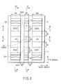
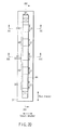
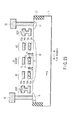
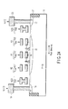
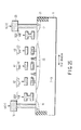
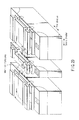
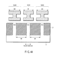
- a semiconductor integrated circuit comprises a semiconductor substrate, an element isolation insulating layer formed in a surface region of the semiconductor substrate, a diffusion layer of a first conductivity type formed in an element region surrounded by the element isolation insulating layer, first and second MIS type devices aligned in a first direction on the diffusion layer, and two select gate transistors arranged at two end portions of the diffusion layer in the first direction, respectively, wherein each of the first and second MIS type devices has a stack gate structure having a floating gate and a control gate electrode, the first MIS type device functions as an aging device, and the second MIS type device functions as a control device which controls an electric charge retention characteristic of the aging device.
- the aging of an aging device is controlled by two control devices which sandwich the aging device, not by the thickness of a tunnel insulating film.
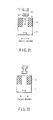
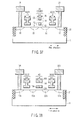
- a width W1 in the second direction of the first element region AA1 is laid out to be smaller than widths W2 and W3 in the second direction of the second and third element regions AA2 and AA3.
- the second MIS type device A2 like the first MIS type device A1, has a stack gate structure. More specifically, on the semiconductor substrate 11, a floating gate (FG) 13A is formed through a tunnel insulating film 12A. On the floating gate 13A, a control gate electrode (CG) 15A is formed through an inter-electrode insulating layer 14A.
- FG floating gate
- CG control gate electrode
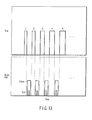
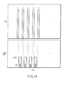
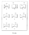
- the select gate transistors SGD1, SGS1, SGD2, SGS2, SGD3, and SGS3, like the first, second, and third MIS type devices A1, A2, and A3, have stack gate structures. However, upper gate electrodes and lower gate electrodes are connected to each other by conductive plugs 999.
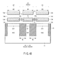
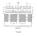
- FIGS. 8 and 9 are obtained by removing the diffusion layers 22 and 22A from FIGS. 6 and 7. In the configurations, predetermined functions of an aging device can be realized.
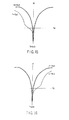
- the rectangular pulses 1, 2, 3, 4, 5, ... in which the magnitudes and the ranges of the write potentials Vcg are constant may be applied to the control gate electrodes 15 and 15A at predetermined intervals.
- the electrons in the floating gate 13 are discharged with elapse of time.
- the channel region of the MIS type device A1 returns from the P-type to the N-type, and the MIS type device A1 is turned off.
- the leakage characteristics are inspected before shipping. According to the result, conditions for a method of writing (injection of electric charges) in the control device can be controlled.
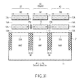
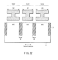
- an element isolation insulating layer 21 having an STI structure is formed in the semiconductor substrate 11.
- An element region (active area) AA is surrounded by the element isolation insulating layer 21.
- the width of the element region (active area) AA in the second direction is set as W1.
- the length of the floating gate 13 in the first direction is set as L1, and the width thereof in the second direction is set as W1.
- a diffusion layer 22 is formed in the semiconductor substrate 11 immediately below the first, second, and third MIS type devices A1, A2, and A3.
- the diffusion layer 22 is of an N-type (N-Well).
- N-Well N-type polysilicon
- the first MIS type device A1 has a stack gate structure. More specifically, on the semiconductor substrate 11, a floating gate (FG) 13 is formed through a tunnel insulating film 12, and a control gate electrode (CG) 15 is formed on the floating gate 13 through an inter-electrode insulating layer 14.
- FG floating gate
- CG control gate electrode
- a diffusion layer 22A is formed in the semiconductor substrate 11 immediately below the second MIS type device A2.
- an aging (life time) of a control device In order to improve controllability of an aging (life time) of an aging device, an aging (life time) of a control device must be longer than the aging of the aging device.
- the first MIS type device A1 has a stack gate structure. More specifically, on the semiconductor substrate 11, a floating gate (FG) 13 is formed through a tunnel insulating film 12, and a control gate electrode (CG) 15 is formed on the floating gate 13 through an inter-electrode insulating layer 14.
- FG floating gate
- CG control gate electrode
- a diffusion layer 22A is formed in the semiconductor substrate 11 immediately below the second MIS type device A2.
Landscapes
- Engineering & Computer Science (AREA)
- Microelectronics & Electronic Packaging (AREA)
- General Physics & Mathematics (AREA)
- Physics & Mathematics (AREA)
- Power Engineering (AREA)
- Ceramic Engineering (AREA)
- Condensed Matter Physics & Semiconductors (AREA)
- Manufacturing & Machinery (AREA)
- Computer Hardware Design (AREA)
- Non-Volatile Memory (AREA)
- Semiconductor Memories (AREA)
- Metal-Oxide And Bipolar Metal-Oxide Semiconductor Integrated Circuits (AREA)
- Semiconductor Integrated Circuits (AREA)
- Read Only Memory (AREA)
Applications Claiming Priority (2)
| Application Number | Priority Date | Filing Date | Title |
|---|---|---|---|
| JP2006257752 | 2006-09-22 | ||
| JP2007186344A JP2008103675A (ja) | 2006-09-22 | 2007-07-17 | 半導体集積回路 |
Publications (3)
| Publication Number | Publication Date |
|---|---|
| EP1903601A2 true EP1903601A2 (de) | 2008-03-26 |
| EP1903601A3 EP1903601A3 (de) | 2008-07-16 |
| EP1903601B1 EP1903601B1 (de) | 2009-08-19 |
Family
ID=38801271
Family Applications (1)
| Application Number | Title | Priority Date | Filing Date |
|---|---|---|---|
| EP07116233A Expired - Fee Related EP1903601B1 (de) | 2006-09-22 | 2007-09-12 | Elektronischer Zeitschalter mit Schwebegattertransistoren und Verfahren zum Initialisieren desselben |
Country Status (4)
| Country | Link |
|---|---|
| US (1) | US7884416B2 (de) |
| EP (1) | EP1903601B1 (de) |
| JP (1) | JP2008103675A (de) |
| DE (1) | DE602007002023D1 (de) |
Families Citing this family (13)
| Publication number | Priority date | Publication date | Assignee | Title |
|---|---|---|---|---|
| JP4212622B2 (ja) | 2006-11-30 | 2009-01-21 | 株式会社東芝 | 時限スイッチ付き情報担体及び半導体集積回路 |
| JP4679528B2 (ja) | 2007-01-30 | 2011-04-27 | 株式会社東芝 | リフレッシュトリガー付き半導体記憶装置 |
| US8247861B2 (en) * | 2007-07-18 | 2012-08-21 | Infineon Technologies Ag | Semiconductor device and method of making same |
| US8320191B2 (en) | 2007-08-30 | 2012-11-27 | Infineon Technologies Ag | Memory cell arrangement, method for controlling a memory cell, memory array and electronic device |
| WO2009059329A1 (en) * | 2007-11-01 | 2009-05-07 | Jonker, Llc | Integrated circuit embedded with non-volatile one-time-programmable and multiple-time programmable memory |
| US8580622B2 (en) * | 2007-11-14 | 2013-11-12 | Invensas Corporation | Method of making integrated circuit embedded with non-volatile programmable memory having variable coupling |
| US7787295B2 (en) * | 2007-11-14 | 2010-08-31 | Jonker Llc | Integrated circuit embedded with non-volatile multiple-time programmable memory having variable coupling |
| US7876615B2 (en) * | 2007-11-14 | 2011-01-25 | Jonker Llc | Method of operating integrated circuit embedded with non-volatile programmable memory having variable coupling related application data |
| JP5221172B2 (ja) * | 2008-02-29 | 2013-06-26 | 株式会社東芝 | Nand混載型半導体時限スイッチ |
| US8305805B2 (en) * | 2008-11-03 | 2012-11-06 | Invensas Corporation | Common drain non-volatile multiple-time programmable memory |
| US8203861B2 (en) | 2008-12-30 | 2012-06-19 | Invensas Corporation | Non-volatile one-time—programmable and multiple-time programmable memory configuration circuit |
| JP2013120815A (ja) * | 2011-12-07 | 2013-06-17 | Sony Corp | Esd保護回路およびこれを備えた半導体装置 |
| US8963647B2 (en) * | 2013-02-20 | 2015-02-24 | Board Of Trustees Of Michigan State University | Self-powered timer apparatus |
Citations (6)
| Publication number | Priority date | Publication date | Assignee | Title |
|---|---|---|---|---|
| US5760644A (en) * | 1995-10-25 | 1998-06-02 | Nvx Corporation | Integrated circuit timer function using natural decay of charge stored in a dielectric |
| JP2004172404A (ja) * | 2002-11-20 | 2004-06-17 | Toshiba Corp | 半導体集積回路 |
| US20040149816A1 (en) * | 2003-01-31 | 2004-08-05 | Yuuki Tomoeda | IC-card service period setting method, IC card, IC card case and battery charger |
| US6856581B1 (en) * | 2000-10-31 | 2005-02-15 | International Business Machines Corporation | Batteryless, oscillatorless, binary time cell usable as an horological device with associated programming methods and devices |
| US20060087360A1 (en) * | 2004-09-28 | 2006-04-27 | Hiroshi Watanabe | Semiconductor device |
| US20060152208A1 (en) * | 2002-07-08 | 2006-07-13 | Kabushiki Kaisha Toshiba | Time limit function utilization apparatus |
Family Cites Families (6)
| Publication number | Priority date | Publication date | Assignee | Title |
|---|---|---|---|---|
| US5361227A (en) * | 1991-12-19 | 1994-11-01 | Kabushiki Kaisha Toshiba | Non-volatile semiconductor memory device and memory system using the same |
| JP4151229B2 (ja) * | 2000-10-26 | 2008-09-17 | ソニー株式会社 | 不揮発性半導体記憶装置およびその製造方法 |
| JP2005285818A (ja) * | 2004-03-26 | 2005-10-13 | Toshiba Corp | 半導体装置およびその製造方法 |
| JP4421364B2 (ja) | 2004-04-16 | 2010-02-24 | 株式会社東芝 | 半導体装置 |
| JP4410188B2 (ja) * | 2004-11-12 | 2010-02-03 | 株式会社東芝 | 半導体記憶装置のデータ書き込み方法 |
| US20070247915A1 (en) * | 2006-04-21 | 2007-10-25 | Intersil Americas Inc. | Multiple time programmable (MTP) PMOS floating gate-based non-volatile memory device for a general-purpose CMOS technology with thick gate oxide |
-
2007
- 2007-07-17 JP JP2007186344A patent/JP2008103675A/ja active Pending
- 2007-09-11 US US11/853,415 patent/US7884416B2/en not_active Expired - Fee Related
- 2007-09-12 DE DE602007002023T patent/DE602007002023D1/de not_active Expired - Fee Related
- 2007-09-12 EP EP07116233A patent/EP1903601B1/de not_active Expired - Fee Related
Patent Citations (6)
| Publication number | Priority date | Publication date | Assignee | Title |
|---|---|---|---|---|
| US5760644A (en) * | 1995-10-25 | 1998-06-02 | Nvx Corporation | Integrated circuit timer function using natural decay of charge stored in a dielectric |
| US6856581B1 (en) * | 2000-10-31 | 2005-02-15 | International Business Machines Corporation | Batteryless, oscillatorless, binary time cell usable as an horological device with associated programming methods and devices |
| US20060152208A1 (en) * | 2002-07-08 | 2006-07-13 | Kabushiki Kaisha Toshiba | Time limit function utilization apparatus |
| JP2004172404A (ja) * | 2002-11-20 | 2004-06-17 | Toshiba Corp | 半導体集積回路 |
| US20040149816A1 (en) * | 2003-01-31 | 2004-08-05 | Yuuki Tomoeda | IC-card service period setting method, IC card, IC card case and battery charger |
| US20060087360A1 (en) * | 2004-09-28 | 2006-04-27 | Hiroshi Watanabe | Semiconductor device |
Also Published As
| Publication number | Publication date |
|---|---|
| US20080074180A1 (en) | 2008-03-27 |
| EP1903601A3 (de) | 2008-07-16 |
| US7884416B2 (en) | 2011-02-08 |
| JP2008103675A (ja) | 2008-05-01 |
| DE602007002023D1 (de) | 2009-10-01 |
| EP1903601B1 (de) | 2009-08-19 |
Similar Documents
| Publication | Publication Date | Title |
|---|---|---|
| EP1903601B1 (de) | Elektronischer Zeitschalter mit Schwebegattertransistoren und Verfahren zum Initialisieren desselben | |
| EP3196884B1 (de) | Schwebegate nichtflüchtige speicherstruktur | |
| US8000139B2 (en) | Multiple time programmable (MTP) PMOS floating gate-based non-volatile memory device for a general purpose CMOS technology with thick gate oxide | |
| US7209392B2 (en) | Single poly non-volatile memory | |
| US10553597B2 (en) | Memory cell including a plurality of wells | |
| US6423584B2 (en) | method for forming capacitors and field effect transistors in a semiconductor integrated circuit device | |
| KR100389130B1 (ko) | 2비트 동작의 2트랜지스터를 구비한 불휘발성 메모리소자 | |
| US8093664B2 (en) | Non-volatile semiconductor memory device and depletion-type MOS transistor | |
| EP0739016A2 (de) | Nichtflüchtige Halbleiterspeicheranordnung mit Block-Löschfunktion | |
| US20070045673A1 (en) | Nonvolatile memory devices and methods of fabricating the same | |
| US7515468B2 (en) | Nonvolatile memory device | |
| US20070120175A1 (en) | Eeprom | |
| US7489005B2 (en) | Eeprom | |
| US7869279B1 (en) | EEPROM memory device and method of programming memory cell having N erase pocket and program and access transistors | |
| US6914826B2 (en) | Flash memory structure and operating method thereof | |
| US20050145922A1 (en) | EEPROM and flash EEPROM | |
| JP3264365B2 (ja) | 不揮発性記憶素子 | |
| US7301219B2 (en) | Electrically erasable programmable read only memory (EEPROM) cell and method for making the same | |
| KR101128715B1 (ko) | 비휘발성 메모리 셀, 그 동작방법 및 그 제조방법 | |
| US7019356B2 (en) | Memory device with reduced cell area | |
| KR102540214B1 (ko) | 싱글 폴리 비휘발성 메모리 소자 및 이를 이용한 제조 방법 | |
| DE FR | Elektronischer Zeitschalter mit Schwebegattertransistoren und Verfahren zum Initialisieren desselben Horloge électronique ayant des transistors à grille flottante et procédé d’initialisation correspondant | |
| JP2021019029A (ja) | 不揮発性半導体記憶装置 | |
| KR20020058460A (ko) | 비휘발성 메모리 소자 | |
| Fox | Development and Characterisation of a Process Technology for a 0.25 µm SiGe: C RF-BiCMOS embedded Flash Memory |
Legal Events
| Date | Code | Title | Description |
|---|---|---|---|
| PUAI | Public reference made under article 153(3) epc to a published international application that has entered the european phase |
Free format text: ORIGINAL CODE: 0009012 |
|
| 17P | Request for examination filed |
Effective date: 20070912 |
|
| AK | Designated contracting states |
Kind code of ref document: A2 Designated state(s): AT BE BG CH CY CZ DE DK EE ES FI FR GB GR HU IE IS IT LI LT LU LV MC MT NL PL PT RO SE SI SK TR |
|
| AX | Request for extension of the european patent |
Extension state: AL BA HR MK YU |
|
| PUAL | Search report despatched |
Free format text: ORIGINAL CODE: 0009013 |
|
| AK | Designated contracting states |
Kind code of ref document: A3 Designated state(s): AT BE BG CH CY CZ DE DK EE ES FI FR GB GR HU IE IS IT LI LT LU LV MC MT NL PL PT RO SE SI SK TR |
|
| AX | Request for extension of the european patent |
Extension state: AL BA HR MK RS |
|
| 17Q | First examination report despatched |
Effective date: 20080910 |
|
| GRAP | Despatch of communication of intention to grant a patent |
Free format text: ORIGINAL CODE: EPIDOSNIGR1 |
|
| AKX | Designation fees paid |
Designated state(s): DE FR GB |
|
| GRAS | Grant fee paid |
Free format text: ORIGINAL CODE: EPIDOSNIGR3 |
|
| GRAA | (expected) grant |
Free format text: ORIGINAL CODE: 0009210 |
|
| AK | Designated contracting states |
Kind code of ref document: B1 Designated state(s): DE FR GB |
|
| REG | Reference to a national code |
Ref country code: GB Ref legal event code: FG4D |
|
| REF | Corresponds to: |
Ref document number: 602007002023 Country of ref document: DE Date of ref document: 20091001 Kind code of ref document: P |
|
| PLBE | No opposition filed within time limit |
Free format text: ORIGINAL CODE: 0009261 |
|
| STAA | Information on the status of an ep patent application or granted ep patent |
Free format text: STATUS: NO OPPOSITION FILED WITHIN TIME LIMIT |
|
| 26N | No opposition filed |
Effective date: 20100520 |
|
| PG25 | Lapsed in a contracting state [announced via postgrant information from national office to epo] |
Ref country code: DE Free format text: LAPSE BECAUSE OF NON-PAYMENT OF DUE FEES Effective date: 20100401 |
|
| GBPC | Gb: european patent ceased through non-payment of renewal fee |
Effective date: 20110912 |
|
| PG25 | Lapsed in a contracting state [announced via postgrant information from national office to epo] |
Ref country code: GB Free format text: LAPSE BECAUSE OF NON-PAYMENT OF DUE FEES Effective date: 20110912 |
|
| REG | Reference to a national code |
Ref country code: FR Ref legal event code: PLFP Year of fee payment: 9 |
|
| PGFP | Annual fee paid to national office [announced via postgrant information from national office to epo] |
Ref country code: FR Payment date: 20150629 Year of fee payment: 9 |
|
| REG | Reference to a national code |
Ref country code: FR Ref legal event code: ST Effective date: 20170531 |
|
| PG25 | Lapsed in a contracting state [announced via postgrant information from national office to epo] |
Ref country code: FR Free format text: LAPSE BECAUSE OF NON-PAYMENT OF DUE FEES Effective date: 20160930 |