EP1903594A2 - Teilchenstrahlinstrument und Verfahren zur Detektion geladener Teilchen - Google Patents
Teilchenstrahlinstrument und Verfahren zur Detektion geladener Teilchen Download PDFInfo
- Publication number
- EP1903594A2 EP1903594A2 EP07253731A EP07253731A EP1903594A2 EP 1903594 A2 EP1903594 A2 EP 1903594A2 EP 07253731 A EP07253731 A EP 07253731A EP 07253731 A EP07253731 A EP 07253731A EP 1903594 A2 EP1903594 A2 EP 1903594A2
- Authority
- EP
- European Patent Office
- Prior art keywords
- sample
- charged particles
- detector
- secondary charged
- column
- Prior art date
- Legal status (The legal status is an assumption and is not a legal conclusion. Google has not performed a legal analysis and makes no representation as to the accuracy of the status listed.)
- Withdrawn
Links
- 239000002245 particle Substances 0.000 title claims abstract description 133
- 238000000034 method Methods 0.000 title claims description 11
- 230000005684 electric field Effects 0.000 claims abstract description 48
- 230000003287 optical effect Effects 0.000 claims abstract description 22
- 230000004907 flux Effects 0.000 description 5
- 230000007423 decrease Effects 0.000 description 4
- 230000000694 effects Effects 0.000 description 4
- 238000010276 construction Methods 0.000 description 3
- 125000003821 2-(trimethylsilyl)ethoxymethyl group Chemical group [H]C([H])([H])[Si](C([H])([H])[H])(C([H])([H])[H])C([H])([H])C(OC([H])([H])[*])([H])[H] 0.000 description 2
- 230000001133 acceleration Effects 0.000 description 2
- 201000009310 astigmatism Diseases 0.000 description 2
- 230000003247 decreasing effect Effects 0.000 description 2
- 238000001514 detection method Methods 0.000 description 2
- 238000010894 electron beam technology Methods 0.000 description 2
- 230000005686 electrostatic field Effects 0.000 description 2
- 238000013178 mathematical model Methods 0.000 description 2
- 238000004626 scanning electron microscopy Methods 0.000 description 2
- 230000004075 alteration Effects 0.000 description 1
- 230000000284 resting effect Effects 0.000 description 1
Images




Classifications
-
- H—ELECTRICITY
- H01—ELECTRIC ELEMENTS
- H01J—ELECTRIC DISCHARGE TUBES OR DISCHARGE LAMPS
- H01J37/00—Discharge tubes with provision for introducing objects or material to be exposed to the discharge, e.g. for the purpose of examination or processing thereof
- H01J37/02—Details
-
- H—ELECTRICITY
- H01—ELECTRIC ELEMENTS
- H01J—ELECTRIC DISCHARGE TUBES OR DISCHARGE LAMPS
- H01J37/00—Discharge tubes with provision for introducing objects or material to be exposed to the discharge, e.g. for the purpose of examination or processing thereof
- H01J37/02—Details
- H01J37/244—Detectors; Associated components or circuits therefor
-
- H—ELECTRICITY
- H01—ELECTRIC ELEMENTS
- H01J—ELECTRIC DISCHARGE TUBES OR DISCHARGE LAMPS
- H01J37/00—Discharge tubes with provision for introducing objects or material to be exposed to the discharge, e.g. for the purpose of examination or processing thereof
- H01J37/26—Electron or ion microscopes; Electron or ion diffraction tubes
- H01J37/261—Details
-
- H—ELECTRICITY
- H01—ELECTRIC ELEMENTS
- H01J—ELECTRIC DISCHARGE TUBES OR DISCHARGE LAMPS
- H01J37/00—Discharge tubes with provision for introducing objects or material to be exposed to the discharge, e.g. for the purpose of examination or processing thereof
- H01J37/26—Electron or ion microscopes; Electron or ion diffraction tubes
- H01J37/28—Electron or ion microscopes; Electron or ion diffraction tubes with scanning beams
-
- H—ELECTRICITY
- H01—ELECTRIC ELEMENTS
- H01J—ELECTRIC DISCHARGE TUBES OR DISCHARGE LAMPS
- H01J2237/00—Discharge tubes exposing object to beam, e.g. for analysis treatment, etching, imaging
- H01J2237/244—Detection characterized by the detecting means
- H01J2237/2444—Electron Multiplier
-
- H—ELECTRICITY
- H01—ELECTRIC ELEMENTS
- H01J—ELECTRIC DISCHARGE TUBES OR DISCHARGE LAMPS
- H01J2237/00—Discharge tubes exposing object to beam, e.g. for analysis treatment, etching, imaging
- H01J2237/244—Detection characterized by the detecting means
- H01J2237/2448—Secondary particle detectors
-
- H—ELECTRICITY
- H01—ELECTRIC ELEMENTS
- H01J—ELECTRIC DISCHARGE TUBES OR DISCHARGE LAMPS
- H01J2237/00—Discharge tubes exposing object to beam, e.g. for analysis treatment, etching, imaging
- H01J2237/244—Detection characterized by the detecting means
- H01J2237/2449—Detector devices with moving charges in electric or magnetic fields
Definitions
- This invention relates to a charged particle beam instrument, in particular a scanning electron microscope (SEM), and to a method of detecting charged particles released from a sample in such an instrument.
- SEM scanning electron microscope
- a known scanning electron microscope comprises an electron optical column, a voltage source, an Everhart-Thornley detector and a sample holder, the column being operable to direct a beam of primary electrons at a sample on the sample holder to cause secondary electrons to be released from the sample, the voltage source being operable to establish in the vicinity of the sample an electric field that has a component that draws the secondary electrons towards the detector, and the detector being operable to detect some of the secondary electrons.
- spot size is the diameter of the beam of primary electrons at the surface of the sample
- Working distance is the distance from the sample to an end of an objective lens of the column nearer to the sample
- the semi angle is an angle included by a tip of a cone formed as the beam of primary electrons is focused at the surface of the sample. The SEM is therefore typically used at short working distances.
- the number of secondary electrons that are detected by the detector also decreases at short working distances because the secondary electrons are shielded from the electric field by the sample holder and a pole piece of the objective lens of the column.
- a charged particle beam instrument comprising a charged particle optical column, a voltage source, a detector and a sample holder, the column being operable to direct a beam of primary charged particles at a sample on the sample holder to cause secondary charged particles to be released from the sample, the voltage source being operable to establish in the vicinity of the sample an electric field that has a component that draws the secondary charged particles towards the detector, and the detector being operable to detect secondary charged particles, wherein the instrument further comprises a further voltage source variable between a first voltage that establishes a component of the electric field that draws the secondary charged particles away from the sample, so as to prevent at least some of them from colliding with the sample or sample holder, and a second voltage that establishes a component of the electric field that draws the secondary charged particles towards the sample, so as to prevent at least some of them from colliding with the column, thereby increasing the number of secondary charged particles detected by the detector.
- the invention can provide a charged particle beam instrument that is capable of detecting more of the secondary charged particles than the known instrument, because at least some of the secondary charged particles, which would otherwise collide with the sample, sample holder or column before being detected by the detector, are prevented from so colliding by the component of the electric field established by the further voltage source.
- the further voltage source would be operated at the first voltage when the behaviour of the secondary charged particles is determined predominantly by a magnetic field of an objective lens of the column, so as to prevent at least some of the secondary charged particles from colliding with the sample or the sample holder, and would be operated at the second voltage when the behaviour of the secondary charged particles is determined predominantly by the electric field, so as to prevent at least some of the secondary charged particles from colliding with the column.
- the charged particle optical column is preferably an electron optical column.
- the charged particle beam instrument is a scanning electron microscope (SEM) of which the charged particle optical column is an electron optical column operable to direct a beam of primary electrons at the sample to cause secondary electrons to be released from the sample.
- SEM scanning electron microscope
- the detector may advantageously be operable to detect some of the secondary charged particles by responding to photons that collide with it, the photons being generated as a result of collisions between some of the secondary charged particles and gas molecules between the sample holder and the detector.
- the detector may advantageously be operable to detect some of the secondary charged particles by responding to those of the secondary charged particles that collide with it.
- the voltage source may advantageously form part of the detector.
- the detector is located outside the electron optical column at the side of a pole piece of an objective lens of the column.
- the detector is an Everhart-Thornley detector.
- the further voltage source is preferably continuously variable between the first and second voltages.
- the secondary charged particles are released at a wide range of angles to the surface of the sample, from nearly parallel to perpendicular to the surface.
- a component of the electric field of a magnitude that prevents some of the secondary charged particles released at an angle of, say, 60° to the surface of the sample from colliding with the column may cause secondary charged particles released at an angle of, say, 30° to the surface of the sample to collide with the sample or sample holder.
- a component of the electric field of a magnitude that prevents some of the secondary charged particles released at an angle of 30° to the surface of the sample from colliding with the column without causing them to collide with the sample may not prevent the secondary charged particles released at an angle of 60° to the surface of the sample from colliding with the column.
- a user of the instrument can set the voltage of the further voltage source so as to establish a component of the electric field that prevents at least some of the secondary charged particles released at a particular angle or range of angles to the surface of the sample from colliding with the sample, sample holder or column.
- the user would set the voltage of the further voltage source so as to establish a component of the electric field that prevents at least some of the secondary charged particles released at an angle or range of angles to the surface of the sample at which the largest number of secondary charged particles are released from the sample from colliding with the sample, sample holder or column. It is believed that the greatest increase in the number of secondary charged particles detected by the detector can be obtained in this way.
- the user could set the voltage of the further voltage source so as to establish a component of the electric field that enables at least some of the secondary charged particles released at an angle or range of angles to the surface of the sample that would otherwise cause them to collide with the sample, sample holder or column to be detected by the detector. It is believed that information relating to the sample that can not be obtained using the known instrument can be obtained in this way.
- the instrument may advantageously include a controller operable to vary the voltage of the further voltage source between the first and second voltages so as to maximise an output of the detector.
- the column includes magnetic coils for generating a magnetic field inside the column to focus and scan the beam of primary charged particles relative to the surface of the sample. Leakage of magnetic flux from the objective lens of the column causes the magnetic field to extend outside the objective lens of the column in the vicinity of the sample. The magnetic field causes the secondary charged particles to describe spirals.
- the strength of the magnetic field required to focus and scan the beam of primary charged particles depends on the kinetic energy of the charged particles that constitute the beam. For a beam of primary charged particles with a relatively high kinetic energy, a relatively strong magnetic field is required, whereas for a beam of primary charged particles with a relatively low kinetic energy, a relatively weak magnetic field is required. The strength of the magnetic field in the vicinity of the sample thus depends on the kinetic energy of the primary charged particles.
- the diameter of the spiral described by the charged particle is inversely proportional to the strength of the magnetic field.
- the magnetic field in the vicinity of the sample is relatively strong and the secondary charged particles describe spirals of relatively small diameter.
- a secondary charged particle that is released from the sample at a small angle to the surface of the sample into a relatively strong magnetic field may spiral into the sample or sample holder.
- Such a secondary charged particle can be prevented from spiralling into the sample or sample holder by a component of the electric field that draws the secondary charged particle away from the sample.
- the primary charged particles have a relatively low kinetic energy
- the magnetic field in the vicinity of the sample is relatively weak and the secondary charged particles describe spirals of relatively large diameter.
- a secondary charged particle that is released from the sample at a large angle to the surface of the sample into a relatively weak magnetic field may spiral into the column.
- Such a secondary charged particle can be prevented from spiralling into the column by a component of the electric field that draws the secondary charged particle towards the sample.
- the further voltage source can therefore be used to prevent at least some of the secondary charged particles from colliding with the sample, sample holder or column both with a beam constituted by primary charged particles with a relatively low kinetic energy and with a beam constituted by primary charged particles with a relatively high kinetic energy.
- the further voltage source can prevent at least some of the secondary charged particles from colliding with the sample, sample holder or column for a wide variety of conditions of kinetic energy of the primary charged particles, kinetic energy of the secondary charged particles and angle to the surface of the sample at which the secondary charged particles are released.
- the further voltage source is variable over a range of 50V.
- the further voltage source may advantageously be connected to an electrode located between the objective lens of the column and the sample holder.
- the electrode may advantageously be formed with an aperture and be located relative to the objective lens such that the beam of primary charged particles may be directed through the electrode at the sample.
- the aperture is substantially circular and the electrode is located relative to the objective lens such that the optical axis of the column passes through the centre of the aperture.
- This configuration of the electrode is advantageous because the components of the electric field due to the electrode are substantially symmetrical about the optical axis of the column.
- the components of the electric field due to the electrode therefore do not cause astigmatism of the beam of primary charged particles (astigmatism is a deformation of the beam that causes the beam to be non-circular at the sample), which might otherwise be expected to result from an electrode located between the column and the sample, particularly in the case of a beam of charged particles with a relatively low kinetic energy.
- the further voltage source may advantageously be connected to the objective lens of the column and/or the sample holder.
- the further voltage source could be connected to both the objective lens and the sample holder, typically it would be connected to one or the other.
- the sample holder would typically be connected to electrical ground
- the further voltage source is connected to the sample holder
- the objective lens would typically be connected to electrical ground
- the further voltage source is connected to the sample holder, the objective lens is connected to electrical ground, and the further voltage source is variable between +25V and -25V.
- a method of detecting charged particles comprising the steps of directing a beam of primary charged particles from a charged particle optical column at a sample to cause secondary charged particles to be released from the sample, establishing in the vicinity of the sample an electric field that has a component that draws the secondary charged particles towards a detector, and detecting at least some of the secondary charged particles by means of the detector, wherein the method further comprises the step of increasing the number of secondary charged particles detected by the detector by establishing a component of the electric field that draws the secondary charged particles away from the sample, so as to prevent at least some of them from colliding with the sample, or that draws the secondary charged particles towards the sample, so as to prevent at least some of them from colliding with the column.
- the step of establishing the component of the electric field that draws the secondary charged particles away from or towards the sample may advantageously comprise establishing a component of the electric field that draws the secondary charged particles away from the sample where the behaviour of the secondary charged particles is determined predominantly by a magnetic field of an objective lens of the column, and establishing a component of the electric field that draws the secondary charged particles towards the sample where the behaviour of the secondary charged particles is determined predominantly by the electric field.
- the step of establishing the component of the electric field that draws the secondary charged particles away from or towards the sample may advantageously comprise determining the magnitude and direction of the component according to an angle or range of angles to the surface of the sample at which at least some of the secondary charged particles are released, to a kinetic energy of the primary charged particles of the beam and/or to a kinetic energy or range of kinetic energies of the secondary charged particles.
- Figure 1 shows a portion 2 of a Carl Zeiss EVO scanning electron microscope (SEM).
- the portion 2 includes a pole piece 3 of an objective lens of an electron optical column 4, a sample 5 resting on a sample holder 6, and an accelerating electrode 7 of an Everhart-Thornley secondary electron detector 8.
- the detector 8 is located outside the column 4 and to the side of the pole piece 3 of the objective lens of the column 4.
- n emitted SE ⁇ E ⁇ ⁇ ⁇ ⁇ d n d ⁇ ⁇ d n d E ⁇ ⁇ d ⁇ ⁇ d E ⁇ .
- the distance from the centre of the aperture of the pole piece 3 of the objective lens of the column 4 to the centre of the end of the accelerating electrode 7 is about 19mm.
- Table 2 sets out the total number of secondary electrons detected by the detector 8 with voltages of 0, -5, -10, -15 and -20V applied to the sample holder 6.
- the model assumes a beam energy (i.e. kinetic energy of the primary electrons) of 30keV, a kinetic energy of the secondary electrons of 2eV, a magnetic field of the objective lens of the column corresponding to that which would focus a beam starting at 246mm from an end of the pole piece nearer to the sample, a voltage of +400V applied to the accelerating electrode 7 of the detector 8 and the pole piece 3 of the objective lens of the column connected to electrical ground.
- a beam energy i.e. kinetic energy of the primary electrons
- the last row but one of the table gives the percentage detection efficiency of the detector, for each of the voltages applied to the sample holder, calculated from the total number of secondary electrons emitted from the sample, while the last row of the table gives the percentage improvement in detection efficiency of the detector for each of the voltages applied to the sample holder when compared with a voltage of 0V applied to the sample holder.
- the effect of Lambert's cosine law is already included in the number of emitted secondary electrons and hence in the number of detected secondary electrons.
- Table 3 sets out the total number of secondary electrons detected by the detector and percentage efficiency and improvement in efficiency of the detector under the same conditions as in table 2 above but assuming a kinetic energy of the secondary electrons of 3eV.
- Table 3 SAMPLE BIAS: 0V -5V -10V -15V -20V ⁇ [in°] NUMBER DETECTED SE NUMBER DETECTED SE NUMBER DETECTED SE NUMBER DETECTED SE NUMBER DETECTED SE 90 0 0 0 0 0 85 0 0 0 0 0 80 0 0 0 0 0 75 0 0 0 0 0 0 70 0 0 0 0 0 0 65 0 0 0 0 0 0 60 0 0 0 0 0 0 0 0 55 0 0 0 0.93 0 50 0 0 0.26 0.43 0 45 0 0.96 0 0 1.13 40 0 0 1.26 0.59 0 35
- Table 4 sets out the total number of secondary electrons detected by the detector and percentage efficiency and improvement in efficiency under the same conditions as in tables 2 and 3 above but assuming a kinetic energy of the secondary electrons of 4eV.
- Table 4 SAMPLE BIAS: 0V -5V -10V -15V -20V ⁇ [in°] NUMBER OF DETECTED SE NUMBER OF DETECTED SE NUMBER OF DETECTED SE NUMBER OF DETECTED SE NUMBER OF DETECTED SE 90 0 0 0 0 0 85 0 0 0 0 0 80 0 0 0 0 0 75 0 0 0 0 0 0 70 0 0 0 0 0 0 65 0 0 0 0 0 0 60 0 0 0 0 0 0 50 0 0 0 0 0 1.30 45 0 0 1.30 0.96 0 40 0 0 0 1.18 1.18 35 0 0 0 0 1.18
- Table 5 sets out the total number of secondary electrons detected by the detector and percentage efficiency and improvement in efficiency (if any) under the same conditions as in tables 2 to 4 above but assuming a kinetic energy of the secondary electrons of 5eV.
- Table 5 SAMPLE BIAS: 0V -5V -10V -15V -20V ⁇ [in°] NUMBER OF DETECTED SE NUMBER OF DETECTED SE NUMBER OF DETECTED SE NUMBER OF DETECTED SE NUMBER OF DETECTED SE 90 0 0 0 0 0 85 0 0 0 0 0 80 0 0 0 0 0 75 0 0 0 0 0 0 70 0 0 0 0 0 65 0 0 0 0 0 0 60 0 0 0 0 0 0 0.51 50 0 0 1.13 0 0 45 0 0 0 0 1.22 1.22 40 0 0 0 0 0 1.01 35 0.79 0.87
- Table 6 sets out the total number of secondary electrons detected by the detector and percentage efficiency and improvement in efficiency of the detector with voltages of 0, +1, +2, +3 and +4V applied to the sample holder 6.
- the model assumes a beam energy of 1keV, and a kinetic energy of the secondary electrons of 3eV.
- the magnetic field of the objective lens, voltage applied to the detector and grounding of the sample holder are the same as previously.
- the mathematical model predicts that an SEM in accordance with the first aspect of the invention can detect nearly 57% more secondary electrons (3eV) than the known instrument when used with a high energy primary electron beam (where the behaviour of the secondary electrons is predominantly determined by the magnetic field of the objective lens).
- Table 6 shows that the SEM of the invention can also detect nearly 50% more secondary electrons (3eV) than the known instrument when used with a low energy primary electron beam (where the behaviour of the secondary electrons is predominantly determined by the component of the electric field due to the accelerating electrode of the detector).
- FIG. 1 shows a portion 10 of a first charged particle beam instrument in accordance with the first aspect of the invention in the form of an SEM.
- the portion 10 includes a charged particle optical column in the form of an electron optical column 12, a detector in the form of an Everhart-Thornley detector 14 and a further voltage source 16 connected to an annular electrode 17 located between a pole piece 22 of an objective lens of the electron optical column 12 and a sample holder 18 on which a sample 20 rests, the annular electrode 17 being located above the sample 20, such that a beam of primary electrons (not shown) can be directed through the annular electrode 17 at the sample 20.
- the column 12 also includes magnetic coils (not shown) for generating a magnetic field that focuses and scans the beam of primary electrons relative to the sample 20.
- the Everhart-Thornley detector 14 includes an accelerating electrode 24 connected to a voltage source (not shown).
- a +400V voltage applied to the accelerating electrode 24 by the voltage source gives rise to an electric field between the sample holder 18 and the pole piece 22, which field has a component that causes secondary electrons released from the sample 20 to be drawn towards the detector 14.
- the further voltage source 16 comprises +25V and -25V voltage supplies and a voltage divider connected between the voltage supplies, the voltage divider being operable to produce an output voltage in the range +/-25V.
- the output of the voltage divider is connected to the annular electrode 17.
- the pole piece 22 is connected to electrical ground.
- Figure 2 shows a portion 10 of a second SEM in accordance with the first aspect of the invention, the second SEM being identical with the first SEM except that the annular electrode is not present and the output of the voltage divider of the further voltage source 16 is connected to the sample holder 18.
- components common to the first and second SEMs are denoted by the same reference numerals.
- Figure 3 shows a portion 30 of a known SEM of similar construction to the SEM of Figure 2, but without the further voltage source 16.
- the portion 30 includes a column 32, an Everhart-Thornley detector 34 and a sample holder 38 on which a sample 40 rests.
- the SEM of Figure 3 is in use with a beam of primary electrons (not shown) from the column 32 directed at the sample 40.
- the primary electrons have a kinetic energy of approximately 1keV.
- secondary electrons are released from the sample at all angles to the surface of the sample as a result of the beam of primary electrons being directed at the sample. For the purpose of clarity, however, only those secondary electrons released at an angle of 60° to the surface of the sample are shown in Figure 3, denoted generally by reference numeral 42.
- the path 44 described by the electron has components in each of three mutually perpendicular directions.
- the first direction (the x-direction) is parallel to the surface of the sample 40 and parallel to the plane of Figure 4.
- the second direction (the y-direction) is parallel to the surface of the sample and perpendicular to the plane of Figure 4.
- the third direction (the z-direction) is perpendicular to the surface of the sample and parallel to the plane of Figure 4.
- motion from left to right of the drawing figures is considered to be in the positive x-direction
- motion into the plane of the drawing figures is considered to be in the positive y-direction
- motion from top to bottom of the drawing figures is considered to be in the positive z-direction.
- the path 44 of the electron consists of first, intermediate and final portions 46, 48 and 50, respectively.
- first portion 46 the electron is released from the surface of the sample and travels away from the sample 40 in the general direction of the pole piece 33, through the magnetic field. Motion of the electron through the magnetic field causes it to describe a spiral.
- the first portion 46 of the path 44 therefore consists of a portion of a spiral that has components in the positive x- and negative y-directions and in the negative z-direction.
- the spiral is of relatively large but decreasing diameter as the electron travels from the relatively weak region of the magnetic field in the immediate vicinity of the sample 40 into the relatively strong region of the magnetic field in the immediate vicinity of the pole piece 33.
- the magnitude of the component of the spiral in the positive x-direction is increased by the component of the electric field resulting from the voltage applied to the accelerating electrode 35 of the detector 34.
- the electron travels through the relatively strong region of the magnetic field, which causes it to describe a portion of a spiral of relatively small diameter, so that the path of the electron has a component in the negative z-direction at the beginning of the intermediate portion 46 and a component in the positive z-direction at the end of the intermediate portion. Throughout the intermediate portion, the path of the electron has a component in the negative y-direction.
- the final portion 50 of the path 44 consists of a portion of a spiral that has components in the negative y- and positive z-directions.
- the path has a component in the negative x-direction but has a component in the positive x-direction by the end of the final portion because of the component of the electric field established by the accelerating electrode of the detector.
- the portion of the spiral is of relatively large and increasing diameter as the electron travels out of the relatively strong region of the magnetic field into the relatively weak region.
- the electron collides with the sample 40 at a point on the surface of the sample a small distance in the positive x-direction and negative y-direction from the point from which the electron was released at the beginning of the initial portion 46. The electron is therefore not detected by the detector 34.
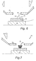
- FIG 5 shows the SEM of Figure 2 in use under similar conditions to the known SEM of Figures 3 and 4, namely with a beam constituted by primary electrons with a kinetic energy of approximately 1keV.
- a voltage of +2V has been applied to the sample holder 18 of the SEM by the further voltage source 16.
- Some of the secondary electrons released at an angle of 60° to the surface of the sample, the electrons being denoted generally by reference numeral 52, are prevented by the resulting component of the electric field from colliding with the sample or the pole piece 22 of the objective lens of the column 12, and therefore reach the detector 14.
- the path 54 of the electron consists of first, intermediate and final portions 56, 58 and 60, respectively.
- the first portion 56 consists of a portion of a spiral that has components in the positive x- and negative y-directions and in the negative z-direction.
- the magnitude of the component in the negative z-direction is reduced, compared with that of the electron shown in Figure 4, by the component of the electric field resulting from the +2V voltage applied to the sample holder 18.
- the electron is moving more slowly than the electron shown in Figure 4, and the diameter of the spiral described by the electron is smaller than that described by the electron shown in Figure 4, because, for a particular strength of magnetic field the diameter of the spiral described by the electron is proportional to its speed.
- the path of the electron has a relatively large component in the negative y-direction and a relatively small component in the positive z-direction.
- the electron describes a portion of a spiral of relatively large and increasing diameter as it travels out of the relatively strong region of the magnetic field.
- the component in the negative y-direction remains greater than the component in the positive z-direction so that when the electron reaches the plane of the surface of the sample, it has travelled sufficiently far in the negative y-direction to avoid colliding with the surface of the sample.
- the effect of the magnetic field decreases and the diameter of the portion of the spiral increases.
- the component of the electric field due to the accelerating electrode of the detector causes the electron to be drawn in the positive x-direction until at the end of the final portion 60 it reaches the detector 14.
- Figure 7 shows the paths of secondary electrons released from the sample 40 in the known SEM at an angle of 45° to the surface of the sample by a beam constituted by primary electrons with a kinetic energy of approximately 30keV.
- the paths of the secondary electrons are denoted generally by reference numeral 62 and it can be seen that in the known SEM, none of the secondary electrons released at an angle of 45° to the surface of the sample reaches the detector, but all instead collide with the sample.
- the path 64 consists of first, intermediate and final portions 66, 68 and 70, respectively.
- the electron is released from the surface of the sample and travels away from the sample 40 in the general direction of the pole piece 33, through the magnetic field in the immediate vicinity of the sample 40.
- the strength of the magnetic field in the immediate vicinity of the sample is less than that of the magnetic field in the immediate vicinity of the pole piece 33, the strength of the magnetic field in the immediate vicinity of the sample is relatively high in comparison with the strength of the magnetic field when the SEM is used with a beam constituted by primary electrons with a kinetic energy of approximately 1keV.
- the electron describes a portion of a spiral with a relatively small diameter.
- the portion of the spiral has components in the positive x- and negative y-directions, and a component in the negative z-direction.
- the electron changes direction so that the path of the electron has a component in the positive x-direction at the beginning of the intermediate portion and a component in the negative x-direction at the end of the intermediate portion.
- the final portion 70 of the path 64 consists of a portion of a spiral that has components in the negative y- and x-directions and positive z-direction.
- the electron collides with the sample 40 at a point on the surface of the sample a small distance in the negative x- and y-directions from the point from which the electron was released at the beginning of the initial portion 66. The electron is not detected by the detector 34.
- Figure 9 shows the SEM of Figure 2 in use under similar conditions to the known SEM of Figures 7 and 8, namely with a beam constituted by primary electrons with a kinetic energy of approximately 30keV. Only those secondary electrons released from the sample at an angle of 45° to the surface of the sample are shown in Figure 9. However, in Figure 9 a voltage of-20V has been applied to the sample holder 18 by the further voltage source 16. Some of the secondary electrons released at an angle of 45° to the surface of the sample, the electrons being denoted generally by reference numeral 72, are prevented by the resulting component of the electric field from colliding with the sample or the pole piece 22 of the objective lens of the column 12, and therefore reach the detector 14.
- the path 74 of the electron consists of first, intermediate and final portions 76, 78 and 80, respectively.
- the first portion 76 consists of a spiral that has components, at various times, in both the positive and negative x- and y-directions, but only in the negative z-direction as the electron travels away from the sample towards the pole piece 22 of the column.
- the diameter of the spiral decreases from the beginning to the end of the first portion 76 as the electron travels from the relatively weak region to the relatively strong region of the magnetic field.
- the electron At the end of the initial portion 76 of the path 74 the electron has almost entered the aperture of the pole piece where it is subjected to a strong magnetic field due to the primary electrons that constitute the beam.
- the magnetic field changes the component of the path of the electron in the negative z-direction to a component in the positive z-direction.
- the electron describes a portion of a spiral of increasing diameter as it travels away from the pole piece 22 towards the sample 20 and from the relatively strong to the relatively weak region of the magnetic field.
- the component of the path of the electron in the positive x-direction increases due to the component of the electric field established by the voltage applied to the accelerating electrode of the detector 14.
- the path of the electron has components in the positive z- and x-directions and is in the immediate vicinity of the sample.
- the component of the electric field in the immediate vicinity of the sample due to the -20V voltage applied to the sample holder 18 changes the component of the path of the electron in the positive z-direction to a component in the negative z-direction.
- the electron travels a sufficient distance in the positive x-direction from the point at which it was released from the surface of the sample at the beginning of the initial portion 76 that the effect of the component of the electric field due to the accelerating electrode of the detector is much greater than that of the magnetic field.
- the final portion 80 of the path 74 is therefore substantially linear in the positive x- and z-directions and at the end of the final portion the electron reaches the detector 14 and is detected.
Landscapes
- Chemical & Material Sciences (AREA)
- Analytical Chemistry (AREA)
- Analysing Materials By The Use Of Radiation (AREA)
Applications Claiming Priority (1)
| Application Number | Priority Date | Filing Date | Title |
|---|---|---|---|
| GB0618770A GB2442027B (en) | 2006-09-23 | 2006-09-23 | Charged particle beam instrument and method of detecting charged particles |
Publications (2)
| Publication Number | Publication Date |
|---|---|
| EP1903594A2 true EP1903594A2 (de) | 2008-03-26 |
| EP1903594A3 EP1903594A3 (de) | 2010-03-31 |
Family
ID=37421506
Family Applications (1)
| Application Number | Title | Priority Date | Filing Date |
|---|---|---|---|
| EP07253731A Withdrawn EP1903594A3 (de) | 2006-09-23 | 2007-09-20 | Teilchenstrahlinstrument und Verfahren zur Detektion geladener Teilchen |
Country Status (4)
| Country | Link |
|---|---|
| US (1) | US7777195B2 (de) |
| EP (1) | EP1903594A3 (de) |
| JP (1) | JP5247099B2 (de) |
| GB (1) | GB2442027B (de) |
Families Citing this family (3)
| Publication number | Priority date | Publication date | Assignee | Title |
|---|---|---|---|---|
| WO2011055521A1 (ja) * | 2009-11-06 | 2011-05-12 | 株式会社日立ハイテクノロジーズ | 荷電粒子顕微鏡 |
| US11087956B2 (en) * | 2018-06-29 | 2021-08-10 | Taiwan Semiconductor Manufacturing Co., Ltd. | Detection systems in semiconductor metrology tools |
| CN108748975B (zh) * | 2018-07-17 | 2024-10-25 | 中南大学 | 一种纳米级高精度增材制造设备 |
Citations (2)
| Publication number | Priority date | Publication date | Assignee | Title |
|---|---|---|---|---|
| US4011450A (en) * | 1974-07-17 | 1977-03-08 | Nihon Denshi Kabushiki Kaisha | Scanning electron device |
| US20020109089A1 (en) * | 2000-10-31 | 2002-08-15 | Krans Jan Martijn | SEM provided with an adjustable final electrode in the electrostatic objective |
Family Cites Families (12)
| Publication number | Priority date | Publication date | Assignee | Title |
|---|---|---|---|---|
| AU521225B2 (en) * | 1977-04-19 | 1982-03-25 | Delalande S.A. | Alkylenedioxy phenyl derivatives |
| JPH01220352A (ja) * | 1988-02-26 | 1989-09-04 | Hitachi Ltd | 走査電子顕微鏡及びその類似装置 |
| US6201240B1 (en) | 1998-11-04 | 2001-03-13 | Applied Materials, Inc. | SEM image enhancement using narrow band detection and color assignment |
| DE69901787T2 (de) * | 1999-03-31 | 2002-11-21 | Advantest Corp., Tokio/Tokyo | Verfahren und Vorrichtung zur Abbildung eines Oberflächenpotentials |
| EP1100112A1 (de) * | 1999-11-12 | 2001-05-16 | Advantest Corporation | Spektrometerobjektiv für ein Teilchenstrahlenergie-Mess-System |
| WO2001041180A1 (de) | 1999-11-29 | 2001-06-07 | Leo Elektronenmikroskopie Gmbh | Detektor für ein rasterelektronenmikroskop mit variablem druck und rasterelektronenmikroskop mit einem solchen detektor |
| JP4073149B2 (ja) | 2000-05-26 | 2008-04-09 | 株式会社日立製作所 | 電子線装置 |
| CZ302126B6 (cs) * | 2000-07-07 | 2010-11-03 | Leo Elektronenmikroskopie Gmbh | Detektor pro prístroje vyzarující korpuskulární zárení, prístroj vyzarující korpuskulární zárení a zpusob detekování existence produktu vzájemného pusobení v tomto prístroji |
| JP2002289129A (ja) | 2001-03-26 | 2002-10-04 | Jeol Ltd | 低真空走査電子顕微鏡 |
| EP1489641B1 (de) * | 2003-06-18 | 2019-08-14 | ICT Integrated Circuit Testing Gesellschaft für Halbleiterprüftechnik mbH | Ablenksystem für geladene Teilchen |
| JP4291109B2 (ja) * | 2003-10-28 | 2009-07-08 | エスアイアイ・ナノテクノロジー株式会社 | 複合型荷電粒子ビーム装置 |
| JP4292068B2 (ja) * | 2003-12-11 | 2009-07-08 | 株式会社日立ハイテクノロジーズ | 走査電子顕微鏡 |
-
2006
- 2006-09-23 GB GB0618770A patent/GB2442027B/en active Active
-
2007
- 2007-09-19 US US11/857,813 patent/US7777195B2/en active Active
- 2007-09-20 EP EP07253731A patent/EP1903594A3/de not_active Withdrawn
- 2007-09-21 JP JP2007245976A patent/JP5247099B2/ja active Active
Patent Citations (2)
| Publication number | Priority date | Publication date | Assignee | Title |
|---|---|---|---|---|
| US4011450A (en) * | 1974-07-17 | 1977-03-08 | Nihon Denshi Kabushiki Kaisha | Scanning electron device |
| US20020109089A1 (en) * | 2000-10-31 | 2002-08-15 | Krans Jan Martijn | SEM provided with an adjustable final electrode in the electrostatic objective |
Also Published As
| Publication number | Publication date |
|---|---|
| US20080078934A1 (en) | 2008-04-03 |
| US7777195B2 (en) | 2010-08-17 |
| JP2008078142A (ja) | 2008-04-03 |
| GB0618770D0 (en) | 2006-11-01 |
| JP5247099B2 (ja) | 2013-07-24 |
| GB2442027B (en) | 2009-08-26 |
| GB2442027A (en) | 2008-03-26 |
| EP1903594A3 (de) | 2010-03-31 |
Similar Documents
| Publication | Publication Date | Title |
|---|---|---|
| JP3268583B2 (ja) | 粒子線装置 | |
| EP1045425B1 (de) | Teilchenstrahlapparat mit Kompensation der chromatischen Aberration | |
| US9997326B2 (en) | Charged particle beam device | |
| US7199365B2 (en) | Electron beam apparatus with aberration corrector | |
| US8618480B2 (en) | Charged particle beam apparatus | |
| JPH0624106B2 (ja) | 粒子線装置の静電磁気複合レンズ | |
| US8314404B2 (en) | Distributed ion source acceleration column | |
| US20150340200A1 (en) | Electron beam imaging with dual wien-filter monochromator | |
| US6960763B2 (en) | Energy filter and electron microscope | |
| JP2016046263A (ja) | 収差補正装置、これを有するデバイス、および荷電粒子の収差を補正するための方法 | |
| JP2019164886A (ja) | ビーム照射装置 | |
| US9230789B2 (en) | Printed circuit board multipole for ion focusing | |
| EP1903594A2 (de) | Teilchenstrahlinstrument und Verfahren zur Detektion geladener Teilchen | |
| TWI673749B (zh) | 高解析度帶電粒子束裝置及其操作方法 | |
| US20110215242A1 (en) | Particle beam device and method for operation of a particle beam device | |
| Al-Shamma et al. | Improvement of the optical performance of the geometrical parameters of snorkel magnetic lens | |
| US20030006377A1 (en) | Tandem acceleration electrostatic lens | |
| US20160020064A1 (en) | Apparatus for focusing and for storage of ions and for separation of pressure areas | |
| US20110139978A1 (en) | Charged particle beam device, method of operating a charged particle beam device | |
| JPH07161329A (ja) | 電子ビーム装置 | |
| Ahmad et al. | Computational Design of a Magnetic Mirror | |
| US20240347314A1 (en) | Techniques for electron energy loss spectroscopy at high energy | |
| US20250357067A1 (en) | Aberration corrector for scanning electron microscope with multiple electron beams | |
| Fitzgerald et al. | Adaptive aberration correction using a triode hyperbolic electron mirror | |
| JP2001167725A (ja) | 粒子線計測装置の分光計対物レンズ |
Legal Events
| Date | Code | Title | Description |
|---|---|---|---|
| PUAI | Public reference made under article 153(3) epc to a published international application that has entered the european phase |
Free format text: ORIGINAL CODE: 0009012 |
|
| AK | Designated contracting states |
Kind code of ref document: A2 Designated state(s): AT BE BG CH CY CZ DE DK EE ES FI FR GB GR HU IE IS IT LI LT LU LV MC MT NL PL PT RO SE SI SK TR |
|
| AX | Request for extension of the european patent |
Extension state: AL BA HR MK YU |
|
| PUAL | Search report despatched |
Free format text: ORIGINAL CODE: 0009013 |
|
| AK | Designated contracting states |
Kind code of ref document: A3 Designated state(s): AT BE BG CH CY CZ DE DK EE ES FI FR GB GR HU IE IS IT LI LT LU LV MC MT NL PL PT RO SE SI SK TR |
|
| AX | Request for extension of the european patent |
Extension state: AL BA HR MK RS |
|
| 17P | Request for examination filed |
Effective date: 20100923 |
|
| 17Q | First examination report despatched |
Effective date: 20101021 |
|
| AKX | Designation fees paid |
Designated state(s): CZ DE GB NL |
|
| 17Q | First examination report despatched |
Effective date: 20110415 |
|
| GRAP | Despatch of communication of intention to grant a patent |
Free format text: ORIGINAL CODE: EPIDOSNIGR1 |
|
| INTG | Intention to grant announced |
Effective date: 20160408 |
|
| RBV | Designated contracting states (corrected) |
Designated state(s): CZ DE NL |
|
| STAA | Information on the status of an ep patent application or granted ep patent |
Free format text: STATUS: THE APPLICATION IS DEEMED TO BE WITHDRAWN |
|
| 18D | Application deemed to be withdrawn |
Effective date: 20160819 |