EP1898548A1 - Oversampling circuit and oversampling method - Google Patents
Oversampling circuit and oversampling method Download PDFInfo
- Publication number
- EP1898548A1 EP1898548A1 EP07115066A EP07115066A EP1898548A1 EP 1898548 A1 EP1898548 A1 EP 1898548A1 EP 07115066 A EP07115066 A EP 07115066A EP 07115066 A EP07115066 A EP 07115066A EP 1898548 A1 EP1898548 A1 EP 1898548A1
- Authority
- EP
- European Patent Office
- Prior art keywords
- multiphase
- data
- phase
- clock
- unit
- Prior art date
- Legal status (The legal status is an assumption and is not a legal conclusion. Google has not performed a legal analysis and makes no representation as to the accuracy of the status listed.)
- Withdrawn
Links
Images


Classifications
-
- H—ELECTRICITY
- H04—ELECTRIC COMMUNICATION TECHNIQUE
- H04L—TRANSMISSION OF DIGITAL INFORMATION, e.g. TELEGRAPHIC COMMUNICATION
- H04L7/00—Arrangements for synchronising receiver with transmitter
- H04L7/02—Speed or phase control by the received code signals, the signals containing no special synchronisation information
- H04L7/033—Speed or phase control by the received code signals, the signals containing no special synchronisation information using the transitions of the received signal to control the phase of the synchronising-signal-generating means, e.g. using a phase-locked loop
- H04L7/0337—Selecting between two or more discretely delayed clocks or selecting between two or more discretely delayed received code signals
- H04L7/0338—Selecting between two or more discretely delayed clocks or selecting between two or more discretely delayed received code signals the correction of the phase error being performed by a feed forward loop
Definitions
- the present invention relates to an oversampling circuit and an oversampling method that are used for a receiver, etc., capable of high-speed serial communication, such as Serial-ATA and PCI Express.
- a demand for large-capacity and high-speed data transmission between devices, boards, and chips has been increasing recently.
- a so-called high-speed serial transmission method has been adopted more frequently as a transmission interface standard.
- a clock having the same frequency as that of transmission data is embedded in the transmission data (embedded clock), and the clock is extracted from the data received at a data receiving unit to recover the received data on the basis of the extracted clock.
- a circuit carrying out recovery of the clock and data is called a clock data recovery circuit (CDR circuit), which is usually provided as a PLL (Phase Locked Loop) circuit.
- the PLL circuit makes control to synchronize an inner clock generated by a VCO (Voltage Control Oscillator) included in the PLL circuit with the phase of a received signal.
- VCO Voltage Control Oscillator
- This clock data recovery circuit generates multiphase clock signals out of a reference clock by shifting the phase of the reference clock at equal intervals, samples input data at respective phases to obtain a bit string to detect timing of logic inversion from the bit string, and reproduces the clock and data on the basis of a detection result.
- This allows a circuit configuration dominantly composed of digital circuits except a multiphase clock generating unit, which circuit configuration is easy to achieve.
- the multiphase clocks used in the above circuit configuration pose a problem of phase differences between generated clocks. If the phase differences are not equal intervals, the recovered clock comes to have a shorter cycle, which could cause malfunction if worst comes to worst.
- the inventor has suggested a data recovery method and a data recovery circuit.
- a clock included in input data is not recovered, but oversampling of the input data is carried out using multiphase clocks that have frequencies equal to or lower than the frequency of the clock and that are independent of the input signal, and the input data is recovered exactly by using the result of oversampling (e.g., see Japanese Patent Application Laid-Open No. 2005-192192 ).
- the above method is carried out on the assumption that the phase differences between the multiphase clocks are equal intervals. If the phase differences are not equal intervals, a resulting error gives an observation of an increase in the jitter of a reception signal, leading to the deterioration of reception characteristics.
- a PLL circuit or a DLL (Delay Lock Loop) circuit is used to generate the phases of multiphase clocks necessary for oversampling. Both circuits are provided as a circuit constructed by connecting buffers circularly, such as a multiphase clock circuit shown in Fig. 31.
- the circuit shown in Fig. 31 represents a case where four-phase clocks are generated using two differential amplifiers 51a and 51b, in which case the number of buffer stages and the overall configuration vary properly according to the number of clock phases required.
- generated multiphase clocks are denoted by CLK0 to CLK3.
- the circuits of the differential amplifiers 51a and 51b and load capacitances attached to wiring. etc. are designed to be identical so that every risetime and falltime of the clocks becomes identical at the differential amplifiers 51a and 51b, respectively.
- phase interpolators are used at a multiphase clock generating unit to carry out phase adjustment.
- a phase adjusting circuit of Japanese Patent No. 3636657 puts out clocks having phases internally divided by the interpolators on the basis of multiphase clocks originally having phase differences of equal interval. When the phases of the original multiphase clocks are shifted, therefore, the phase adjustment does not have any significance.
- the interpolators are used in the number same as that of the phases of the clocks, and these interpolators show different delay times due to variations in device characteristics, local power voltage fluctuation, etc. Achieving completely identical phases, therefore, is difficult.
- phase shift quantity detecting circuit for multiphase clocks and a bit synchronous circuit using the phase shift quantity detecting circuit have been suggested (e.g., see Japanese Patent No. 3414700 ).
- phase shift quantity detecting circuit and the bit synchronous circuit multiphase clocks having phase differences of virtually equal intervals are generated on the basis of a reference clock, and each of the multiphase clocks is sampled using the reference clock to detect a phase shift quantity so that the phase shift quantity (delay quantity) of the multiphase clocks is corrected into a proper value.
- the phase shift quantity detecting circuit of Japanese Patent No. 3414700 is provided on the assumption that a plurality of delay circuits incorporated in the detecting circuit has virtually equal delay characteristics. For the reason as described above, however, delay characteristics are dispersed, which brings difficulty in generating multiphase clocks having phase differences of equal intervals. Besides, the phase shift quantity detecting circuit compares edges of a clock with that of another clock. This makes exact detection of phases difficult as clock frequencies get higher.
- a circuit for sampling an input signal includes a multiphase delay unit that causes a different delay time to a reference clock to generate a multiphase clock having a different phase; a multiphase sampling unit that samples the input signal using the multiphase clock, and outputs multiphase sampling data; and a phase selecting unit that detects a phase relation of the multiphase clock using the multiphase sampling data, and selects output data from the multiphase sampling data based on data obtained by detecting the phase relation of the multiphase clock.
- a circuit for sampling an input signal includes a multiphase delay control unit that causes a different delay time to a reference clock to generate a multiphase clock having a different phase, where the delay time is controlled by a control signal; a multiphase sampling unit that samples the input signal using the multiphase clock, and outputs multiphase sampling data; and a phase detecting unit that detects a phase relation of the multiphase clock using the multiphase sampling data, and generates the phase control signal for the multiphase clock.
- a circuit for sampling an input signal includes a multiphase delay unit that causes a different delay time to the input signal to generate multiphase data having a different phase; a multiphase sampling unit that samples the multiphase data using a multiphase clock, and outputs multiphase sampling data; and a phase selecting unit that detects a phase relation of the multiphase clock using the multiphase data, and selects output data from the multiphase sampling data based on data obtained by detecting the phase relation of the multiphase clock.
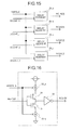
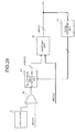
- Fig. 1 depicts the overall configuration of an oversampling circuit according to a first embodiment of the present invention.
- a reference clock REFCLK is put into a multiphase delay unit 1, and is put out as M bit multiphase clocks MCLK having phases different from each other.
- the reference clock REFCLK is acceptable when generated by an ordinary PLL circuit, etc., which is a known technique, and therefore will not be described in detail.
- External input serial data SDATA is sampled at a multiphase sampling unit 2, using each of the multiphase clocks MCLK, and is put out as M bit multiphase data MDATA.
- a phase selecting unit 3 selects a proper data out of the multiphase data MDATA, and puts out the selected data as N bit over sample data NDATA. In this process, M>N must be satisfied.
- Fig. 2 depicts an example of a timing chart of input/output signals at the multiphase delay unit 1 incorporated in the oversampling circuit shown in Fig. 1.
- MCLK[k] denotes kth bit of the multiphase clocks MCLK, and the same notational convention will be adopted appropriately in the following description.
- the M bit multiphase clocks MCLK are put out in delay at respective delay times ⁇ _0 to ⁇ _(M-1) relative to the input reference clock REFCLK, which delay times are different from each other.
- ⁇ _0 represents the delay time from a rising edge of the reference clock REFCLK to a rising edge of the multiphase clock MCLK[0], and the same notational convention will be used in the description to follow.
- the delay times ⁇ _0 to ⁇ _(M-1) are equal in terms of interval to some extent, but are not required to be strictly equal.
- ⁇ _(M-1)- ⁇ _0>T must be satisfied when the cycle of the reference clock REFCLK is T.
- Fig. 3 depicts one embodiment of the multiphase delay unit 1 incorporated in the oversampling circuit shown in Fig. 1.
- the input reference clock REFCLK is put in parallel into M units of inverters 4_a to 4_n, which send their output further to M units of inverters 5_a to 5_n, which then put out the M bit multiphase clocks MCLK.
- the inverters 5_a to 5_n are all identical in size, but the inverters 4_a to 4_n are different from each other in size (drive capability).
- the risetimes and falltimes of a signal driven by an inverter are determined by the size of inverter driving the signal and a load capacitance attached to the output node of the inverter.
- gradually changing the size of the inverters 4_a to 4_n to gradually shift the phases of clocks put out of the inverters to be able to generate the M bit multiphase clocks MCLK as shown in Fig. 2.
- Fig. 4 depicts one embodiment of the multiphase sampling unit 2 incorporated in the oversampling circuit shown in Fig. 1.
- the external input serial data SDATA is put into M units of flip-flops 6a to 6n, where the input data is sampled at rising edges of the M bit multiphase clocks MCLK generated by the multiphase delay unit 1, respectively.
- Sampled M bit data MODATA are then delayed for proper delay times at a delay unit 7, and are sampled again through M units of flip-flops 10_a to 10_n, respectively, at which a sampling clock SCLK common to every pieces of data is used.
- This sampling clock SCLK is generated by properly delaying the reference clock REFCLK or one of the multiphase clocks MCLK.
- the delay unit 7 has the internal configuration same as that shown in Fig. 3, being composed of inverters 8_a to 8_n and 9_a to 9_n.
- the size of the inverters 8_a to 8_n and 9_a to 9_n, therefore, is so selected as to ensure the constant total delay time ⁇ tot_k ⁇ _k+ ⁇ '_k.
- Fig. 5 depicts one embodiment of the phase selecting unit 3 incorporated in the oversampling circuit shown in Fig. 1.
- the incoming M bit multiphase data MDATA is put into a UI (Unit Interval: 1 bit data length) detecting unit 11, an edge counter 12, and a selecting unit 13.
- T denotes the cycle of the reference clock REFCLK.
- the edge counter 12 detects data transition (edge) present before kth bit of the M bit multiphase data MDATA, and counts an increment of a count value count_k upon detecting an edge.
- the edge counter 12 counts edges for every k satisfying 0 ⁇ k ⁇ M (or 0 ⁇ k ⁇ L).
- the selecting unit 13 selects a proper N bit data on the basis of a UI detection result and count values count_l 1 to count_(M-1), and puts out the selected data as the N bit over sample data NDATA.
- Fig. 6 depicts one embodiment of the UI detecting unit 11 incorporated in the phase selecting unit shown in Fig. 5.
- Output from the XOR gates 14_a to 14_m is put into (M-1) units of counters 15_a to 15_m, which count the number of times of "H" registered by the output from the XOR gates 14_a to 14_m, and put out resulting count values.
- a detector 16 detects the minimum count value out of the count values put out of respective counters 15_a to 15_m, and puts out the detected minimum count value.
- Fig. 7 depicts one embodiment of the edge counter 12 incorporated in the phase selecting unit shown in Fig. 5.
- Incoming M bit multiphase data MDATA is put into XOR gates 18_a to 18_m in such a way that each pair of data adjacent in phase is put into each of the XOR gates.
- Output from the XOR gates 18_a to 18_m is put into counters 19_a to 19_m, and output from the counters 19_a to 19_m is then put into adders 20_a to 20_l, which calculate the sum of each input from the counters.
- the total numbers of edges before respective bits of the M bit multiphase data MDATA are counted, and are put out as count values count_ 1 to count_(M-1).
- Fig. 8 depicts an example of times of rising edges of multiphase clocks MCLK[k] defined by respective values of k, which times are represented by arrows on the horizontal axis, with regard to a reference of a rising edge of the multiphase clock MCLK[0] at the selecting unit shown in Fig. 5.
- Usual multiphase clocks should preferably have equal inter-phase intervals, but the inter-phase intervals are not equal in actual application, as shown in Fig. 8, because of layout-based variations in load capacitances and power fluctuation, functional dispersion of devices, etc.
- the equation means that the count value count_k represents a time difference between the multiphase clock MCLK[k] and the multiphase clock MCLK[0]. At this time, the time of 1 UI is given by count_L when L detected by the UI detecting unit 11 is used.
- the count value count_k is a monotonic increasing function with respect to k, which enables detection of a proper L_a.
- a delay time at the multiphase delay unit 1 changes dynamically due to the fluctuation of power voltage and temperature.
- a clock at a desired phase can be selected constantly by carrying out the above phase detection constantly or at every a given time interval, or by monitoring the fluctuation of power voltage and temperature and carrying out phase detection when the fluctuation reaches a certain amount.
- counting operation must be carried out for a given time TO or longer.
- the time TO must satisfies at least the condition: TO > 1 / Ftx - Frx
- a receiver having a configuration shown in Fig. 10 is used preferably.
- This receiver is provided by adding an oscillator 21 and a selector 22 to the oversampling circuit of the embodiment shown in Fig. 1.
- the oscillator 21 is completely asynchronous with the reference clock REFCLK, and oscillates at a proper frequency F1.
- the selector 22 puts the serial data SDATA into the multiphase sampling unit 2, in which case the phase selecting unit 3 selects a given phase.
- the selector 22 When input data is not needed, such as a time of circuit startup or an idle state in input reception, the selector 22 sends output from the oscillator 21 into the multiphase sampling unit 2, in which case the phase selecting unit 3 carries out calibration operation of executing the above counting operation to determine a phase L_a to select.
- a delay time given by the multiphase delay unit 1 changes dynamically, as described above, so that the calibration operation is carried out properly according to a need. If the frequency F1 of the oscillator 21 is approximately the same as the frequency Frx of the reference clock REFCLK, the counting time TO must satisfy at least the condition: TO > 1 / F ⁇ 1 - Frx
- the counting time TO must satisfy the condition: TO > p / Fl - Frx
- a delay time given by the multiphase delay unit 1 changes due to a layout-based parasitic capacitance, local fluctuation of power voltage caused by switching current, etc., thus often does not follow a designer's intention, which may even cause phase reversal in the multiphase clocks MCLK.
- a receiver having a configuration shown Fig. 11 is used preferably.
- This receiver is provided by adding a digital filter 23 having proper low-pass characteristics to the oversampling circuit of the embodiment shown in Fig. 1.
- the digital filter 23 is provided by using a known FIR (Finite Impulse Response) filter or an IIR (Infinite Impulse Response) filter.
- FIR Finite Impulse Response
- IIR Infinite Impulse Response
- a part of a filter that is a tertiary FIR filter provided as the digital filter 23 is shown in Fig. 12, and a detailed operational example of such a filter is shown in Fig. 13.
- a filter order and circuit configuration may be selected properly according to a need.
- the input multiphase data MDATA is added up by an adder 24, and then is binarized using a proper threshold at a binarizing unit 25.
- the selecting unit can be used using the multiphase data MDATA put out of the filter.
- data is taken in using multiphase clocks generated on the basis of one reference clock, the edges of the data pattern are counted to estimate the phase relation of the multiphase clocks, and data taken in at a clock having a proper phase is put out as oversampling data.
- the dispersion of clock phases due to power/temperature fluctuation, functional dispersion of devices, etc. is corrected to be able to carry out precise oversampling of the input data.
- sampled data is used for phase detection, a detection error can be reduced.
- the reference clock used for the circuit is acceptable if it has a single phase, and the multiphase clocks are used for sampling immediately after being generated. This eliminates a need of transmitting the multiphase clocks, allowing a smaller circuit scale, thus leading to a reduction in chip size and power consumption.
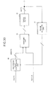
- Fig. 14 depicts the overall configuration of an oversampling circuit according to a second embodiment of the present invention.
- a multiphase delay control unit 26 delays the reference clock REFCLK, and puts it out as N bit multiphase clocks NCLK. In delaying the reference clock REFCLK, a delay time for each phase is controlled by a delay control signal DCONT.
- the external input serial data SDATA is sampled using respective multiphase clocks NCLK at a multiphase sampling unit 27, and is put out as the N bit over sample data NDATA.
- a phase detecting unit 28 detects the phases of the multiphase clocks NCLK on the basis of the over sample data NDATA, and puts out a proper delay control signal DCONT.
- Fig. 15 depicts the detailed configuration of the multiphase delay control unit 26 incorporated in the oversampling circuit shown in Fig. 14.
- the reference clock REFCLK is put into delay elements 29_a to 29_d, which delay the input reference clock REFCLK for different delay times ⁇ _0 to ⁇ _(N-1) to put out respective N bit multiphase clocks NCLK.
- the delay times ⁇ _0 to ⁇ _(N-1) are controlled by control signals DCONT_0 to DCONT_(N-1), respectively.
- DCONT_k means the delay control signal DCONT for the multiphase clock NCLK[k], and the same notational convention will be used in the following description.
- each of the delay elements 29_a to 29_d is shown in Fig. 16.
- the control signal DCONT controls current supply from current sources 30_a and 30_b to control the risetimes and falltimes of a signal driven by a PMOS transistor 31 and a PMOS transistor 32, thus separately controls respective delay times of the delay elements 29_a to 29_d.
- Fig. 17 depicts another embodiment of the multiphase sampling unit 27 incorporated in the oversampling circuit according to the present invention.
- the input serial data SDATA is sampled at flip-flops 34_a to 34_d using the N bit multiphase clocks NCLK, is delayed at delay elements 35_a to 35_d, is synchronized with the sampling clock SCLK at flip-flops 36_a to 36_d, and then is put out as the N bit multiphase data NDATA.
- the delay times ⁇ '_0 to ⁇ '_(N-1) of the delay elements 35_a to 35_d are controlled by the delay control signals DCONT_0 to DCONT_(N-1), respectively.
- the total delay time ⁇ tok_k that is, the sum of the delay time ⁇ _k, which is given by the multiphase delay control unit 26, and the delay time ⁇ '_k should desirably be constant with respect to the value of k.
- Fig. 18 depicts one embodiment of the phase detecting unit 28 incorporated in the oversampling circuit shown in Fig. 14.
- An edge counter 37 counts edges for each bit of the input N bit over sample data NDATA, and puts out a count result as a count value ncount.
- a calculating unit 38 puts out the delay control signal DCOUNT on the basis of the count value ncount.
- Fig. 19 depicts one embodiment of the edge counter 37 incorporated in the phase detecting unit shown in Fig. 18.
- edges of the N bit multiphase data NDATA are detected for adjacent bits at XOR gates 39_a to 39_d, and the detected edges are counted at counters 40_a to 40_c.
- the data NDATA[0] is delayed by one cycle and is compared with the data NDATA[N-1], and the resulted number of edges is counted at the counter 40_d.
- Output from each of the counters 40_a to 40_d is put into each of adders 41_a to 41_c, which calculates the sum of each output from the counters.
- Fig. 20 depicts one embodiment of the calculating unit 38 incorporated in the phase detecting unit shown in Fig. 18.
- the comparators 44_a to 44_c compare the calculation results from the multipliers/dividers 43_a to 43_c with the count value ncount_k, respectively, and put out the delay control signal DCOUNT for each of the N bit multiphase clocks NCLK on the basis of the result of comparison.
- the count value ncount_k represents a time difference between the N bit clock NCLK_k and the N bit clock NCLK_0 when the edges of the input signal SDATA is distributed uniformly relative to the referenced clock REFCLK. For this reason, when the delay control signal DCONT is given a proper value so that each value taken by ncount_k is equivalent to 1/N of the count value ncount_N, the N bit multiphase clocks NCLK have phases each equivalent to 1/N of T.
- a delay time at the multiphase delay unit 1 changes dynamically due to the fluctuation of power voltage and temperature. For this reason, the above control through phase detection is carried out constantly or at every a given time interval, or carried out properly when the monitored fluctuation of power voltage and temperature reaches a certain amount. In this way, a clock at a desired phase can be selected constantly.
- This receiver is provided by connecting the oscillator 21 and the selector 22 to the oversampling circuit of the embodiment shown in Fig. 14.
- the detailed operation of the oscillator 21 and selector 22 is virtually the same as that of the embodiment shown in Fig. 10, and is therefore not described further in detail. If the frequency F1 of the oscillator 21 is approximately the same as the frequency Frx of the reference clock REFCLK, the counting time TO must satisfy at least the condition: TO>1/
- a receiver having a configuration shown Fig. 22 is used preferably.
- This receiver is provided by adding a digital filter 45 having proper low-pass characteristics to the oversampling circuit of the embodiment shown in Fig. 14.
- the operation of the digital filter 45 is the same as that of the digital filter of the first embodiment, and is therefore not described further in detail.
- data is taken in using multiphase clocks generated on the basis of one reference clock, the edges of the data pattern are counted to estimate the phase relation of the multiphase clocks, and control is performed to make the phases of the multiphase clocks proper one.
- the dispersion of clock phases due to power/temperature fluctuation, functional dispersion of devices, etc. is corrected to be able to carry out precise oversampling of the input data. Since sampled data is used for phase detection, a detection error can be reduced.
- the reference clock used for the circuit is acceptable if it has a single phase, and the multiphase clocks are used for sampling immediately after being generated. This eliminates a need of transmitting the multiphase clocks, allowing a smaller circuit scale, thus leading to a reduction in chip size and power consumption.
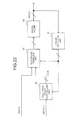
- Fig. 23 depicts the overall configuration of an oversampling circuit according to a third embodiment of the present invention.
- the serial data SDATA is put into a multiphase delay unit 46, and is put out as M bit multiphase delay data dMDATA having phases different from each other.
- the M bit multiphase delay data dMDATA is sampled using the reference clock REFCLK at a sampling unit 47, and is put out as the M bit multiphase data MDATA.
- the reference clock REFCLK is acceptable when generated by an ordinary PLL circuit, etc., which is a known technique, and is therefore not described in detail.
- the phase selecting unit 3 selects a proper data out of the multiphase data MDATA, and puts out the selected data as the N bit over sample data NDATA. In this process, M>N must be satisfied.
- the multiphase delay unit 46 is provided by using the multiphase delay unit having the same configuration as shown in Fig. 3. However, the multiphase delay unit 46 receives input of the serial data SDATA, and puts out the M bit multiphase delay data dMDATA.
- the multiphase delay unit 46 is different from the multiphase delay unit of the first embodiment in the point that a delay time given for the delay data dMDATA[0] is the maximum and a delay time given for the delay data dMDATA[M-1] is the minimum.
- M units of flip-flops 48_a to 48__n take in all M bit multiphase delay data dMDATA using the reference clock REFCLK.
- This embodiment is different from the first embodiment in the point that the data itself is delayed already, so that a single clock can be used as a clock for sampling the data. The data taken in, therefore, can be put out directly as synchronized data.
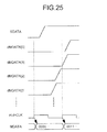
- Fig. 25 depicts an example of a timing chart of the multiphase delay unit 46 and the sampling unit 47 that are incorporated in the oversampling circuit shown in Fig. 23.
- the external input serial data SDATA is delayed at the multiphase delay unit 46, and is put out of the multiphase delay unit 46 as the M bit multiphase delay data dMDATA, which is then sampled at the sampling unit 47.
- the M bit multiphase data MDATA obtained through this process is the result of oversampling of the serial data SDATA.
- the constituent elements used in the following process therefore, can be provided as the same constituent elements as that of the first embodiment.
- phase selecting unit 3 is the same as that of the first embodiment, and is therefore not described further in detail. Since a delay time at the multiphase delay unit 46 changes dynamically, as described above, selection operation at the phase selecting unit 3 is carried out constantly or on a necessary basis. This condition is also the same as one mentioned before, and is therefore not described further in detail.
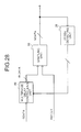
- Fig. 26 depicts a receiver constructed by adding the oscillator 21 and the selector 22 to the oversampling circuit shown in Fig. 23 for calibration operation. This receiver is not described further in detail. Phase reversal may happen in the multiphase delay unit 46, and a receiver having an additional component of the digital filter 23 as shown in Fig. 27 may be used to deal with the phase reversal problem.
- This receiver has the same configuration as the configurative example shown in Fig. 11, and is therefore not described further in detail.
- multiphase delay data generated by delaying input serial data is taken in using a single clock, the edges of the data pattern are counted to estimate the phase relation of the multiphase delay data, and data that is properly delayed and sampled is put out as oversampling data.
- the dispersion of clock phases due to power/temperature fluctuation, functional dispersion of devices, etc. is corrected to be able to carry out precise oversampling of the input data. Since sampled data is used for phase detection, a detection error can be reduced.
- the data is delayed and turned into multiphase data, so that a single clock suffices for sampling and phase alignment following sampling is not necessary. This allows a smaller circuit scale, leading to a reduction in chip size and power consumption.
- Fig. 28 depicts the overall configuration of an oversampling circuit according to a fourth embodiment of the present invention.
- a multiphase delay control unit 49 delays the input serial data SDATA, and put it out as N bit multiphase delay data dNDATA. In delaying the serial data SDATA, a delay time for each phase is controlled by each of delay control signals DCONT_0 to DCONT_(N-1).
- the N bit multiphase delay data dNDATA is sampled using the reference clock REFCLK at a sampling unit 50, and is put out as the N bit over sample data NDATA.
- the phase detecting unit 28 detects the phases of the multiphase clocks NCLK on the basis of the over sample data NDATA, and puts out proper delay control signals DCONT_0 to DCONT_(N-1).
- the multiphase delay control unit 49 is provided as the multiphase delay control unit having the configuration shown in Fig. 15. The multiphase delay control unit 49, however, receives input of the serial data SDATA and puts out the N bit multiphase delay data dNDATA.
- the multiphase delay control unit 49 is different from the multiphase delay control unit of the second embodiment in the point that a delay time given for the delay data dNDATA[0] is the maximum and a delay time given for the delay data dNDATA[N-1] is the minimum.
- the sampling unit is so configured as to put the incoming multiphase delay data dNDATA into flip-flops to sample the data using the reference clock REFCLK. This configuration is virtually the same as the configuration shown in Fig. 24, and is therefore not described further in detail.
- the phase detecting unit 28 is the same as that of the second embodiment, and is therefore not described further in detail. Since a delay time at the multiphase delay unit 46 changes dynamically, as described above, selection operation at the phase detecting unit 28 is carried out constantly or on a necessary basis. This condition is also the same as one mentioned before, and is therefore not described further in detail.
- Fig. 29 depicts a receiver provided with additional components of the oscillator 21 and the selector 22 for calibration operation. This receiver is not described further in detail. Phase reversal may happen in the multiphase delay control unit 49, and a receiver having an additional component of the digital filter 45 as shown in Fig. 30 may be used to deal with the phase reversal problem. This receiver has the same configuration as the configurative example shown in Fig. 11, and is therefore not described further in detail.
- multiphase delay data generated by delaying input serial data is taken in using a single clock, the edges of the data pattern are counted to estimate the phase relation of the multiphase delay data, and control is performed to make the phases of the multiphase delay data proper one.
- the dispersion of clock phases due to power/temperature fluctuation, functional dispersion of devices, etc. is corrected to be able to carry out precise oversampling of the input data. Since sampled data is used for phase detection, a detection error can be reduced.
- the data is delayed and turned into multiphase data, so that a single clock suffices for sampling and phase alignment following sampling is not necessary. This allows a smaller circuit scale, leading to reduction in chip size and power consumption.
- multiphase clocks are generated on the basis of a reference clock to sample external input serial data using the multiphase clocks, the phase relation of the multiphase clocks is detected from the edges of a data pattern obtained by the sampling, and data having a proper phase is selected and put out as oversampling data.
- This process allows the dispersion of delay times for the multiphase clocks to be generated, which enables substantial reduction in trouble with circuit layout and power supply design.
- the process also allows a delay circuit of a simple structure, which leads to reduction in circuit scale, chip size, and power consumption.
- phase detection is carried out using sampled digital data, which enables highly precise phase detection.
- multiphase clocks are generated on the basis of a reference clock to sample external input serial data using the multiphase clocks, the phase relation of the multiphase clocks is detected from the edges of a data pattern obtained by the sampling, and delay times given upon generating the multiphase clocks are controlled for respective phases.
- This process allows the functional dispersion of delay circuits generating the multiphase clocks, which enables substantial reduction in trouble with circuit layout and power supply arrangement.
- the process also allows the delay circuit of a simple structure, which leads to a reduction in circuit scale, chip size, and power consumption.
- phase detection is carried out using sampled digital data, which enables highly precise phase detection. The number of clocks for phase detection can be reduced to the minimum necessary number, which enables further reduction in circuit scale.
- multiphase data is generated on the basis of external input serial data to sample the multiphase data using a reference clock, the phase relation of the multiphase data is detected from the edges of a data pattern obtained by the sampling, and data having a proper phase is selected and put out as oversampling data.
- This process allows the dispersion of delay times for the multiphase data to be generated, which enables a substantial reduction in trouble with circuit layout and power supply design.
- the process also allows a delay circuit of a simple structure, which leads to a reduction in circuit scale, chip size, and power consumption.
- phase detection is carried out using sampled digital data, which enables highly precise phase detection.
- the clock used for sampling has a single phase, thus can be used directly on a digital circuit, which allows further reduction in circuit scale.
- multiphase data is generated on the basis of external input serial data to sample the multiphase data using a reference clock, the phase relation of the multiphase data is detected from the edges of a data pattern obtained by the sampling, and delay times given upon generating the multiphase data are controlled for respective phases.
- This process allows the dispersion of delay times for the multiphase clocks to be generated, which enables a substantial reduction in trouble with circuit layout and power supply arrangement.
- the process also allows a delay circuit of a simple structure, which leads to reduction in circuit scale, chip size, and power consumption.
- phase detection is carried out using sampled digital data, which enables highly precise phase detection.
- the number of clocks for phase detection can be reduced to the minimum necessary number, which enables further reduction in circuit scale.
- the clock used for sampling has a single phase, thus can be used directly on a digital circuit, which enables further reduction in circuit scale.
- provided the circuit with a proper oscillation circuit enables accurate phase detection even if the transmission side is completely synchronized with the reference clock.
- providing the circuit with a digital filter allows detection of a clock having a correct phase even if phase reversal is happening in the multiphase clocks.
- the oscillator and digital filter are each provided by using a simple circuit and yet offer a sufficient effect.
- delay times for the multiphase clocks to generate are allowed to be different from each other, which remarkably reduces trouble with circuit layout and power supply design.
- a delay circuit is allowed to be simply configured, which leads to a reduction in circuit scale, chip size, and power consumption.
- Phase detection is carried out using sampled digital data, which enables highly precise phase detection. Thus, data subjected to oversampling at phases having equal intervals can be generated.
- every circuit is considered to be equivalent when multiphase clocks are generated, but the multiphase clocks are generated using a delay unit having respective different delay times, and data subjected to oversampling at phases having equal intervals is generated on the basis of sampling data obtained by using the multiphase clocks.
- phase detection is carried out using sampled digital data, so that highly precise phase detection can be carried out with a small-scale circuit.
- the data subjected to oversampling at phases having equal intervals therefore, can be generated.
Landscapes
- Engineering & Computer Science (AREA)
- Computer Networks & Wireless Communication (AREA)
- Signal Processing (AREA)
- Synchronisation In Digital Transmission Systems (AREA)
- Dc Digital Transmission (AREA)
Applications Claiming Priority (1)
| Application Number | Priority Date | Filing Date | Title |
|---|---|---|---|
| JP2006240668A JP2008066879A (ja) | 2006-09-05 | 2006-09-05 | オーバーサンプリング回路及びオーバーサンプリング方法 |
Publications (1)
| Publication Number | Publication Date |
|---|---|
| EP1898548A1 true EP1898548A1 (en) | 2008-03-12 |
Family
ID=38657110
Family Applications (1)
| Application Number | Title | Priority Date | Filing Date |
|---|---|---|---|
| EP07115066A Withdrawn EP1898548A1 (en) | 2006-09-05 | 2007-08-28 | Oversampling circuit and oversampling method |
Country Status (3)
| Country | Link |
|---|---|
| US (1) | US8023605B2 (ja) |
| EP (1) | EP1898548A1 (ja) |
| JP (1) | JP2008066879A (ja) |
Cited By (1)
| Publication number | Priority date | Publication date | Assignee | Title |
|---|---|---|---|---|
| US9191020B2 (en) | 2014-02-05 | 2015-11-17 | Waveworks, Inc. | Traveling-wave based high-speed sampling systems |
Families Citing this family (10)
| Publication number | Priority date | Publication date | Assignee | Title |
|---|---|---|---|---|
| JP2009049600A (ja) * | 2007-08-16 | 2009-03-05 | Ricoh Co Ltd | 差動信号出力装置 |
| JP5423071B2 (ja) * | 2009-03-13 | 2014-02-19 | 株式会社ニコン | データ転送装置及び撮像装置 |
| WO2011004580A1 (ja) * | 2009-07-06 | 2011-01-13 | パナソニック株式会社 | クロックデータリカバリ回路 |
| US8416902B2 (en) * | 2010-01-14 | 2013-04-09 | Ian Kyles | Clock and data recovery for burst-mode serial signals |
| JP2012109931A (ja) | 2010-10-25 | 2012-06-07 | Ricoh Co Ltd | オーバーサンプリング回路及びそれを用いたシリアル通信装置及びシリアル通信方法 |
| US20150207617A1 (en) * | 2014-01-22 | 2015-07-23 | Kabushiki Kaisha Toshiba | Reception circuit and communication system |
| TWI554037B (zh) * | 2015-04-16 | 2016-10-11 | 群聯電子股份有限公司 | 時脈資料回復電路模組、記憶體儲存裝置及相位鎖定方法 |
| JP2017135506A (ja) | 2016-01-26 | 2017-08-03 | 株式会社日立製作所 | スキュー調整回路、半導体装置およびスキューキャリブレーション方法 |
| US20230344432A1 (en) * | 2022-04-26 | 2023-10-26 | International Business Machines Corporation | Asymmetrical clock separation and stage delay optimization in single flux quantum logic |
| CN118074711B (zh) * | 2024-04-19 | 2024-08-02 | 南京仁芯科技有限公司 | 一种车载SerDes芯片、包括其的汽车配件及汽车 |
Citations (7)
| Publication number | Priority date | Publication date | Assignee | Title |
|---|---|---|---|---|
| US5003562A (en) * | 1989-10-27 | 1991-03-26 | Ncr Corporation | Digital phase lock loop decoder |
| US6122335A (en) * | 1999-10-01 | 2000-09-19 | Quantum Bridge Communications, Inc. | Method and apparatus for fast burst mode data recovery |
| EP1363399A2 (en) * | 2002-05-17 | 2003-11-19 | NEC Electronics Corporation | Clock and data recovery circuit and clock control method thereof |
| US20040239546A1 (en) * | 2003-05-29 | 2004-12-02 | Takamoto Watanabe | A/d conversion method and apparatus |
| US20040258410A1 (en) * | 2003-06-17 | 2004-12-23 | Yusuke Yajima | Bit synchronization circuit and central terminal for PON systems |
| EP1538775A1 (en) * | 2003-12-05 | 2005-06-08 | Ricoh Company, Ltd. | Data recovery method and data recovery circuit |
| US20060109942A1 (en) * | 2003-12-19 | 2006-05-25 | International Business Machines Corporation | Improvements to data recovery circuits using oversampling for best data sample selection |
Family Cites Families (6)
| Publication number | Priority date | Publication date | Assignee | Title |
|---|---|---|---|---|
| JPH0614638B2 (ja) * | 1985-07-31 | 1994-02-23 | セルヴル ミシエル | 局部クロック信号と受信データ信号とを再同期させる機構 |
| JPH0479632A (ja) * | 1990-07-23 | 1992-03-13 | Nec Corp | ビット位相同期回路 |
| JP2000031951A (ja) * | 1998-07-15 | 2000-01-28 | Fujitsu Ltd | バースト同期回路 |
| JP3414700B2 (ja) | 1999-06-15 | 2003-06-09 | シャープ株式会社 | 多相クロックの位相ずれ量検出回路およびそれを用いたビット同期回路 |
| JP3636657B2 (ja) | 2000-12-21 | 2005-04-06 | Necエレクトロニクス株式会社 | クロックアンドデータリカバリ回路とそのクロック制御方法 |
| KR100615597B1 (ko) * | 2004-05-27 | 2006-08-25 | 삼성전자주식회사 | 데이터 입력회로 및 방법 |
-
2006
- 2006-09-05 JP JP2006240668A patent/JP2008066879A/ja active Pending
-
2007
- 2007-08-27 US US11/845,416 patent/US8023605B2/en not_active Expired - Fee Related
- 2007-08-28 EP EP07115066A patent/EP1898548A1/en not_active Withdrawn
Patent Citations (7)
| Publication number | Priority date | Publication date | Assignee | Title |
|---|---|---|---|---|
| US5003562A (en) * | 1989-10-27 | 1991-03-26 | Ncr Corporation | Digital phase lock loop decoder |
| US6122335A (en) * | 1999-10-01 | 2000-09-19 | Quantum Bridge Communications, Inc. | Method and apparatus for fast burst mode data recovery |
| EP1363399A2 (en) * | 2002-05-17 | 2003-11-19 | NEC Electronics Corporation | Clock and data recovery circuit and clock control method thereof |
| US20040239546A1 (en) * | 2003-05-29 | 2004-12-02 | Takamoto Watanabe | A/d conversion method and apparatus |
| US20040258410A1 (en) * | 2003-06-17 | 2004-12-23 | Yusuke Yajima | Bit synchronization circuit and central terminal for PON systems |
| EP1538775A1 (en) * | 2003-12-05 | 2005-06-08 | Ricoh Company, Ltd. | Data recovery method and data recovery circuit |
| US20060109942A1 (en) * | 2003-12-19 | 2006-05-25 | International Business Machines Corporation | Improvements to data recovery circuits using oversampling for best data sample selection |
Cited By (1)
| Publication number | Priority date | Publication date | Assignee | Title |
|---|---|---|---|---|
| US9191020B2 (en) | 2014-02-05 | 2015-11-17 | Waveworks, Inc. | Traveling-wave based high-speed sampling systems |
Also Published As
| Publication number | Publication date |
|---|---|
| JP2008066879A (ja) | 2008-03-21 |
| US8023605B2 (en) | 2011-09-20 |
| US20080056420A1 (en) | 2008-03-06 |
Similar Documents
| Publication | Publication Date | Title |
|---|---|---|
| US8023605B2 (en) | Oversampling circuit and oversampling method | |
| CN113841334B (zh) | 多相时钟占空比与时偏的测量和校正 | |
| US7474720B2 (en) | Clock and data recovery method and digital circuit for the same | |
| US8559582B2 (en) | Techniques for varying a periodic signal based on changes in a data rate | |
| KR100574938B1 (ko) | 고속 직렬 링크에서 데이터 복원시 에러 발생을감소시키는 데이터 복원장치 및 그 복원방법 | |
| US7756232B2 (en) | Clock and data recovery circuit | |
| JP3990570B2 (ja) | プログラマブルロジックデバイス回路に結合されるクロックデータリカバリ回路 | |
| US20170214515A1 (en) | Phase Control Block for Managing Multiple Clock Domains in Systems with Frequency Offsets | |
| US7599457B2 (en) | Clock-and-data-recovery system having a multi-phase clock generator for one or more channel circuits | |
| KR0153952B1 (ko) | 고속 디지털 데이터 리타이밍 장치 | |
| US7482841B1 (en) | Differential bang-bang phase detector (BBPD) with latency reduction | |
| US8537947B2 (en) | Oversampling circuit, serial communication apparatus and oversampling method | |
| US5689530A (en) | Data recovery circuit with large retime margin | |
| US6970521B2 (en) | Circuit and system for extracting data | |
| JP2010147558A (ja) | クロックデータリカバリ回路 | |
| US20040114702A1 (en) | Bang-bang phase detector for full-rate and half-rate schemes clock and data recovery and method therefor | |
| JP2014222872A (ja) | クロック・データ・リカバリ回路で受信データ信号をトラッキングするためのシステム及び方法 | |
| JP5520128B2 (ja) | クロックアンドデータリカバリ回路 | |
| US5592519A (en) | Dual frequency clock recovery using common multitap line | |
| JP2014225874A (ja) | クロック・データ・リカバリ回路で受信データ信号を取得するためのシステム及び方法 | |
| KR20080051662A (ko) | 데이터 속도의 1/4 주파수 클럭을 사용하는 고속의 클럭 및데이터 복원 회로 및 방법 | |
| US7321647B2 (en) | Clock extracting circuit and clock extracting method | |
| Tejera et al. | High-speed clock recovery unit based on a phase aligner |
Legal Events
| Date | Code | Title | Description |
|---|---|---|---|
| PUAI | Public reference made under article 153(3) epc to a published international application that has entered the european phase |
Free format text: ORIGINAL CODE: 0009012 |
|
| AK | Designated contracting states |
Kind code of ref document: A1 Designated state(s): AT BE BG CH CY CZ DE DK EE ES FI FR GB GR HU IE IS IT LI LT LU LV MC MT NL PL PT RO SE SI SK TR |
|
| AX | Request for extension of the european patent |
Extension state: AL BA HR MK YU |
|
| 17P | Request for examination filed |
Effective date: 20080603 |
|
| AKX | Designation fees paid |
Designated state(s): DE ES FR GB IT NL |
|
| 17Q | First examination report despatched |
Effective date: 20161221 |
|
| STAA | Information on the status of an ep patent application or granted ep patent |
Free format text: STATUS: THE APPLICATION HAS BEEN WITHDRAWN |
|
| 18W | Application withdrawn |
Effective date: 20170206 |