EP1863003A2 - Einheitsschaltung, elektrooptische Vorrichtung und elektronisches Gerät - Google Patents
Einheitsschaltung, elektrooptische Vorrichtung und elektronisches Gerät Download PDFInfo
- Publication number
- EP1863003A2 EP1863003A2 EP07010494A EP07010494A EP1863003A2 EP 1863003 A2 EP1863003 A2 EP 1863003A2 EP 07010494 A EP07010494 A EP 07010494A EP 07010494 A EP07010494 A EP 07010494A EP 1863003 A2 EP1863003 A2 EP 1863003A2
- Authority
- EP
- European Patent Office
- Prior art keywords
- electrode
- node
- capacitive element
- potential
- period
- Prior art date
- Legal status (The legal status is an assumption and is not a legal conclusion. Google has not performed a legal analysis and makes no representation as to the accuracy of the status listed.)
- Withdrawn
Links
- 230000014509 gene expression Effects 0.000 description 26
- 230000008859 change Effects 0.000 description 20
- 238000010586 diagram Methods 0.000 description 13
- 230000004048 modification Effects 0.000 description 13
- 238000012986 modification Methods 0.000 description 13
- 239000003990 capacitor Substances 0.000 description 10
- 230000000694 effects Effects 0.000 description 7
- 230000003071 parasitic effect Effects 0.000 description 7
- 230000008878 coupling Effects 0.000 description 5
- 238000010168 coupling process Methods 0.000 description 5
- 238000005859 coupling reaction Methods 0.000 description 5
- 238000007689 inspection Methods 0.000 description 5
- 230000001413 cellular effect Effects 0.000 description 3
- 239000004973 liquid crystal related substance Substances 0.000 description 3
- 230000008901 benefit Effects 0.000 description 2
- 230000003287 optical effect Effects 0.000 description 2
- 230000004044 response Effects 0.000 description 2
- 238000000018 DNA microarray Methods 0.000 description 1
- 230000000052 comparative effect Effects 0.000 description 1
- 239000000463 material Substances 0.000 description 1
- 239000011159 matrix material Substances 0.000 description 1
- 230000005855 radiation Effects 0.000 description 1
- 239000000758 substrate Substances 0.000 description 1
- 230000007704 transition Effects 0.000 description 1
- 238000002834 transmittance Methods 0.000 description 1
Images






Classifications
-
- G—PHYSICS
- G09—EDUCATION; CRYPTOGRAPHY; DISPLAY; ADVERTISING; SEALS
- G09G—ARRANGEMENTS OR CIRCUITS FOR CONTROL OF INDICATING DEVICES USING STATIC MEANS TO PRESENT VARIABLE INFORMATION
- G09G3/00—Control arrangements or circuits, of interest only in connection with visual indicators other than cathode-ray tubes
- G09G3/20—Control arrangements or circuits, of interest only in connection with visual indicators other than cathode-ray tubes for presentation of an assembly of a number of characters, e.g. a page, by composing the assembly by combination of individual elements arranged in a matrix no fixed position being assigned to or needed to be assigned to the individual characters or partial characters
- G09G3/22—Control arrangements or circuits, of interest only in connection with visual indicators other than cathode-ray tubes for presentation of an assembly of a number of characters, e.g. a page, by composing the assembly by combination of individual elements arranged in a matrix no fixed position being assigned to or needed to be assigned to the individual characters or partial characters using controlled light sources
- G09G3/30—Control arrangements or circuits, of interest only in connection with visual indicators other than cathode-ray tubes for presentation of an assembly of a number of characters, e.g. a page, by composing the assembly by combination of individual elements arranged in a matrix no fixed position being assigned to or needed to be assigned to the individual characters or partial characters using controlled light sources using electroluminescent panels
-
- G—PHYSICS
- G09—EDUCATION; CRYPTOGRAPHY; DISPLAY; ADVERTISING; SEALS
- G09G—ARRANGEMENTS OR CIRCUITS FOR CONTROL OF INDICATING DEVICES USING STATIC MEANS TO PRESENT VARIABLE INFORMATION
- G09G3/00—Control arrangements or circuits, of interest only in connection with visual indicators other than cathode-ray tubes
- G09G3/20—Control arrangements or circuits, of interest only in connection with visual indicators other than cathode-ray tubes for presentation of an assembly of a number of characters, e.g. a page, by composing the assembly by combination of individual elements arranged in a matrix no fixed position being assigned to or needed to be assigned to the individual characters or partial characters
- G09G3/22—Control arrangements or circuits, of interest only in connection with visual indicators other than cathode-ray tubes for presentation of an assembly of a number of characters, e.g. a page, by composing the assembly by combination of individual elements arranged in a matrix no fixed position being assigned to or needed to be assigned to the individual characters or partial characters using controlled light sources
- G09G3/30—Control arrangements or circuits, of interest only in connection with visual indicators other than cathode-ray tubes for presentation of an assembly of a number of characters, e.g. a page, by composing the assembly by combination of individual elements arranged in a matrix no fixed position being assigned to or needed to be assigned to the individual characters or partial characters using controlled light sources using electroluminescent panels
- G09G3/32—Control arrangements or circuits, of interest only in connection with visual indicators other than cathode-ray tubes for presentation of an assembly of a number of characters, e.g. a page, by composing the assembly by combination of individual elements arranged in a matrix no fixed position being assigned to or needed to be assigned to the individual characters or partial characters using controlled light sources using electroluminescent panels semiconductive, e.g. using light-emitting diodes [LED]
- G09G3/3208—Control arrangements or circuits, of interest only in connection with visual indicators other than cathode-ray tubes for presentation of an assembly of a number of characters, e.g. a page, by composing the assembly by combination of individual elements arranged in a matrix no fixed position being assigned to or needed to be assigned to the individual characters or partial characters using controlled light sources using electroluminescent panels semiconductive, e.g. using light-emitting diodes [LED] organic, e.g. using organic light-emitting diodes [OLED]
- G09G3/3225—Control arrangements or circuits, of interest only in connection with visual indicators other than cathode-ray tubes for presentation of an assembly of a number of characters, e.g. a page, by composing the assembly by combination of individual elements arranged in a matrix no fixed position being assigned to or needed to be assigned to the individual characters or partial characters using controlled light sources using electroluminescent panels semiconductive, e.g. using light-emitting diodes [LED] organic, e.g. using organic light-emitting diodes [OLED] using an active matrix
- G09G3/3233—Control arrangements or circuits, of interest only in connection with visual indicators other than cathode-ray tubes for presentation of an assembly of a number of characters, e.g. a page, by composing the assembly by combination of individual elements arranged in a matrix no fixed position being assigned to or needed to be assigned to the individual characters or partial characters using controlled light sources using electroluminescent panels semiconductive, e.g. using light-emitting diodes [LED] organic, e.g. using organic light-emitting diodes [OLED] using an active matrix with pixel circuitry controlling the current through the light-emitting element
-
- G—PHYSICS
- G09—EDUCATION; CRYPTOGRAPHY; DISPLAY; ADVERTISING; SEALS
- G09G—ARRANGEMENTS OR CIRCUITS FOR CONTROL OF INDICATING DEVICES USING STATIC MEANS TO PRESENT VARIABLE INFORMATION
- G09G3/00—Control arrangements or circuits, of interest only in connection with visual indicators other than cathode-ray tubes
- G09G3/20—Control arrangements or circuits, of interest only in connection with visual indicators other than cathode-ray tubes for presentation of an assembly of a number of characters, e.g. a page, by composing the assembly by combination of individual elements arranged in a matrix no fixed position being assigned to or needed to be assigned to the individual characters or partial characters
- G09G3/22—Control arrangements or circuits, of interest only in connection with visual indicators other than cathode-ray tubes for presentation of an assembly of a number of characters, e.g. a page, by composing the assembly by combination of individual elements arranged in a matrix no fixed position being assigned to or needed to be assigned to the individual characters or partial characters using controlled light sources
- G09G3/30—Control arrangements or circuits, of interest only in connection with visual indicators other than cathode-ray tubes for presentation of an assembly of a number of characters, e.g. a page, by composing the assembly by combination of individual elements arranged in a matrix no fixed position being assigned to or needed to be assigned to the individual characters or partial characters using controlled light sources using electroluminescent panels
- G09G3/32—Control arrangements or circuits, of interest only in connection with visual indicators other than cathode-ray tubes for presentation of an assembly of a number of characters, e.g. a page, by composing the assembly by combination of individual elements arranged in a matrix no fixed position being assigned to or needed to be assigned to the individual characters or partial characters using controlled light sources using electroluminescent panels semiconductive, e.g. using light-emitting diodes [LED]
-
- G—PHYSICS
- G09—EDUCATION; CRYPTOGRAPHY; DISPLAY; ADVERTISING; SEALS
- G09G—ARRANGEMENTS OR CIRCUITS FOR CONTROL OF INDICATING DEVICES USING STATIC MEANS TO PRESENT VARIABLE INFORMATION
- G09G2300/00—Aspects of the constitution of display devices
- G09G2300/08—Active matrix structure, i.e. with use of active elements, inclusive of non-linear two terminal elements, in the pixels together with light emitting or modulating elements
- G09G2300/0809—Several active elements per pixel in active matrix panels
- G09G2300/0819—Several active elements per pixel in active matrix panels used for counteracting undesired variations, e.g. feedback or autozeroing
-
- G—PHYSICS
- G09—EDUCATION; CRYPTOGRAPHY; DISPLAY; ADVERTISING; SEALS
- G09G—ARRANGEMENTS OR CIRCUITS FOR CONTROL OF INDICATING DEVICES USING STATIC MEANS TO PRESENT VARIABLE INFORMATION
- G09G2300/00—Aspects of the constitution of display devices
- G09G2300/08—Active matrix structure, i.e. with use of active elements, inclusive of non-linear two terminal elements, in the pixels together with light emitting or modulating elements
- G09G2300/0809—Several active elements per pixel in active matrix panels
- G09G2300/0842—Several active elements per pixel in active matrix panels forming a memory circuit, e.g. a dynamic memory with one capacitor
- G09G2300/0852—Several active elements per pixel in active matrix panels forming a memory circuit, e.g. a dynamic memory with one capacitor being a dynamic memory with more than one capacitor
-
- G—PHYSICS
- G09—EDUCATION; CRYPTOGRAPHY; DISPLAY; ADVERTISING; SEALS
- G09G—ARRANGEMENTS OR CIRCUITS FOR CONTROL OF INDICATING DEVICES USING STATIC MEANS TO PRESENT VARIABLE INFORMATION
- G09G2300/00—Aspects of the constitution of display devices
- G09G2300/08—Active matrix structure, i.e. with use of active elements, inclusive of non-linear two terminal elements, in the pixels together with light emitting or modulating elements
- G09G2300/0809—Several active elements per pixel in active matrix panels
- G09G2300/0842—Several active elements per pixel in active matrix panels forming a memory circuit, e.g. a dynamic memory with one capacitor
- G09G2300/0861—Several active elements per pixel in active matrix panels forming a memory circuit, e.g. a dynamic memory with one capacitor with additional control of the display period without amending the charge stored in a pixel memory, e.g. by means of additional select electrodes
-
- G—PHYSICS
- G09—EDUCATION; CRYPTOGRAPHY; DISPLAY; ADVERTISING; SEALS
- G09G—ARRANGEMENTS OR CIRCUITS FOR CONTROL OF INDICATING DEVICES USING STATIC MEANS TO PRESENT VARIABLE INFORMATION
- G09G2320/00—Control of display operating conditions
- G09G2320/02—Improving the quality of display appearance
- G09G2320/0209—Crosstalk reduction, i.e. to reduce direct or indirect influences of signals directed to a certain pixel of the displayed image on other pixels of said image, inclusive of influences affecting pixels in different frames or fields or sub-images which constitute a same image, e.g. left and right images of a stereoscopic display
-
- G—PHYSICS
- G09—EDUCATION; CRYPTOGRAPHY; DISPLAY; ADVERTISING; SEALS
- G09G—ARRANGEMENTS OR CIRCUITS FOR CONTROL OF INDICATING DEVICES USING STATIC MEANS TO PRESENT VARIABLE INFORMATION
- G09G2320/00—Control of display operating conditions
- G09G2320/02—Improving the quality of display appearance
- G09G2320/0233—Improving the luminance or brightness uniformity across the screen
-
- G—PHYSICS
- G09—EDUCATION; CRYPTOGRAPHY; DISPLAY; ADVERTISING; SEALS
- G09G—ARRANGEMENTS OR CIRCUITS FOR CONTROL OF INDICATING DEVICES USING STATIC MEANS TO PRESENT VARIABLE INFORMATION
- G09G2320/00—Control of display operating conditions
- G09G2320/04—Maintaining the quality of display appearance
- G09G2320/043—Preventing or counteracting the effects of ageing
Definitions
- the present invention relates to a unit circuit that includes an electro-optical element, such as an organic light emitting diode (hereinafter referred to sometimes as OLED), an electro-optical device, and an electronic apparatus.
- an electro-optical element such as an organic light emitting diode (hereinafter referred to sometimes as OLED), an electro-optical device, and an electronic apparatus.
- OLED organic light emitting diode
- Display devices that use an organic light emitting diode are becoming popular.
- One such display device includes a plurality of pixels.
- Each of the pixels has an organic light emitting diode and a transistor that drives the OLED.
- To obtain a stable uniform display state in a plane it is necessary to cause the organic light emitting diodes in the pixels to emit the same amount of light.
- characteristics vary among transistors, and this results in a non-uniform display state for each pixel.
- JP-A-2004-133240 discloses a structure that reduces an error of a threshold voltage in a drive transistor.
- Fig. 14 is a circuit diagram illustrating the structure disclosed in this patent document.
- a drive transistor Tdr is diode-connected via a transistor TrA, thereby enabling the potential of a gate (node Z2) of the drive transistor Tdr to be set at a potential (Vel-Vth) corresponding to a threshold voltage Vth therein. This potential is held by a capacitive element Cx.
- a data line L is electrically connected to a node Z1 of a capacitive element Cy via a transistor TrB, thereby enabling a potential of the node Z1 (gate potential of the drive transistor Tdr) to be changed with a potential Vdata of the data line L.
- the gate potential of the drive transistor Tdr varies by a level corresponding to the amount of change in the potential of the node Z1, and a supply of a current Iel (current that does not depend on the threshold voltage Vth) corresponding to the varied potential drives an OLED element E.
- a capacitance between a drain and a source in the transistor TrB produces capacitive coupling between the data line L and the node Z1, and the arrangement of elements produces capacitive coupling between the data line L and the node Z2. Therefore, if the potential of the data line L is changed by parasitic capacitors C4 and C5, the gate potential of the drive transistor Tdr undesirably varies. Crosstalk produced by such capacitive coupling is a problem for not only a single unit circuit but also between that circuit and a data line for an adjacent unit circuit. Additionally, for known structures, since both compensation for variations in a threshold voltage and data writing are performed within a single horizontal scan period, it is difficult to obtain a sufficient period of time required for the compensation for variations in the threshold voltage. If sufficient time is spent in compensating variations in the threshold voltage, it will be difficult to accurately write data.
- An advantage of some aspects of the invention is that it avoids crosstalk. Another advantage thereof is that it accurately compensates variations in threshold voltage in a drive transistor and reliably writes a data voltage.
- a unit circuit includes an electro-optical element, a first capacitive element, a second capacitive element, a third capacitive element, a drive transistor, a first switching element, an initialization unit, and a compensation unit.
- the electro-optical element emits an amount of light in accordance with a magnitude of a drive current.
- the first capacitive element includes a first electrode (for example, an electrode Ea1 illustrated in Fig. 2) and a second electrode (for example, an electrode Ea2 illustrated in Fig. 2).
- the first electrode is electrically connected to a first node, and the second electrode is capable of receiving a fixed potential.
- the second capacitive element includes a third electrode (for example, an electrode Eb1 illustrated in Fig.
- the third electrode is electrically connected to a second node, and the fourth electrode is capable of receiving a fixed potential.
- the third capacitive element includes a fifth electrode (for example, an electrode Ec1 illustrated in Fig. 2) and a sixth electrode (for example, an electrode Ec2 illustrated in Fig. 2).
- the fifth electrode is electrically connected to the first node, and the sixth electrode is electrically connected to the second node.
- the drive transistor includes a gate, a source, and a drain and outputs the drive current in a driving period. The gate thereof is electrically connected to the second node.
- the first switching element for example, a transistor Tr1 illustrated in Fig.
- the initialization unit (for example, transistors Tr2 to Tr4 illustrated in Fig. 2) causes the third capacitive element to discharge charges stored therein in an initialization period.
- the compensation unit (for example, a transistor Tr3 illustrated in Fig. 2) electrically connects the source and the drain of the drive transistor together in a compensation period.
- the first to third capacitive elements are connected in a "pi" configuration. Therefore, providing a capacitor between a node that should hold a potential and a pixel power supply Vel enables a unit circuit to be relatively immune to the effects of crosstalk even when the potential of the data line varies. Moreover, since it is not necessarily required that both a compensation period and a data writing period are completed in a single horizontal scan period, a compensation operation can be performed over a plurality of horizontal scan periods. Therefore, variations in the threshold voltage can be accurately compensated, and data can be reliably written.
- the initialization unit cause the third capacitive element to discharge charges stored therein and supply an initialization potential to the second node.
- This enables the potential of the second node to be set at the initialization potential, thereby reliably compensating variations in the threshold voltage. That is, it is preferable that the initialization potential be set such that the voltage between the gate and source of the drive transistor is at or above the threshold voltage.
- the initialization unit include a second switching element (for example, a transistor Tr2 illustrated in Fig. 2) disposed between the first node and a potential line that supplies the initialization potential, a third switching element (for example, a transistor Tr3 illustrated in Fig. 2) that has a first input terminal and a second input terminal, the first input terminal electrically connected to the second node, and a fourth switching element (for example, a transistor Tr4 illustrated in Fig. 2) disposed between the potential line and the second input terminal of the third switching element.
- a second switching element for example, a transistor Tr2 illustrated in Fig. 2
- a third switching element for example, a transistor Tr3 illustrated in Fig. 2 that has a first input terminal and a second input terminal, the first input terminal electrically connected to the second node
- a fourth switching element for example, a transistor Tr4 illustrated in Fig. 2
- the initialization unit include a second switching element that has a first input terminal and a second input terminal, the first input terminal electrically connected to a potential line that supplies the initialization potential, a third switching element that has a first input terminal and a second input terminal, the first input terminal electrically connected to the second node, and a fourth switching element disposed between the second input terminal of the second switching element and the second input terminal of the third switching element.
- a short circuit can occur in the fifth and sixth electrodes of the third capacitive element and charges stored therein can be discharged, while at the same time the potential of the gate (second node) of the drive transistor can be set at the initialization potential.
- the second input terminal of the third switching element in the initialization unit be electrically connected to the drain of the drive transistor, and, in the compensation period, the third switching element be in an on state and also functions as the compensation unit.
- setting the third switching element to be in the on state enables the drive transistor to be diode-connected.
- the unit circuit described above further include a power supply line that supplies a power supply potential, and the power supply line be electrically connected to the source of the drive transistor, the second electrode of the first capacitive element, and the fourth electrode of the second capacitive element.
- the power supply line since a single power supply line supplies a power to the drive transistor and the potential of each of the first capacitive element and the second capacitive element is fixed, the structure can be simplified.
- the unit circuit described above further include a light-emission control switching element (for example, a light-emission control transistor Tel illustrated in Fig. 2) disposed on an electrical path between the drive transistor and the electro-optical element, the light-emission control switching element be in an on state in the driving period and be in an off state in the initialization period, the compensation period, and the data writing period.
- a light-emission control switching element for example, a light-emission control transistor Tel illustrated in Fig. 2
- the light-emission control switching element be in an on state in the driving period and be in an off state in the initialization period, the compensation period, and the data writing period.
- the first capacitive element, the second capacitive element, and the third capacitive element have substantially the same capacitance value. In this case, a maximum total capacitance can be achieved, and therefore, the effects of crosstalk can be further reduced.
- An electro-optical device includes a plurality of unit circuits.
- Each of the unit circuits includes an electro-optical element, a first capacitive element, a second capacitive element, a third capacitive element, a drive transistor, a first switching element, an initialization unit, and a compensation unit.
- the electro-optical element emits an amount of light in accordance with a magnitude of a drive current.
- the first capacitive element includes a first electrode and a second electrode, the first electrode is electrically connected to a first node, and the second electrode is capable of receiving a fixed potential.
- the second capacitive element includes a third electrode and a fourth electrode, the third electrode is electrically connected to a second node, and the fourth electrode is capable of receiving a fixed potential.
- the third capacitive element includes a fifth electrode and a sixth electrode, the fifth electrode is electrically connected to the first node, and the sixth electrode is electrically connected to the second node.
- the drive transistor includes a gate, a source, and a drain and outputs the drive current in a driving period. The gate thereof is electrically connected to the second node. In a data writing period, the first switching element is in an on state and supplies to the first node a data potential supplied via a data line.
- the initialization unit causes the third capacitive element to discharge charges stored therein in an initialization period.
- the compensation unit electrically connects the source and the drain of the drive transistor together in a compensation period.
- the first to third capacitive elements are connected in a "pi" configuration. Therefore, providing a capacitor between a node that should hold a potential and a pixel power supply Vel enables a unit circuit to be relatively immune to the effects of crosstalk even when the potential of the data line varies. Moreover, since it is not necessarily required that both a compensation period and a data writing period are completed in a single horizontal scan period, a compensation operation can be performed over a plurality of horizontal scan periods. Therefore, variations in the threshold voltage can be accurately compensated, and data can be reliably written.
- a typical example of the electro-optical device is a device that uses, as a driven element, an electro-optical element in which optical characteristics, such as luminance and transmittance, vary by an application of an electrical energy thereto, e.g., a light emitting device that uses a light emitting element as an electro-optical element.
- An electro-optical device is applicable to various electronic apparatuses.
- One typical example of the electronic apparatuses is an apparatus that uses an electro-optical device according to one aspect of the invention as a display device. Examples of this type of electronic apparatus include a personal computer and a cellular phone.
- applications of an electronic apparatus according to one aspect of the invention are not limited to image displaying.
- the electronic apparatus is applicable to other various apparatuses, such as an exposure apparatus (exposure head) for forming a latent image on an image bearing member (e.g., a photosensitive drum) by radiation of light beams and an illuminating apparatus, such as an apparatus disposed at the back of a liquid crystal device and used for illuminating the liquid crystal device (e.g., backlight) and an apparatus incorporated in an image reading device (e.g., scanner) and used for illuminating a document.
- an exposure apparatus exposure head
- an illuminating apparatus such as an apparatus disposed at the back of a liquid crystal device and used for illuminating the liquid crystal device (e.g., backlight)
- an image reading device e.g., scanner
- Fig. 1 is a block diagram illustrating the structure of an electronic device according to an embodiment of the invention.
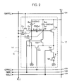
- Fig. 2 is a circuit diagram illustrating the structure of a single unit circuit.
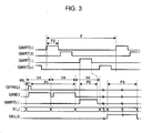
- Fig. 3 is a timing diagram for describing the operation of the electronic device.
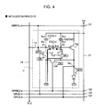
- Fig. 4 is a circuit diagram illustrating a status of the unit circuit in an initialization period.
- Fig. 5 is a circuit diagram illustrating a status of the unit circuit in a compensation period.
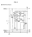
- Fig. 6 is a circuit diagram illustrating a status of the unit circuit in a data writing period.
- Fig. 7 is a circuit diagram illustrating a status of the unit circuit in a driving period.
- Fig. 8 is a circuit diagram illustrating the structure of a unit circuit according to a first modification.
- Fig. 9 is a circuit diagram illustrating the structure of a unit circuit according to a second modification.
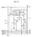
- Fig. 10 is a circuit diagram illustrating the structure of a unit circuit according to a third modification.
- Fig. 11 is a perspective view illustrating a specific form of an electronic apparatus according to one aspect of the invention.
- Fig. 12 is a perspective view illustrating another specific form of an electronic apparatus according to one aspect of the invention.
- Fig. 13 is a perspective view illustrating still another specific form of an electronic apparatus according to one aspect of the invention.
- Fig. 14 is a circuit diagram illustrating the structure of a known unit circuit.
- Fig. 1 is a block diagram illustrating the structure of an electronic apparatus according to an embodiment of the invention.
- An electronic device D illustrated in Fig. 1 is an electro-optical device (light emitting device) incorporated as an image displaying unit in one of various kinds of electronic apparatuses.
- the electronic device D includes an element array 10 having a plurality of unit circuits (pixel circuits) U arranged in a generally planer configuration.
- the electronic device D also includes a scanning-line driving circuit 22 and a data-line driving circuit 24 for driving the unit circuits U.
- Each of the scanning-line driving circuit 22 and data-line driving circuit 24 may be constructed of a transistor formed together with the element array 10 on a substrate or may be implemented in the form of an IC chip.
- the element array 10 is provided with m scanning lines 12 extending in the X direction and n data lines 14 extending in the Y direction, which is perpendicular to the X direction (m and n are each a natural number).
- Each of the unit circuits U corresponds to an intersection of each of the scanning lines 12 and each of the data lines 14. Therefore, the unit circuits U are arranged in a matrix with m rows and n columns.
- a high power supply potential Vel which is at a higher side, is supplied to each of the unit circuits U via a power supply line 17.
- the scanning-line driving circuit 22 is a circuit for successively selecting each of the plurality of scanning lines 12 in turn.
- the data-line driving circuit 24 generates data signals X[1] to X[n] corresponding to a single row of unit circuits U (i.e., n unit circuits U) connected to a scanning line 12 selected by the scanning-line driving circuit 22 and outputs the data signals to corresponding data lines 14.
- a data signal X[j] which is supplied to a j-th data line 14 (j is an integer that satisfies 1 ⁇ j ⁇ n), has a potential corresponding to a gray scale specified for a unit circuit U at the j-th column of the i-th row.
- the gray scale of each of the unit circuits U is specified by gray-scale data supplied from the exterior thereof.
- each unit circuit U includes an electro-optical element E disposed between the power supply line 17 and a low supply potential VCT.
- the electro-optical element E is a current-driven element that has a gray scale (luminance) corresponding to a drive current Iel supplied thereto.
- the electro-optical element E according to the present embodiment is an OLED element (light emitting element) in which a light emitting layer made of an organic electroluminescent (EL) material is disposed between an anode and a cathode.
- EL organic electroluminescent
- the scanning line 12 which is illustrated in Fig. 1 as a single line for the sake of convenience, actually includes four leads of a first control line 121, a second control line 122, a third control line 123, and a fourth control line 124.
- a predetermined signal is supplied from the scanning-line driving circuit 22 to each of the control lines. More specifically, a scan signal GWRT[i] is supplied to the first control line 121 included in the i-th scanning line 12.
- an initialization signal GPRE[i] is supplied to the second control line 122, a compensation control signal GINI[i] is supplied to the third control line 123, and a light-emission control signal GEL[i] is supplied to the fourth control line 124.
- GPRE[i] is supplied to the second control line 122
- a compensation control signal GINI[i] is supplied to the third control line 123
- a light-emission control signal GEL[i] is supplied to the fourth control line 124.
- a p-channel drive transistor Tdr is disposed on a path from the power supply line 17 to the anode of the electro-optical element E.
- a source (S) of the drive transistor Tdr is connected to the power supply line 17.
- the drive transistor Tdr is a unit that changes a conduction state between the source (S) and a drain (D) (resistance between the source and the drain) in response to a change in a potential of the gate (hereinafter referred to as gate potential), Vg, and thereby generates a drive current Iel corresponding to the gate potential Vg. That is, the electro-optical element E is driven in response to the conduction state of the drive transistor Tdr.
- An n-channel transistor (hereinafter referred to as light-emission control transistor) Tel that controls an electrical connection between the drain of the drive transistor Tdr and the anode of the electro-optical element E is disposed therebetween.
- a gate of the light-emission control transistor Tel is connected to the fourth control line 124. Therefore, when the light-emission control signal GEL[i] is shifted to a high level, the light-emission control transistor Tel is then changed to an on state. This enable the drive current Iel to be supplied to the electro-optical element E.
- the light-emission control transistor Tel is maintained in an off state, so the path over which the drive current Iel is to flow is being interrupted and the electro-optical element E is in the off state.
- the unit circuit U includes three capacitive elements (C1, C2, and C3) and four n-channel transistors (Tr1, Tr2, Tr3, and Tr4).
- the first capacitive element C1 is an element that has an electrode Ea1, an electrode Ea2, and a dielectric disposed in a gap between the electrodes Ea1 and Ea2 and has a capacitance value Ch1.
- the second capacitive element C2 is an element that has an electrode Eb1, an electrode Eb2, and a dielectric disposed in a gap between the electrodes Eb1 and Eb2 and has a capacitance value Ch2
- the third capacitive element C3 is an element that has an electrode Ec1, an electrode Ec2, and a dielectric disposed in a gap between the electrodes Ec1 and Ec2 and has a capacitance value Cc.
- the electrode Ea2 of the first capacitive element C1 and the electrode Eb2 of the second capacitive element C2 are connected to the power supply line 17.
- the electrode Ea1 of the first capacitive element C1 is connected to the electrode Ec1 of the third capacitive element C3.
- the electrode Eb1 of the second capacitive element C2 is connected to the electrode Ec2 of the third capacitive element C3.
- the transistor Tr1 is a switching element disposed between a node Z1 (the electrode Ec1 of the third capacitive element C3) and the data line 14 and controlling an electrical connection therebetween.
- a gate of the transistor Tr1 is connected to the first control line 121 and receives the scan signal GWRT[i].
- the transistor Tr4 is a switching element disposed between a potential line (not shown) to which an initialization potential VST is supplied and the drain of the transistor Tr4 and controlling an electrical connection therebetween.
- a gate of the transistor Tr4 is connected to the second control line 122 and receives the initialization signal GPRE[i].
- the transistor Tr2 is a switching element disposed between the node Z1 and the potential line to which the initialization potential VST is supplied and controlling an electrical connection therebetween.
- a gate of the transistor Tr2 is connected to the third control line 123 and receives the compensation control signal GINI[i].
- the transistor Tr3 is a switching element disposed between a node Z2 (the electrode Ec2 of the third capacitive element C3) and the drain of the transistor Tdr and controlling an electrical connection therebetween.
- a gate of the transistor Tr3 is connected to the third control line 123 and receives the compensation control signal GINI[i] .
- scan signals GWRT[1] to GWRT[m] are successively shifted to a high level for each predetermined period (hereinafter referred to as data writing period) P2 within each frame period F. That is, the scan signal GWRT[i] is maintained at a high level in an i-th data writing period P2 within one frame period F and maintained at a low level in the other periods within the frame period F.
- the transition of the scan signal GWRT[i] to a high level indicates that the i-th row is selected.
- the compensation control signal GINI[i] is at a high level.
- the threshold voltage Vth in the drive transistor Tdr is electrically charged by the second capacitive element C2.
- an initialization period P0 is assigned to a predetermined period before the start of the compensation period P1.
- the data writing period P2 is a period used for causing the second capacitive element C2 to hold the Vdata corresponding to a gray scale specified for a unit circuit U in responsive to gray-scale data supplied from the exterior.
- a driving period P3 the electro-optical element E is driven on the basis of the voltage held by the second capacitive element C2. Operations in the unit circuit U located in the j-th column of the i-th row will now be described below in greater detail with reference to Figs. 4 to 7 for each of the initialization period P0, the compensation period P1, the data writing period P2, and the driving period P3.
- Fig. 4 illustrates a status of the unit circuit U in an initialization period P0 where the initialization signal GPRE[i] is at a high level.
- the initialization signal GPRE[i] and the compensation control signal GINI[i] are at a high level, and therefore the transistor Tr2, the transistor Tr3, and the transistor Tr4 are in the on state.
- electrical charges stored in the electrodes Ec1 and Ec2 of the third capacitive element C3 are discharged, and the potential thereof is set at the initialization potential VST.
- the scan signal GWRT[i] and the light-emission control signal GEL[i] are at a low level, and the transistor Tr1 and the light-emission control transistor Tel are in the off state.
- Fig. 5 illustrates a status of the unit circuit U in a compensation period P1.
- the initialization signal GPRE[i] is shifted from a high level to a low level
- the compensation control signal GINI[i] is at a high level. Therefore, the transistor Tr4 is shifted from the on state to the off state, and the transistor Tr2 and the transistor Tr3 are maintained in the on state.
- the potential of the electrode Ec1 of the third capacitive element C3 is fixed at the initialization potential VST, and the drive transistor Tdr is diode-connected. A current flows from the source to the drain in the drive transistor Tdr.
- the compensation period P1 can be set in a horizontal scan period different from that in which the data writing period P2 is set. In this example, as illustrated in Fig. 3, one compensation period P1 is set across a boundary between two consecutive horizontal scan periods. As a result, variations in the threshold voltage Vth can be sufficiently compensated.
- the initialization potential VST is set at a potential smaller than a value of "Vel-Vth". Therefore, at the time of starting a compensation operation, the gate potential Vg of the drive transistor Tdr is sufficiently low. Thus, it is not necessary to decrease the gate potential Vg by feeding a current through the electro-optical element E.
- a low-level light-emission control signal GEL[i] maintains the off state of the light-emission control transistor Tel, and the drive current Iel is not supplied to the electro-optical element E. If the drive current Iel is fed through the electro-optical element E to decrease the gate potential Vg, a grayish display would appear when a black display should have appeared, thus resulting in degraded image quality. In contrast to this, in the present embodiment, since the initialization potential VST is supplied, the image quality in display can be improved.
- Fig. 6 illustrates a status of the unit circuit U in a data writing period P2 where the scan signal GWRT[i] is at a high level.
- the transistor Tr1 is changed to the on state
- the transistors Tr2 and Tr3 are changed to the off state
- the transistor Tr4 and the light-emission control transistor Tel are maintained in the off state.
- the electrode Ec1 of the third capacitive element C3 is electrically connected to the data line 14.
- a potential of VST- ⁇ Vdata is supplied as a data signal X[j] to the data line 14.
- the potential of the electrode Ec1 of the third capacitive element C3 is changed from the initialization potential VST to the potential VST- ⁇ Vdata.
- ⁇ V ⁇ 1 - ⁇ ⁇ Vdata
- Fig. 7 illustrates a status of the unit circuit U in a driving period P3.
- the scan signal GWRT[i], the initialization signal GPRE[i], and the compensation control signal GINI[i] are at a low level. Therefore, the transistor Tr1 is changed to the off state, and the electrode Ec1 of the third capacitive element C3 is electrically isolated from the data line 14.
- the transistors Tr2, Tr3, and Tr4 are in the off state.
- the light-emission control signal GEL[i] is at a high level, the light-emission control transistor Tel is changed to the on state.
- the drive current Iel according to the magnitude of the gate potential Vg is supplied from the drive transistor Tdr to the electro-optical element E.
- the drive current Iel is determined by the potential Vdata and does not depend on the threshold voltage Vth in the transistor Tdr. Therefore, variations in the threshold voltage Vth in the drive transistor Tdr in each unit circuit U can be compensated, and thus non-uniformity in gray scale (luminance) in the electro-optical elements E can be suppressed.
- the compensation period P1 and the data writing period P2 can be set in different horizontal scan periods. Therefore, each of the compensation period P1 and the data writing period P2 can be a long time period. As a result, variations in the threshold voltage Vth can be accurately compensated, and the voltage Vdata can be sufficiently written. Hence, non-uniformity in luminance can be reduced and precision in gray scale in display can be improved.
- a known unit circuit illustrated in Fig. 14 is first discussed.
- the parasitic capacitor C4 occurs between the data line L and the node Z1 and has a capacitance value Ca.
- the parasitic capacitor C5 occurs between the data line L and the node Z2 and has a capacitance value Cb.
- a comparison of expressions (17) and (18) shows that the effects of crosstalk in the unit circuit U illustrated in Fig. 2 according to the present embodiment is reduced to approximately one-third of the effects thereof illustrated in Fig. 14. Therefore, even when the potential of the data line 14 varies, the unit circuit U that is relatively immune to the effects of crosstalk can be provided.
- connecting the first capacitive element C1 to the third capacitive element C3 in a "pi" configuration such that the first capacitive element C1 and the second capacitive element C2 are provided at the nodes Z1 and Z2, respectively, can reduce crosstalk caused by a capacitance Cds between the source and drain in the transistor Tr1.
- the capacitance value Ch1 of the first capacitive element C1, the capacitance value Ch2 of the second capacitive element C2, and the capacitance value Ch3 of the third capacitive element C3 at substantially the same value can achieve the maximum magnitude of the total capacitance of each of the nodes Z1 and Z2. This can further reduce the effects of crosstalk.
- the crosstalk described above deals with between a unit circuit U and a data line 14 that supplies a data potential to this unit circuit U. Although a similar problem occurs in between the unit circuit U and a data line 14 for an adjacent unit circuit U, the use of unit circuits U according to the present embodiment can similarly reduce crosstalk caused by the data line 14 for the adjacent unit circuit U.
- Fig. 8 illustrates a unit circuit U1.
- the unit circuit U1 different signals are supplied to the gate of each of the transistors Tr2 and Tr3.
- a second compensation control signal GINI2[i] is supplied to the third control line 123
- a first compensation control signal GINI1[i] is supplied to a fifth control line 125.
- the operation of the unit circuit U1 is substantially the same as in the above-described embodiment in the initialization period P0, compensation period P1, data writing period P2, and driving period P3.
- the compensation control signal GINI1[i] and second compensation control signal GINI2[i] the compensation control signal GINI[i] described above is supplied (see Fig. 3).
- One of the inspections is to inspect a short circuit of each of the first capacitive element C1 and the third capacitive element C3.
- the scan signal GWRT[i], the first compensation control signal GINI1[i], and the initialization signal GPRE[i] are set at a high level, whereas the light-emission control signal GEL[i] and the second compensation control signal GINI2[i] are set at a low level. This causes the transistors Tr1, Tr3, and Tr4 to be in the on state. If a short circuit occurs between the electrodes Ea1 and Ea2 of the first capacitive element C1, the potential of the data line 14 is equal to the high power supply potential Vel.
- the potential of the data line 14 is equal to the initialization potential VST.
- measuring the potential of the data line 14 can detect a short circuit of each of the first capacitive element C1 and the third capacitive element C3. Therefore, according to the unit circuits U1, the inspection can be readily performed.
- Fig. 9 illustrates a unit circuit U2.
- the unit circuit U2 is substantially the same as the unit circuit U illustrated in Fig. 2 according to the embodiment, with the exception that the transistor Tr2 is disposed between a power-supply line that supplies the initialization potential VST and a first input terminal of the transistor Tr4.
- a supply of substantially the same signals as in the embodiment described above to the first control line 121 to the fourth control line 124 can cause the third capacitive element C3 to discharge charges stored therein in the initialization period P0, cause the second capacitive element C2 to hold the threshold voltage Vth in the compensation period P1, and cause the third capacitive element C3 to operate as a coupling capacitance and a potential corresponding to a data potential to be applied to the gate of the drive transistor Tdr and held thereby in the data writing period P2.
- it causes a drive current Iel corresponding to a compensated threshold voltage Vth to be supplied to the electro-optical element E in the driving period P3.
- Fig. 10 illustrates a unit circuit U3.
- the unit circuit U3 different signals are supplied to the gate of each of the transistors Tr2 and Tr3.
- the second compensation control signal GINI2[i] is supplied to the third control line 123
- the first compensation control signal GINI1 [i] is supplied to the fifth control line 125.
- the operation of the unit circuit U3 is substantially the same as in the above-described embodiment in the initialization period P0, compensation period P1, data writing period P2, and driving period P3.
- the compensation control signal GINI1[i] and second compensation control signal GINI2[i] the compensation control signal GINI[i] described above is supplied (see Fig. 3).
- the scan signal GWRT[i] is set at a high level, whereas the light-emission control signal GEL[i], the first compensation control signal GINI1[i], the second compensation control signal GINI2[i], and the initialization signal GPRE[i] are set at a low level.
- This causes the transistor Tr1 to be in the on state and the transistors Tr2, Tr3, and Tr4 to be in the off state.
- the potential of the data line 14 is equal to the high power supply potential Vel.
- measuring the potential of the data line 14 can detect a short circuit of the first capacitive element C1.
- the scan signal GWRT[i] and the light-emission control signal GEL[i] are set at a low level, whereas the first compensation control signal GINI1[i], the second compensation control signal GINI2[i], and the initialization signal GPRE[i] are set at a high level.
- This causes the transistor Tr1 and the light-emission control transistor Tel to be in the off state and the transistors Tr2, Tr3, and Tr4 to be in the on state.
- the potential of the electrodes Ea1 and Ea2 is equal to the initialization potential VST.
- the scan signal GWRT[i] and the first compensation control signal GINI1[i] are set at a high level, whereas the light-emission control signal GEL[i], the second compensation control signal GINI2[i], and the initialization signal GPRE[i] are set at a low level.
- This causes the transistors Tr1 and Tr3 to be in the on state and the light-emission control transistor Tel and the transistors Tr2 and Tr4 to be in the off state. If a short circuit occurs in the third capacitive element C3, the potential of the electrode Ec1 converges to a value of "Vel-Vth"; if a short circuit does not occur in the third capacitive element C3, the potential of the electrode Ec1 is equal to the initialization potential VST. As a result, measuring the potential of the data line 14 can detect a short circuit of the first capacitive element C1.
- a specific structure of the unit circuit U is not limited to the embodiment and modifications described above.
- the conductivity type of each transistor in the unit circuit U can be changed as appropriate.
- the light-emission control transistor Tel can be omitted as appropriate.
- an OLED element is used as the electro-optical element E by way of example.
- An electro-optical element (driven element) used in an electronic device according to an aspect of the invention is not limited to the OLED element.
- various light emitting elements such as an inorganic EL element, a field emission (FE) element, a surface-conduction electron-emitter (SE) element, a ballistic electron surface-emitting (BS) element, and a light emitting diode (LED) element
- various other electro-optical elements such as a liquid crystal element, an electrophoretic element, and electrochromic element, can be used.
- the invention is also applicable to a sensing device, such as a biochip.
- FIG. 11 to 13 illustrate applications each using an electronic device D according to at least one of the embodiment and modifications described above.
- FIG. 11 is a perspective view illustrating the structure of a mobile personal computer that uses an electronic device D according to at least one of the embodiment and modifications described above.
- a personal computer 2000 includes the electronic device D capable of displaying various images and a main body 2010 provided with a power switch 2001 and a keyboard 2002.
- the electronic device D uses an OLED element as the electro-optical element E. Therefore, the electronic device D can display an easy-to-see screen with a wide viewing angle.
- FIG. 12 illustrates the structure of a cellular phone that uses an electronic device D according to at least one of the embodiment and modifications.
- a cellular phone 3000 includes a plurality of operation buttons 3001, scroll buttons 3002, and the electronic device D capable of displaying various images. Operating the scroll buttons 3002 scrolls a screen displayed on the electronic device D.
- Fig. 13 illustrates the structure of a personal digital assistant (PDA) that uses an electronic device D according to at least one of the embodiment and modifications described above.
- a PDA terminal 4000 includes a plurality of operation buttons 4001, a power switch 4002, and the electronic device D capable of displaying various images. Operating the power switch 4002 causes the electronic device D to display various kinds of information, such as addresses and schedules.
- Examples of an electronic apparatus that uses an electronic device according to at least one of embodiment and modifications of the inventions include, in addition to apparatuses illustrated in Figs. 11 to 13, a digital still camera, a television, a video camera, a cam coder, a car navigation system, a pager, an electronic organizer, electronic paper, an electronic calculator, a word processor, a work station, a videophone, a point-of-sale (POS) terminal, a printer, a scanner, a copier, a video player, and a device having a touch panel.
- Applications of an electronic device according to the invention are not limited to image displaying.
- the electronic device according to the invention is applicable to a writing head that exposes a photosensitive member in accordance with an image to be formed on a recording medium (e.g., a sheet of paper) for use in an image forming apparatus, such as an optical writing printer and electronic copier.
- a writing head that exposes a photosensitive member in accordance with an image to be formed on a recording medium (e.g., a sheet of paper) for use in an image forming apparatus, such as an optical writing printer and electronic copier.
Landscapes
- Engineering & Computer Science (AREA)
- Physics & Mathematics (AREA)
- Computer Hardware Design (AREA)
- General Physics & Mathematics (AREA)
- Theoretical Computer Science (AREA)
- Control Of El Displays (AREA)
- Control Of Indicators Other Than Cathode Ray Tubes (AREA)
- Electroluminescent Light Sources (AREA)
Applications Claiming Priority (1)
| Application Number | Priority Date | Filing Date | Title |
|---|---|---|---|
| JP2006147741A JP4736954B2 (ja) | 2006-05-29 | 2006-05-29 | 単位回路、電気光学装置、及び電子機器 |
Publications (2)
| Publication Number | Publication Date |
|---|---|
| EP1863003A2 true EP1863003A2 (de) | 2007-12-05 |
| EP1863003A3 EP1863003A3 (de) | 2008-07-16 |
Family
ID=38372422
Family Applications (1)
| Application Number | Title | Priority Date | Filing Date |
|---|---|---|---|
| EP07010494A Withdrawn EP1863003A3 (de) | 2006-05-29 | 2007-05-25 | Einheitsschaltung, elektrooptische Vorrichtung und elektronisches Gerät |
Country Status (6)
| Country | Link |
|---|---|
| US (1) | US8072396B2 (de) |
| EP (1) | EP1863003A3 (de) |
| JP (1) | JP4736954B2 (de) |
| KR (1) | KR101313144B1 (de) |
| CN (1) | CN101093641B (de) |
| TW (1) | TWI437539B (de) |
Families Citing this family (51)
| Publication number | Priority date | Publication date | Assignee | Title |
|---|---|---|---|---|
| KR100911969B1 (ko) * | 2007-12-06 | 2009-08-13 | 삼성모바일디스플레이주식회사 | 화소 및 이를 이용한 유기전계발광 표시장치 |
| TWI383355B (zh) * | 2008-05-27 | 2013-01-21 | Univ Nat Cheng Kung | A driving circuit and a pixel circuit having the driving circuit |
| JP4816686B2 (ja) | 2008-06-06 | 2011-11-16 | ソニー株式会社 | 走査駆動回路 |
| JP5434092B2 (ja) * | 2009-01-27 | 2014-03-05 | セイコーエプソン株式会社 | 発光装置及び電子機器 |
| JP2010175779A (ja) * | 2009-01-29 | 2010-08-12 | Seiko Epson Corp | 単位回路の駆動方法及び電気光学装置の駆動方法 |
| JP5360684B2 (ja) * | 2009-04-01 | 2013-12-04 | セイコーエプソン株式会社 | 発光装置、電子機器および画素回路の駆動方法 |
| US9324465B2 (en) * | 2009-04-01 | 2016-04-26 | Ge-Hitachi Nuclear Energy Americas Llc | Methods and apparatuses for operating nuclear reactors and for determining power levels in the nuclear reactors |
| JP2010249935A (ja) * | 2009-04-13 | 2010-11-04 | Sony Corp | 表示装置 |
| KR101056281B1 (ko) * | 2009-08-03 | 2011-08-11 | 삼성모바일디스플레이주식회사 | 유기 전계발광 표시장치 및 그의 구동방법 |
| KR20110013693A (ko) | 2009-08-03 | 2011-02-10 | 삼성모바일디스플레이주식회사 | 유기 전계발광 표시장치 및 그의 구동방법 |
| KR101135534B1 (ko) * | 2010-02-10 | 2012-04-13 | 삼성모바일디스플레이주식회사 | 화소, 이를 이용한 표시 장치, 및 그들의 구동 방법 |
| KR101645404B1 (ko) | 2010-07-06 | 2016-08-04 | 삼성디스플레이 주식회사 | 유기 전계발광 표시장치 |
| KR101674479B1 (ko) * | 2010-08-10 | 2016-11-10 | 삼성디스플레이 주식회사 | 유기전계발광 표시장치 |
| KR101797161B1 (ko) * | 2010-12-23 | 2017-11-14 | 삼성디스플레이 주식회사 | 화소 및 이를 이용한 유기 발광 표시 장치 |
| KR101839533B1 (ko) | 2010-12-28 | 2018-03-19 | 삼성디스플레이 주식회사 | 유기 발광 표시 장치, 이의 구동 방법 및 그 제조 방법 |
| KR101835637B1 (ko) * | 2011-08-22 | 2018-04-20 | 에스케이하이닉스 주식회사 | 집적회로 칩 및 이를 포함하는 송/수신 시스템 |
| JP6064313B2 (ja) | 2011-10-18 | 2017-01-25 | セイコーエプソン株式会社 | 電気光学装置、電気光学装置の駆動方法および電子機器 |
| JP6141590B2 (ja) | 2011-10-18 | 2017-06-07 | セイコーエプソン株式会社 | 電気光学装置および電子機器 |
| JP2013088640A (ja) * | 2011-10-19 | 2013-05-13 | Seiko Epson Corp | 電気光学装置の駆動方法、電気光学装置および電子機器 |
| JP5853614B2 (ja) | 2011-11-10 | 2016-02-09 | セイコーエプソン株式会社 | 電気光学装置および電子機器 |
| JP5887973B2 (ja) | 2012-02-13 | 2016-03-16 | セイコーエプソン株式会社 | 電気光学装置、電気光学装置の駆動方法および電子機器 |
| JP5821685B2 (ja) | 2012-02-22 | 2015-11-24 | セイコーエプソン株式会社 | 電気光学装置および電子機器 |
| JP6056175B2 (ja) | 2012-04-03 | 2017-01-11 | セイコーエプソン株式会社 | 電気光学装置及び電子機器 |
| JP6111531B2 (ja) | 2012-04-25 | 2017-04-12 | セイコーエプソン株式会社 | 電気光学装置、電気光学装置の駆動方法および電子機器 |
| TWI462080B (zh) * | 2012-08-14 | 2014-11-21 | Au Optronics Corp | 主動式有機發光二極體電路及其操作方法 |
| KR20140081262A (ko) * | 2012-12-21 | 2014-07-01 | 삼성디스플레이 주식회사 | 화소 및 이를 이용한 유기전계발광 표시장치 |
| CN103208255B (zh) * | 2013-04-15 | 2015-05-20 | 京东方科技集团股份有限公司 | 像素电路、像素电路驱动方法及显示装置 |
| KR102022519B1 (ko) * | 2013-05-13 | 2019-09-19 | 삼성디스플레이 주식회사 | 화소 및 이를 이용한 유기전계발광 표시장치 |
| CN103413523B (zh) * | 2013-07-31 | 2015-05-27 | 京东方科技集团股份有限公司 | 一种像素电路、有机电致发光显示面板及显示装置 |
| CN104575367B (zh) * | 2013-10-15 | 2017-10-13 | 昆山工研院新型平板显示技术中心有限公司 | 一种像素电路及其驱动方法和应用 |
| KR20150138527A (ko) * | 2014-05-29 | 2015-12-10 | 삼성디스플레이 주식회사 | 화소 회로 및 이를 포함하는 전계발광 디스플레이 장치 |
| CN104103239B (zh) | 2014-06-23 | 2016-05-04 | 京东方科技集团股份有限公司 | 有机发光二极管像素电路及其驱动方法 |
| CN104282265B (zh) | 2014-09-26 | 2017-02-01 | 京东方科技集团股份有限公司 | 像素电路及其驱动方法、有机发光显示面板及显示装置 |
| KR102230928B1 (ko) * | 2014-10-13 | 2021-03-24 | 삼성디스플레이 주식회사 | 유기 발광 표시 장치 및 이의 구동 방법 |
| KR102481520B1 (ko) * | 2015-07-31 | 2022-12-27 | 삼성디스플레이 주식회사 | 화소 및 이를 포함하는 유기발광 표시장치 |
| JP2017134145A (ja) * | 2016-01-26 | 2017-08-03 | 株式会社ジャパンディスプレイ | 表示装置 |
| CN106935198B (zh) * | 2017-04-17 | 2019-04-26 | 京东方科技集团股份有限公司 | 一种像素驱动电路、其驱动方法及有机发光显示面板 |
| US10375278B2 (en) * | 2017-05-04 | 2019-08-06 | Apple Inc. | Noise cancellation |
| KR102369284B1 (ko) | 2017-06-01 | 2022-03-04 | 삼성디스플레이 주식회사 | 유기전계발광 표시장치 및 그의 구동방법 |
| CN109308872B (zh) * | 2017-07-27 | 2021-08-24 | 京东方科技集团股份有限公司 | 像素电路、显示基板 |
| US10997918B2 (en) * | 2018-03-30 | 2021-05-04 | Sharp Kabushiki Kaisha | Method for driving display device and display device |
| CN208335702U (zh) * | 2018-05-14 | 2019-01-04 | 北京京东方技术开发有限公司 | 显示面板及显示装置 |
| JP2020027270A (ja) * | 2018-08-13 | 2020-02-20 | セイコーエプソン株式会社 | 電気光学装置および電子機器 |
| JP7154122B2 (ja) * | 2018-12-20 | 2022-10-17 | エルジー ディスプレイ カンパニー リミテッド | 発光表示装置 |
| CN110111722A (zh) * | 2019-06-11 | 2019-08-09 | 惠州市华星光电技术有限公司 | 一种像素阵列 |
| CN111048043A (zh) * | 2019-11-26 | 2020-04-21 | 昆山国显光电有限公司 | Oled像素电路及显示装置 |
| CN111383590B (zh) | 2020-05-29 | 2020-10-02 | 合肥视涯技术有限公司 | 数据电流产生电路、驱动方法、驱动芯片和显示面板 |
| TWI758045B (zh) | 2020-12-30 | 2022-03-11 | 友達光電股份有限公司 | 顯示裝置 |
| JP2023050791A (ja) * | 2021-09-30 | 2023-04-11 | セイコーエプソン株式会社 | 電気光学装置、電子機器および電気光学装置の駆動方法 |
| KR20240159700A (ko) * | 2023-04-27 | 2024-11-06 | 삼성디스플레이 주식회사 | 표시 장치 |
| CN118675461A (zh) * | 2024-06-08 | 2024-09-20 | 安徽熙泰智能科技有限公司 | 像素电路及其驱动方法 |
Citations (3)
| Publication number | Priority date | Publication date | Assignee | Title |
|---|---|---|---|---|
| WO2004066249A1 (en) | 2003-01-24 | 2004-08-05 | Koninklijke Philips Electronics N.V. | Active matrix display devices |
| WO2004109640A1 (en) | 2003-06-06 | 2004-12-16 | Koninklijke Philips Electronics N.V. | Active matrix pixel drive circuit for oled display |
| US20050237283A1 (en) | 2004-04-22 | 2005-10-27 | Seiko Epson Corporation | Electronic circuit, driving method thereof, electro-optical device, and electronic apparatus |
Family Cites Families (9)
| Publication number | Priority date | Publication date | Assignee | Title |
|---|---|---|---|---|
| JP3618687B2 (ja) * | 2001-01-10 | 2005-02-09 | シャープ株式会社 | 表示装置 |
| JP3832415B2 (ja) | 2002-10-11 | 2006-10-11 | ソニー株式会社 | アクティブマトリクス型表示装置 |
| JP4059177B2 (ja) * | 2003-09-17 | 2008-03-12 | セイコーエプソン株式会社 | 電子回路、その駆動方法、電気光学装置および電子機器 |
| JP4747528B2 (ja) * | 2004-07-23 | 2011-08-17 | ソニー株式会社 | 画素回路及び表示装置 |
| KR100606416B1 (ko) * | 2004-11-17 | 2006-07-31 | 엘지.필립스 엘시디 주식회사 | 유기전계발광 다이오드의 구동 장치 및 구동방법 |
| KR100698697B1 (ko) * | 2004-12-09 | 2007-03-23 | 삼성에스디아이 주식회사 | 발광표시장치 및 그의 제조방법 |
| JP2006349794A (ja) * | 2005-06-14 | 2006-12-28 | Seiko Epson Corp | 電子回路、その駆動方法、電気光学装置および電子機器 |
| KR100703500B1 (ko) * | 2005-08-01 | 2007-04-03 | 삼성에스디아이 주식회사 | 데이터 구동회로와 이를 이용한 발광 표시장치 및 그의구동방법 |
| JP5124955B2 (ja) * | 2006-02-21 | 2013-01-23 | セイコーエプソン株式会社 | 電気光学装置、その駆動方法、および電子機器 |
-
2006
- 2006-05-29 JP JP2006147741A patent/JP4736954B2/ja active Active
-
2007
- 2007-05-17 US US11/749,907 patent/US8072396B2/en active Active
- 2007-05-25 KR KR1020070050826A patent/KR101313144B1/ko active Active
- 2007-05-25 EP EP07010494A patent/EP1863003A3/de not_active Withdrawn
- 2007-05-28 TW TW096118981A patent/TWI437539B/zh active
- 2007-05-28 CN CN2007101063686A patent/CN101093641B/zh active Active
Patent Citations (3)
| Publication number | Priority date | Publication date | Assignee | Title |
|---|---|---|---|---|
| WO2004066249A1 (en) | 2003-01-24 | 2004-08-05 | Koninklijke Philips Electronics N.V. | Active matrix display devices |
| WO2004109640A1 (en) | 2003-06-06 | 2004-12-16 | Koninklijke Philips Electronics N.V. | Active matrix pixel drive circuit for oled display |
| US20050237283A1 (en) | 2004-04-22 | 2005-10-27 | Seiko Epson Corporation | Electronic circuit, driving method thereof, electro-optical device, and electronic apparatus |
Also Published As
| Publication number | Publication date |
|---|---|
| TW200813959A (en) | 2008-03-16 |
| JP4736954B2 (ja) | 2011-07-27 |
| CN101093641B (zh) | 2011-03-09 |
| US8072396B2 (en) | 2011-12-06 |
| TWI437539B (zh) | 2014-05-11 |
| US20070273619A1 (en) | 2007-11-29 |
| JP2007316462A (ja) | 2007-12-06 |
| KR101313144B1 (ko) | 2013-09-30 |
| KR20070114641A (ko) | 2007-12-04 |
| EP1863003A3 (de) | 2008-07-16 |
| CN101093641A (zh) | 2007-12-26 |
Similar Documents
| Publication | Publication Date | Title |
|---|---|---|
| US8072396B2 (en) | Unit circuit, electro-optical device, and electronic apparatus | |
| KR101442052B1 (ko) | 전기 광학 장치 및 그것을 구비하는 전자 기기 | |
| KR101352943B1 (ko) | 전기 광학 장치 및 전자 기기 | |
| KR100724003B1 (ko) | 전자 회로, 그 구동 방법, 전기 광학 장치 및 전자 기기 | |
| US7755617B2 (en) | Electronic circuit, method for driving the same, electronic device, and electronic apparatus | |
| US8274499B2 (en) | Method for driving pixel circuit, electro-optic device, and electronic apparatus | |
| JP2009198761A (ja) | 発光装置、電子機器、およびリファレンス電圧設定方法 | |
| JP5011682B2 (ja) | 電子装置および電子機器 | |
| JP4826131B2 (ja) | 発光装置および電子機器 | |
| JP2012123399A (ja) | 電子回路の駆動方法 | |
| JP5494684B2 (ja) | 電子回路の駆動方法 | |
| JP4984520B2 (ja) | 電子回路、電子装置および電子機器 | |
| JP5124955B2 (ja) | 電気光学装置、その駆動方法、および電子機器 | |
| JP2007187779A (ja) | 電子回路、電子装置、その駆動方法および電子機器 | |
| JP2006349794A (ja) | 電子回路、その駆動方法、電気光学装置および電子機器 | |
| JP5103737B2 (ja) | 電子回路、電子装置および電子機器 |
Legal Events
| Date | Code | Title | Description |
|---|---|---|---|
| PUAI | Public reference made under article 153(3) epc to a published international application that has entered the european phase |
Free format text: ORIGINAL CODE: 0009012 |
|
| AK | Designated contracting states |
Kind code of ref document: A2 Designated state(s): AT BE BG CH CY CZ DE DK EE ES FI FR GB GR HU IE IS IT LI LT LU LV MC MT NL PL PT RO SE SI SK TR |
|
| AX | Request for extension of the european patent |
Extension state: AL BA HR MK YU |
|
| PUAL | Search report despatched |
Free format text: ORIGINAL CODE: 0009013 |
|
| AK | Designated contracting states |
Kind code of ref document: A3 Designated state(s): AT BE BG CH CY CZ DE DK EE ES FI FR GB GR HU IE IS IT LI LT LU LV MC MT NL PL PT RO SE SI SK TR |
|
| AX | Request for extension of the european patent |
Extension state: AL BA HR MK RS |
|
| 17P | Request for examination filed |
Effective date: 20080923 |
|
| 17Q | First examination report despatched |
Effective date: 20081024 |
|
| AKX | Designation fees paid |
Designated state(s): DE FR GB |
|
| STAA | Information on the status of an ep patent application or granted ep patent |
Free format text: STATUS: THE APPLICATION IS DEEMED TO BE WITHDRAWN |
|
| 18D | Application deemed to be withdrawn |
Effective date: 20110716 |