EP1860639B1 - Display device - Google Patents
Display device Download PDFInfo
- Publication number
- EP1860639B1 EP1860639B1 EP07010122.5A EP07010122A EP1860639B1 EP 1860639 B1 EP1860639 B1 EP 1860639B1 EP 07010122 A EP07010122 A EP 07010122A EP 1860639 B1 EP1860639 B1 EP 1860639B1
- Authority
- EP
- European Patent Office
- Prior art keywords
- voltage
- electrode
- gate
- storage electrode
- storage
- Prior art date
- Legal status (The legal status is an assumption and is not a legal conclusion. Google has not performed a legal analysis and makes no representation as to the accuracy of the status listed.)
- Ceased
Links
Images


Classifications
-
- G—PHYSICS
- G02—OPTICS
- G02F—OPTICAL DEVICES OR ARRANGEMENTS FOR THE CONTROL OF LIGHT BY MODIFICATION OF THE OPTICAL PROPERTIES OF THE MEDIA OF THE ELEMENTS INVOLVED THEREIN; NON-LINEAR OPTICS; FREQUENCY-CHANGING OF LIGHT; OPTICAL LOGIC ELEMENTS; OPTICAL ANALOGUE/DIGITAL CONVERTERS
- G02F1/00—Devices or arrangements for the control of the intensity, colour, phase, polarisation or direction of light arriving from an independent light source, e.g. switching, gating or modulating; Non-linear optics
- G02F1/01—Devices or arrangements for the control of the intensity, colour, phase, polarisation or direction of light arriving from an independent light source, e.g. switching, gating or modulating; Non-linear optics for the control of the intensity, phase, polarisation or colour
- G02F1/13—Devices or arrangements for the control of the intensity, colour, phase, polarisation or direction of light arriving from an independent light source, e.g. switching, gating or modulating; Non-linear optics for the control of the intensity, phase, polarisation or colour based on liquid crystals, e.g. single liquid crystal display cells
- G02F1/133—Constructional arrangements; Operation of liquid crystal cells; Circuit arrangements
-
- G—PHYSICS
- G09—EDUCATION; CRYPTOGRAPHY; DISPLAY; ADVERTISING; SEALS
- G09G—ARRANGEMENTS OR CIRCUITS FOR CONTROL OF INDICATING DEVICES USING STATIC MEANS TO PRESENT VARIABLE INFORMATION
- G09G3/00—Control arrangements or circuits, of interest only in connection with visual indicators other than cathode-ray tubes
- G09G3/20—Control arrangements or circuits, of interest only in connection with visual indicators other than cathode-ray tubes for presentation of an assembly of a number of characters, e.g. a page, by composing the assembly by combination of individual elements arranged in a matrix no fixed position being assigned to or needed to be assigned to the individual characters or partial characters
- G09G3/34—Control arrangements or circuits, of interest only in connection with visual indicators other than cathode-ray tubes for presentation of an assembly of a number of characters, e.g. a page, by composing the assembly by combination of individual elements arranged in a matrix no fixed position being assigned to or needed to be assigned to the individual characters or partial characters by control of light from an independent source
- G09G3/36—Control arrangements or circuits, of interest only in connection with visual indicators other than cathode-ray tubes for presentation of an assembly of a number of characters, e.g. a page, by composing the assembly by combination of individual elements arranged in a matrix no fixed position being assigned to or needed to be assigned to the individual characters or partial characters by control of light from an independent source using liquid crystals
- G09G3/3611—Control of matrices with row and column drivers
- G09G3/3648—Control of matrices with row and column drivers using an active matrix
- G09G3/3655—Details of drivers for counter electrodes, e.g. common electrodes for pixel capacitors or supplementary storage capacitors
-
- G—PHYSICS
- G09—EDUCATION; CRYPTOGRAPHY; DISPLAY; ADVERTISING; SEALS
- G09G—ARRANGEMENTS OR CIRCUITS FOR CONTROL OF INDICATING DEVICES USING STATIC MEANS TO PRESENT VARIABLE INFORMATION
- G09G2330/00—Aspects of power supply; Aspects of display protection and defect management
- G09G2330/02—Details of power systems and of start or stop of display operation
- G09G2330/021—Power management, e.g. power saving
Definitions
- auxiliary scan circuit (4) comprising three switches (SW1-SW3) and arranged to drive the Cs counter electrode of the storage capacitor (Cs) with a boosting voltage (COM) in time periods of a frame outside the pixel data driving period (refer for instance to figures 2B and 2C ).
- FIGs. 8A and 8B are cross-sectional views of the thin film transistor array panel taken along lines XA-XA and XB-XB of FIG. 7 , respectively;
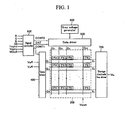
- FIG. 1 is a block diagram of a liquid crystal display according to an exemplary embodiment of the present invention
- FIG. 2 is an equivalent circuit diagram of one pixel in the liquid crystal display according to an exemplary embodiment of the present invention.
- Pixel switching element Kij is a three terminal element such as a thin film transistor, and is disposed on the lower panel 100. Pixel switching element Kij has a control terminal connected to the gate line G i , an input terminal connected to the data line D j , and an output terminal connected to the liquid crystal capacitor Clc and storage capacitor Cst.
- Signal controller 600 controls gate driver 400 and data driver 500.
- Signal controller 600 receives input image signals R, G, and B and input control signals from an external graphics controller (not shown).
- the input image signals R, G, and B contain luminance information of pixels PX.
- the input control signals include a vertical synchronization signal Vsync, a horizontal synchronization signal Hsync, a main clock signal MCLK, and a data enable signal DE.
- Signal controller 600 processes the image signals R, G, and B based on the input control signals and the input image signals R, G, and B to generate gate control signals CONT1 and data control signals CONT2, and then transmits them to corresponding drivers.
- Gate control signals CONT1 include a scanning start signal STV for indicating scanning start, and at least one clock signal for controlling an output period of the turn-on voltage Von. Gate control signals CONT1 may also include an output enable signal OE for defining the duration of the turn-on voltage Von.
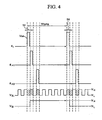
- the storage voltage is changed from a high level voltage, as a sustaining voltage, to a low level voltage, as a boosting voltage, when pixel electrode 191 is charged by a negative polarity data voltage.
- This decrease in voltage of the storage electrode decreases pixel electrode voltage by capacitive coupling.
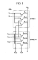
- the third transistor Qi,3 of the i_th stage STAGE_i has a source electrode as an input terminal, a drain electrode as an output terminal and a gate electrode as a control terminal.
- the source electrode of the third transistor Qi,3 is connected to the storage electrode lines driving voltage source VSL through the storage electrode lines driving voltage supplying line SL.
- the drain electrode of the third transistor Qi,3 is connected to the i_th storage electrode lines Si.
- the gate electrode of the third transistor Qi,3 is connected to the i+3_th gate line Gi+3.
- V D The sign after V D is positive(+) when the data voltage has a positive polarity, and negative(-) when the data voltage has a negative polarity.
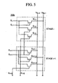
- the liquid crystal panel may include 2N+1 additional gate lines because the second transistor of the last stage needs a next gate line to be connected and each third transistor of the last 2N+1 stages needs a 2N+1th next gate line respectively.
- the gate electrode of the third transistor in the 98th, 99th and 100th stage needs a 101th, 102th and 103th gate line respectively to be connected to.
- These 101th, 102th and 103th gate lines are additional gate lines which sequentially shifted turn-on voltages are applied and are not connected to pixel transistors.
- each of the first and second voltage source generates a driving voltage alternating between a high level and a low level with an alternating period of about 2 frames.
- the phases of alternating voltages generated by these two driving voltage sources are opposite to each other.
- Each stage of the storage electrode driver includes three transistors and each transistor has a drain electrode connected to the same storage electrode lines.
- the mechanism of boosting the pixel voltage and sustaining the storage voltage by the second and third transistor is same as explained in the first embodiment.
- Each of the storage electrode linking lines 196 is connected to drain electrodes of the switching element of the storage electrode driver. At least a part of the storage electrode linking lines 196 is overlapped with the enlarged portion of the first electrode 197.
- a plurality of pixel electrodes 191, a plurality of contact bridges and at least a second electrode 198 are formed on passivation layer 180.
- Pixel electrode 191 is physically and electrically connected to drain electrode 175 through the contact hole 185, and receives a data voltage applied by drain electrode 175.
- Each storage line is connected to the second sustaining electrode through the contact holes 183, 184.
Landscapes
- Physics & Mathematics (AREA)
- Engineering & Computer Science (AREA)
- General Physics & Mathematics (AREA)
- Crystallography & Structural Chemistry (AREA)
- Chemical & Material Sciences (AREA)
- Computer Hardware Design (AREA)
- Power Engineering (AREA)
- Theoretical Computer Science (AREA)
- Nonlinear Science (AREA)
- Mathematical Physics (AREA)
- Optics & Photonics (AREA)
- Control Of Indicators Other Than Cathode Ray Tubes (AREA)
- Liquid Crystal Display Device Control (AREA)
- Liquid Crystal (AREA)
Applications Claiming Priority (1)
| Application Number | Priority Date | Filing Date | Title |
|---|---|---|---|
| KR1020060046028A KR101252002B1 (ko) | 2006-05-23 | 2006-05-23 | 액정 표시 장치 |
Publications (2)
| Publication Number | Publication Date |
|---|---|
| EP1860639A1 EP1860639A1 (en) | 2007-11-28 |
| EP1860639B1 true EP1860639B1 (en) | 2013-11-06 |
Family
ID=38358011
Family Applications (1)
| Application Number | Title | Priority Date | Filing Date |
|---|---|---|---|
| EP07010122.5A Ceased EP1860639B1 (en) | 2006-05-23 | 2007-05-22 | Display device |
Country Status (6)
| Country | Link |
|---|---|
| US (1) | US8242996B2 (enExample) |
| EP (1) | EP1860639B1 (enExample) |
| JP (1) | JP5134861B2 (enExample) |
| KR (1) | KR101252002B1 (enExample) |
| CN (1) | CN101078846A (enExample) |
| TW (1) | TWI430241B (enExample) |
Families Citing this family (12)
| Publication number | Priority date | Publication date | Assignee | Title |
|---|---|---|---|---|
| RU2438194C1 (ru) * | 2007-12-28 | 2011-12-27 | Шарп Кабусики Кайся | Схема управления линии запоминающего конденсатора и устройство отображения |
| US8718223B2 (en) | 2007-12-28 | 2014-05-06 | Sharp Kabushiki Kaisha | Semiconductor device and display device |
| CN103036548B (zh) | 2007-12-28 | 2016-01-06 | 夏普株式会社 | 半导体装置和显示装置 |
| US8547368B2 (en) | 2007-12-28 | 2013-10-01 | Sharp Kabushiki Kaisha | Display driving circuit having a memory circuit, display device, and display driving method |
| KR101499843B1 (ko) * | 2008-07-04 | 2015-03-06 | 삼성디스플레이 주식회사 | 표시장치 |
| KR101147424B1 (ko) * | 2010-03-18 | 2012-05-23 | 삼성모바일디스플레이주식회사 | 표시 장치 및 그 구동 방법 |
| US8693679B1 (en) * | 2010-07-22 | 2014-04-08 | Adtran, Inc. | Communications system and associated method for reducing power consumption of a telecommunications device |
| US8564922B1 (en) | 2010-07-22 | 2013-10-22 | Adtran, Inc. | System and method for protecting telecommunications device from power faults |
| KR101296904B1 (ko) * | 2010-12-24 | 2013-08-20 | 엘지디스플레이 주식회사 | 입체영상 표시장치 및 그 구동방법 |
| CN103761953B (zh) * | 2014-01-28 | 2016-04-06 | 北京京东方显示技术有限公司 | 一种显示控制单元及显示装置 |
| KR102396288B1 (ko) | 2014-10-27 | 2022-05-10 | 삼성디스플레이 주식회사 | 유기 발광 표시 장치 |
| CN111145677A (zh) | 2020-01-03 | 2020-05-12 | 京东方科技集团股份有限公司 | 选择电路及其控制方法以及多路复用电路 |
Family Cites Families (23)
| Publication number | Priority date | Publication date | Assignee | Title |
|---|---|---|---|---|
| JP2619055B2 (ja) * | 1989-05-02 | 1997-06-11 | 株式会社東芝 | 液晶表示装置 |
| DE69225105T2 (de) * | 1991-10-04 | 1999-01-07 | Kabushiki Kaisha Toshiba, Kawasaki, Kanagawa | Flüssigkristallanzeigegerät |
| JPH05107557A (ja) * | 1991-10-15 | 1993-04-30 | Kyocera Corp | 液晶表示装置 |
| JP3596716B2 (ja) * | 1996-06-07 | 2004-12-02 | 株式会社東芝 | アクティブマトリクス型表示装置の調整方法 |
| JP2001194685A (ja) * | 2000-01-06 | 2001-07-19 | Hitachi Ltd | 液晶表示装置 |
| JP3832240B2 (ja) * | 2000-12-22 | 2006-10-11 | セイコーエプソン株式会社 | 液晶表示装置の駆動方法 |
| US7230597B2 (en) * | 2001-07-13 | 2007-06-12 | Tpo Hong Kong Holding Limited | Active matrix array devices |
| JP4595296B2 (ja) * | 2002-09-18 | 2010-12-08 | セイコーエプソン株式会社 | 電気光学装置、電子機器及びプロジェクタ |
| JP3767582B2 (ja) * | 2003-06-24 | 2006-04-19 | セイコーエプソン株式会社 | 画像表示装置、画像表示方法及び画像表示プログラム |
| JP2005062396A (ja) * | 2003-08-11 | 2005-03-10 | Sony Corp | 表示装置及びその駆動方法 |
| JP4168270B2 (ja) * | 2003-08-11 | 2008-10-22 | ソニー株式会社 | 表示装置及びその駆動方法 |
| JP2005156764A (ja) * | 2003-11-25 | 2005-06-16 | Sanyo Electric Co Ltd | 表示装置 |
| TWI240220B (en) * | 2004-04-26 | 2005-09-21 | Chunghwa Picture Tubes Ltd | Image processing method for a TFT LCD |
| US7310079B2 (en) * | 2004-07-01 | 2007-12-18 | Himax Technologies, Inc. | Apparatus and method of charge sharing in LCD |
| JP2006047993A (ja) * | 2004-07-08 | 2006-02-16 | Sharp Corp | データ変換装置 |
| JP2006072211A (ja) * | 2004-09-06 | 2006-03-16 | Casio Comput Co Ltd | 液晶表示装置及び液晶表示装置の駆動方法 |
| JP4846217B2 (ja) * | 2004-09-17 | 2011-12-28 | 東芝モバイルディスプレイ株式会社 | 液晶表示装置 |
| JP2006113359A (ja) * | 2004-10-15 | 2006-04-27 | Rohm Co Ltd | オーバードライブ回路および表示装置 |
| KR101073204B1 (ko) * | 2004-12-31 | 2011-10-12 | 엘지디스플레이 주식회사 | 액정 표시 장치 및 그 구동방법 |
| KR101112551B1 (ko) * | 2005-02-07 | 2012-02-15 | 삼성전자주식회사 | 액정 표시 장치 및 그 구동 방법 |
| JP4442569B2 (ja) * | 2005-04-11 | 2010-03-31 | セイコーエプソン株式会社 | 電気光学装置及び電子機器 |
| US7652649B2 (en) * | 2005-06-15 | 2010-01-26 | Au Optronics Corporation | LCD device with improved optical performance |
| KR101197058B1 (ko) * | 2006-02-20 | 2012-11-06 | 삼성디스플레이 주식회사 | 표시 장치의 구동 장치 |
-
2006
- 2006-05-23 KR KR1020060046028A patent/KR101252002B1/ko not_active Expired - Fee Related
-
2007
- 2007-05-15 JP JP2007129395A patent/JP5134861B2/ja not_active Expired - Fee Related
- 2007-05-22 EP EP07010122.5A patent/EP1860639B1/en not_active Ceased
- 2007-05-23 US US11/752,578 patent/US8242996B2/en not_active Expired - Fee Related
- 2007-05-23 TW TW096118441A patent/TWI430241B/zh not_active IP Right Cessation
- 2007-05-23 CN CNA2007101048648A patent/CN101078846A/zh active Pending
Also Published As
| Publication number | Publication date |
|---|---|
| TWI430241B (zh) | 2014-03-11 |
| EP1860639A1 (en) | 2007-11-28 |
| JP5134861B2 (ja) | 2013-01-30 |
| KR101252002B1 (ko) | 2013-04-08 |
| CN101078846A (zh) | 2007-11-28 |
| TW200809755A (en) | 2008-02-16 |
| JP2007316635A (ja) | 2007-12-06 |
| US8242996B2 (en) | 2012-08-14 |
| US20070273630A1 (en) | 2007-11-29 |
| KR20070113339A (ko) | 2007-11-29 |
Similar Documents
| Publication | Publication Date | Title |
|---|---|---|
| EP1860639B1 (en) | Display device | |
| US8063860B2 (en) | Display device | |
| US7468720B2 (en) | Horizontal electric field applying type liquid crystal display device and driving method thereof | |
| US8686979B2 (en) | Display device having improved gate driver | |
| US8035634B2 (en) | Electro-optical device, driving circuit, and electronic apparatus | |
| US7705819B2 (en) | Display device | |
| US20120056558A1 (en) | Display device and electronic device using the same | |
| CN101008724A (zh) | 显示器装置和驱动设备 | |
| US8786584B2 (en) | Liquid crystal display device having output transistor having large capacitor component | |
| US7312638B2 (en) | Scanning line driving circuit, display device, and electronic apparatus | |
| CN101425280A (zh) | 液晶显示装置及其驱动方法 | |
| KR101256665B1 (ko) | 액정패널 | |
| CN101013209B (zh) | 显示装置 | |
| KR101285054B1 (ko) | 액정표시장치 | |
| US20120098807A1 (en) | Active level shift driver circuit and liquid crystal display apparatus including the same | |
| JP5136350B2 (ja) | 液晶表示装置 | |
| CN101738794A (zh) | 液晶面板 | |
| US8773342B2 (en) | Display device and storage driving circuit for driving the same | |
| EP1909256B1 (en) | Liquid crystal display and driving method therefor | |
| US20130321367A1 (en) | Display device | |
| US8508519B2 (en) | Active level shift (ALS) driver circuit, liquid crystal display device comprising the ALS driver circuit and method of driving the liquid crystal display device | |
| JP4929852B2 (ja) | 電気光学装置、駆動回路および電子機器 | |
| KR20060124158A (ko) | 액정 표시 패널 및 이를 가지는 액정 표시 장치와 이 액정표시 장치의 구동 방법 |
Legal Events
| Date | Code | Title | Description |
|---|---|---|---|
| PUAI | Public reference made under article 153(3) epc to a published international application that has entered the european phase |
Free format text: ORIGINAL CODE: 0009012 |
|
| AK | Designated contracting states |
Kind code of ref document: A1 Designated state(s): AT BE BG CH CY CZ DE DK EE ES FI FR GB GR HU IE IS IT LI LT LU LV MC MT NL PL PT RO SE SI SK TR |
|
| AX | Request for extension of the european patent |
Extension state: AL BA HR MK YU |
|
| 17P | Request for examination filed |
Effective date: 20080527 |
|
| 17Q | First examination report despatched |
Effective date: 20080626 |
|
| AKX | Designation fees paid |
Designated state(s): DE FR GB NL |
|
| RAP1 | Party data changed (applicant data changed or rights of an application transferred) |
Owner name: SAMSUNG ELECTRONICS CO., LTD. |
|
| RAP1 | Party data changed (applicant data changed or rights of an application transferred) |
Owner name: SAMSUNG DISPLAY CO., LTD. |
|
| GRAP | Despatch of communication of intention to grant a patent |
Free format text: ORIGINAL CODE: EPIDOSNIGR1 |
|
| INTG | Intention to grant announced |
Effective date: 20130814 |
|
| GRAS | Grant fee paid |
Free format text: ORIGINAL CODE: EPIDOSNIGR3 |
|
| GRAA | (expected) grant |
Free format text: ORIGINAL CODE: 0009210 |
|
| AK | Designated contracting states |
Kind code of ref document: B1 Designated state(s): DE FR GB NL |
|
| REG | Reference to a national code |
Ref country code: GB Ref legal event code: FG4D |
|
| REG | Reference to a national code |
Ref country code: DE Ref legal event code: R096 Ref document number: 602007033605 Country of ref document: DE Effective date: 20140102 |
|
| REG | Reference to a national code |
Ref country code: NL Ref legal event code: VDEP Effective date: 20131106 |
|
| PG25 | Lapsed in a contracting state [announced via postgrant information from national office to epo] |
Ref country code: NL Free format text: LAPSE BECAUSE OF FAILURE TO SUBMIT A TRANSLATION OF THE DESCRIPTION OR TO PAY THE FEE WITHIN THE PRESCRIBED TIME-LIMIT Effective date: 20131106 |
|
| REG | Reference to a national code |
Ref country code: DE Ref legal event code: R097 Ref document number: 602007033605 Country of ref document: DE |
|
| PLBE | No opposition filed within time limit |
Free format text: ORIGINAL CODE: 0009261 |
|
| STAA | Information on the status of an ep patent application or granted ep patent |
Free format text: STATUS: NO OPPOSITION FILED WITHIN TIME LIMIT |
|
| 26N | No opposition filed |
Effective date: 20140807 |
|
| REG | Reference to a national code |
Ref country code: DE Ref legal event code: R097 Ref document number: 602007033605 Country of ref document: DE Effective date: 20140807 |
|
| REG | Reference to a national code |
Ref country code: FR Ref legal event code: PLFP Year of fee payment: 10 |
|
| REG | Reference to a national code |
Ref country code: FR Ref legal event code: PLFP Year of fee payment: 11 |
|
| PGFP | Annual fee paid to national office [announced via postgrant information from national office to epo] |
Ref country code: DE Payment date: 20170420 Year of fee payment: 11 Ref country code: FR Payment date: 20170424 Year of fee payment: 11 Ref country code: GB Payment date: 20170420 Year of fee payment: 11 |
|
| REG | Reference to a national code |
Ref country code: DE Ref legal event code: R119 Ref document number: 602007033605 Country of ref document: DE |
|
| GBPC | Gb: european patent ceased through non-payment of renewal fee |
Effective date: 20180522 |
|
| PG25 | Lapsed in a contracting state [announced via postgrant information from national office to epo] |
Ref country code: GB Free format text: LAPSE BECAUSE OF NON-PAYMENT OF DUE FEES Effective date: 20180522 Ref country code: DE Free format text: LAPSE BECAUSE OF NON-PAYMENT OF DUE FEES Effective date: 20181201 Ref country code: FR Free format text: LAPSE BECAUSE OF NON-PAYMENT OF DUE FEES Effective date: 20180531 |
|
| P01 | Opt-out of the competence of the unified patent court (upc) registered |
Effective date: 20230515 |