EP1860639B1 - Display device - Google Patents
Display device Download PDFInfo
- Publication number
- EP1860639B1 EP1860639B1 EP07010122.5A EP07010122A EP1860639B1 EP 1860639 B1 EP1860639 B1 EP 1860639B1 EP 07010122 A EP07010122 A EP 07010122A EP 1860639 B1 EP1860639 B1 EP 1860639B1
- Authority
- EP
- European Patent Office
- Prior art keywords
- voltage
- electrode
- gate
- storage electrode
- storage
- Prior art date
- Legal status (The legal status is an assumption and is not a legal conclusion. Google has not performed a legal analysis and makes no representation as to the accuracy of the status listed.)
- Not-in-force
Links
Images


Classifications
-
- G—PHYSICS
- G02—OPTICS
- G02F—OPTICAL DEVICES OR ARRANGEMENTS FOR THE CONTROL OF LIGHT BY MODIFICATION OF THE OPTICAL PROPERTIES OF THE MEDIA OF THE ELEMENTS INVOLVED THEREIN; NON-LINEAR OPTICS; FREQUENCY-CHANGING OF LIGHT; OPTICAL LOGIC ELEMENTS; OPTICAL ANALOGUE/DIGITAL CONVERTERS
- G02F1/00—Devices or arrangements for the control of the intensity, colour, phase, polarisation or direction of light arriving from an independent light source, e.g. switching, gating or modulating; Non-linear optics
- G02F1/01—Devices or arrangements for the control of the intensity, colour, phase, polarisation or direction of light arriving from an independent light source, e.g. switching, gating or modulating; Non-linear optics for the control of the intensity, phase, polarisation or colour
- G02F1/13—Devices or arrangements for the control of the intensity, colour, phase, polarisation or direction of light arriving from an independent light source, e.g. switching, gating or modulating; Non-linear optics for the control of the intensity, phase, polarisation or colour based on liquid crystals, e.g. single liquid crystal display cells
- G02F1/133—Constructional arrangements; Operation of liquid crystal cells; Circuit arrangements
-
- G—PHYSICS
- G09—EDUCATION; CRYPTOGRAPHY; DISPLAY; ADVERTISING; SEALS
- G09G—ARRANGEMENTS OR CIRCUITS FOR CONTROL OF INDICATING DEVICES USING STATIC MEANS TO PRESENT VARIABLE INFORMATION
- G09G3/00—Control arrangements or circuits, of interest only in connection with visual indicators other than cathode-ray tubes
- G09G3/20—Control arrangements or circuits, of interest only in connection with visual indicators other than cathode-ray tubes for presentation of an assembly of a number of characters, e.g. a page, by composing the assembly by combination of individual elements arranged in a matrix no fixed position being assigned to or needed to be assigned to the individual characters or partial characters
- G09G3/34—Control arrangements or circuits, of interest only in connection with visual indicators other than cathode-ray tubes for presentation of an assembly of a number of characters, e.g. a page, by composing the assembly by combination of individual elements arranged in a matrix no fixed position being assigned to or needed to be assigned to the individual characters or partial characters by control of light from an independent source
- G09G3/36—Control arrangements or circuits, of interest only in connection with visual indicators other than cathode-ray tubes for presentation of an assembly of a number of characters, e.g. a page, by composing the assembly by combination of individual elements arranged in a matrix no fixed position being assigned to or needed to be assigned to the individual characters or partial characters by control of light from an independent source using liquid crystals
- G09G3/3611—Control of matrices with row and column drivers
- G09G3/3648—Control of matrices with row and column drivers using an active matrix
- G09G3/3655—Details of drivers for counter electrodes, e.g. common electrodes for pixel capacitors or supplementary storage capacitors
-
- G—PHYSICS
- G09—EDUCATION; CRYPTOGRAPHY; DISPLAY; ADVERTISING; SEALS
- G09G—ARRANGEMENTS OR CIRCUITS FOR CONTROL OF INDICATING DEVICES USING STATIC MEANS TO PRESENT VARIABLE INFORMATION
- G09G2330/00—Aspects of power supply; Aspects of display protection and defect management
- G09G2330/02—Details of power systems and of start or stop of display operation
- G09G2330/021—Power management, e.g. power saving
Definitions
- auxiliary scan circuit (4) comprising three switches (SW1-SW3) and arranged to drive the Cs counter electrode of the storage capacitor (Cs) with a boosting voltage (COM) in time periods of a frame outside the pixel data driving period (refer for instance to figures 2B and 2C ).
- FIGs. 8A and 8B are cross-sectional views of the thin film transistor array panel taken along lines XA-XA and XB-XB of FIG. 7 , respectively;
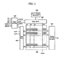
- FIG. 1 is a block diagram of a liquid crystal display according to an exemplary embodiment of the present invention
- FIG. 2 is an equivalent circuit diagram of one pixel in the liquid crystal display according to an exemplary embodiment of the present invention.
- Pixel switching element Kij is a three terminal element such as a thin film transistor, and is disposed on the lower panel 100. Pixel switching element Kij has a control terminal connected to the gate line G i , an input terminal connected to the data line D j , and an output terminal connected to the liquid crystal capacitor Clc and storage capacitor Cst.
- Signal controller 600 controls gate driver 400 and data driver 500.
- Signal controller 600 receives input image signals R, G, and B and input control signals from an external graphics controller (not shown).
- the input image signals R, G, and B contain luminance information of pixels PX.
- the input control signals include a vertical synchronization signal Vsync, a horizontal synchronization signal Hsync, a main clock signal MCLK, and a data enable signal DE.
- Signal controller 600 processes the image signals R, G, and B based on the input control signals and the input image signals R, G, and B to generate gate control signals CONT1 and data control signals CONT2, and then transmits them to corresponding drivers.
- Gate control signals CONT1 include a scanning start signal STV for indicating scanning start, and at least one clock signal for controlling an output period of the turn-on voltage Von. Gate control signals CONT1 may also include an output enable signal OE for defining the duration of the turn-on voltage Von.
- the storage voltage is changed from a high level voltage, as a sustaining voltage, to a low level voltage, as a boosting voltage, when pixel electrode 191 is charged by a negative polarity data voltage.
- This decrease in voltage of the storage electrode decreases pixel electrode voltage by capacitive coupling.
- the third transistor Qi,3 of the i_th stage STAGE_i has a source electrode as an input terminal, a drain electrode as an output terminal and a gate electrode as a control terminal.
- the source electrode of the third transistor Qi,3 is connected to the storage electrode lines driving voltage source VSL through the storage electrode lines driving voltage supplying line SL.
- the drain electrode of the third transistor Qi,3 is connected to the i_th storage electrode lines Si.
- the gate electrode of the third transistor Qi,3 is connected to the i+3_th gate line Gi+3.
- V D The sign after V D is positive(+) when the data voltage has a positive polarity, and negative(-) when the data voltage has a negative polarity.
- the liquid crystal panel may include 2N+1 additional gate lines because the second transistor of the last stage needs a next gate line to be connected and each third transistor of the last 2N+1 stages needs a 2N+1th next gate line respectively.
- the gate electrode of the third transistor in the 98th, 99th and 100th stage needs a 101th, 102th and 103th gate line respectively to be connected to.
- These 101th, 102th and 103th gate lines are additional gate lines which sequentially shifted turn-on voltages are applied and are not connected to pixel transistors.
- each of the first and second voltage source generates a driving voltage alternating between a high level and a low level with an alternating period of about 2 frames.
- the phases of alternating voltages generated by these two driving voltage sources are opposite to each other.
- Each stage of the storage electrode driver includes three transistors and each transistor has a drain electrode connected to the same storage electrode lines.
- the mechanism of boosting the pixel voltage and sustaining the storage voltage by the second and third transistor is same as explained in the first embodiment.
- Each of the storage electrode linking lines 196 is connected to drain electrodes of the switching element of the storage electrode driver. At least a part of the storage electrode linking lines 196 is overlapped with the enlarged portion of the first electrode 197.
- a plurality of pixel electrodes 191, a plurality of contact bridges and at least a second electrode 198 are formed on passivation layer 180.
- Pixel electrode 191 is physically and electrically connected to drain electrode 175 through the contact hole 185, and receives a data voltage applied by drain electrode 175.
- Each storage line is connected to the second sustaining electrode through the contact holes 183, 184.
Description
- The present invention relates to a display device.
- In general, a liquid crystal display includes two display panels having pixel electrodes, a common electrode, and a liquid crystal layer having dielectric anisotropy between the panels. The pixel electrodes are arranged in a matrix and connected to switching devices such as thin film transistors (TFTs) which sequentially apply data voltages to the pixels. The common electrode is disposed over the entire surface of the display panel and supplied with a common voltage. The pixel electrode, the common electrode, and the liquid crystal layer constitute a liquid crystal capacitor. The liquid crystal capacitor together with the switching element is a pixel unit.
- The image data voltages vary the strength of the electric field applied to the liquid crystal layer between the two panels thereby controlling the transmittance of light passing through the liquid crystal layer to display images corresponding to the data voltages. To prevent the degradation of the liquid crystal, the polarities of the data voltages with respect to the common voltage are inverted for each frame, pixel row, or pixel.
- However, since the response speed of the liquid crystal molecules is low, it takes time for a voltage (hereinafter referred to as a pixel voltage) charged in the liquid crystal capacitor to reach the target voltage. The target voltage is the voltage that effects a desired luminance. The time depends on the difference between the target voltage and the voltage previously charged on the liquid crystal capacitor. Therefore, when the difference between the target voltage and the previously-charged voltage is large, application of only the target voltage will not be enough to cause the pixel voltage to reach the target voltage during the time when the switching element is turned on.
- In order to solve the problem, a DCC (dynamic capacitance compensation) scheme has been proposed. The DCC scheme employs the fact that charging speed is proportional to the voltage across the liquid crystal capacitor. The data voltage (actually the difference between the data voltage and the common voltage, usually assumed to be 0V), applied to the pixel is chosen to be higher than the target voltage so as to shorten the time taken for the pixel voltage to reach the target voltage. However, in the DCC scheme, frame memories and driving circuits for performing DCC calculation are needed. Therefore, there are difficult problems in circuit design and increased production cost.
- To reduce power consumption in display devices of medium or small size, such as mobile phones, row inversion is performed. However, as the resolution of medium or small size display devices increases, so does power consumption. In particular, when the DCC calculation is performed, power consumption is greatly increased due to the additional calculations and circuitry.
- The range of data voltage available for image display using row inversion is small in comparison with dot inversion where the polarities of the data voltages are inverted for each pixel. Therefore, in a VA (vertical alignment) mode liquid crystal display, if the threshold voltage for driving the liquid crystal is high, the available range of the data voltage to represent grayscales for image display is reduced by the amount of the threshold voltage. Therefore, the desired luminance cannot be obtained.
- Document
US2005/0035938 discloses an auxiliary scan circuit (4) comprising three switches (SW1-SW3) and arranged to drive the Cs counter electrode of the storage capacitor (Cs) with a boosting voltage (COM) in time periods of a frame outside the pixel data driving period (refer for instance tofigures 2B and 2C ). - The present invention discloses a display device according to claims 1-13, which offers improved response speed and image quality without increasing power consumption.
- An exemplary embodiment of the present invention will be described in detail with reference to the accompanying drawing, in which:
-
FIG. 1 is a block diagram of a liquid crystal display according to an exemplary embodiment of the present invention; -
FIG. 2 is an equivalent circuit diagram of one pixel in the liquid crystal display according to an exemplary embodiment of the present invention; -
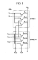
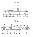
FIG. 3 is a circuit diagram of an example of a storage electrode driver according to an exemplary embodiment of the present invention; -
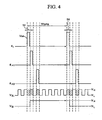
FIG. 4 is a timing diagram of signals used in the liquid crystal display including the signal generating circuit shown inFIG. 3 ; -
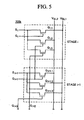
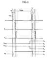
FIG. 5 is a circuit diagram of an example of a storage electrode driver not forming part of the present invention; -
FIG. 6 is a timing diagram of signals used in the liquid crystal display including the signal generating circuit shown inFIG. 5 ; -
FIG. 7 is a layout view of an example of a liquid crystal display according to embodiments of the present invention; -
FIGs. 8A and 8B are cross-sectional views of the thin film transistor array panel taken along lines XA-XA and XB-XB ofFIG. 7 , respectively; - In the drawings, the thickness of layers, films, panels, regions, etc., are exaggerated for clarity. It will be understood that when an element such as a layer, film, region, or substrate is referred to as being "on" another element, it can be directly on the other element or intervening elements may also be present. In contrast, when an element is referred to as being "directly on" another element, there are no intervening elements present. A liquid crystal display according to an exemplary embodiment of the present invention will be described in detail with reference to
FIGs. 1 and2 . -
FIG. 1 is a block diagram of a liquid crystal display according to an exemplary embodiment of the present invention, andFIG. 2 is an equivalent circuit diagram of one pixel in the liquid crystal display according to an exemplary embodiment of the present invention. - As shown in
FIG. 1 , the liquid crystal display includes a liquidcrystal panel assembly 300, agate driver 400, adata driver 500, astorage electrode driver 700, agray voltage generator 800 connected to thedata driver 500, and asignal controller 600 that controls these components. - The liquid
crystal panel assembly 300 includes a plurality of signal lines G1-Gn, D1-Dm, and S1-Sn, and a plurality of pixels PX connected to the signal lines G1-GnD1-Dm, and S1-Sn and arranged substantially in a matrix. In the structural view shown inFIG. 2 , the liquidcrystal panel assembly 300 includes lower andupper panels liquid crystal layer 3 interposed between thepanels - The storage electrode lines S1-Sn are connected to the storage electrode driver and extend substantially in the same direction as the gate lines extend.
- Referring to
Fig. 2 , each pixel PX, for example a pixel PX connected to the i-th gate line Gi Gi (i=1, 2, ..., 2n) and the j-th data line Dj (j=1, 2, ..., m), includes a pixel switching element Kij connected to the signal lines Gi and Dj, and a liquid crystal capacitor Clc and a storage capacitor Cst that are connected to the pixel switching element Kij . - Pixel switching element Kij is a three terminal element such as a thin film transistor, and is disposed on the
lower panel 100. Pixel switching element Kij has a control terminal connected to the gate line Gi, an input terminal connected to the data line Dj, and an output terminal connected to the liquid crystal capacitor Clc and storage capacitor Cst. - Liquid crystal capacitor Clc comprises
pixel electrode 191 of thelower panel 100 andcommon electrode 270 of theupper panel 200 as two electrodes, andliquid crystal layer 3 interposed between the two electrodes as a dielectric.Pixel electrode 191 is connected to pixel switching element Kij.Common electrode 270 is disposed on the entire surface of theupper panel 200 and supplied with a common voltage Vcom which is a DC voltage having a predetermined value. - The
common electrode 270 may be disposed on thelower panel 100. - Storage capacitor Cst is constructed by overlapping of
pixel electrode 191 and storage electrode lines Si with an insulator between them. - Referring to
FIG. 1 ,gray voltage generator 800 generates gate voltages and a certain number of gray voltages (referred to as "reference gray voltages" hereinafter) related to the transmittance of the pixels PX. -
Gate driver 400 generates gate signals and outputs the gate signals to the gate lines. Each of the gate signals has a turn-on voltage Von and a turn-off voltage Voff. -
Gate driver 400 may be integrated into the liquidcrystal panel assembly 300 along with the signal lines G1-Gn, D1-Dm, and S1-Sn, the switching elements Q and pixel electrodes. Alternatively,gate driver 400 may include at least one integrated circuit (IC) chip mounted on theLC panel assembly 300 or on a flexible printed circuit (FPC) film in a tape carrier package (TCP) type, which are attached to thepanel assembly 300. -
Signal controller 600controls gate driver 400 anddata driver 500.Signal controller 600 receives input image signals R, G, and B and input control signals from an external graphics controller (not shown). The input image signals R, G, and B contain luminance information of pixels PX. The luminance has a predetermined number of gray levels, for example 1024 (=210), 256 (=28), or 64 (=26) grays. The input control signals include a vertical synchronization signal Vsync, a horizontal synchronization signal Hsync, a main clock signal MCLK, and a data enable signal DE. -
Signal controller 600 processes the image signals R, G, and B based on the input control signals and the input image signals R, G, and B to generate gate control signals CONT1 and data control signals CONT2, and then transmits them to corresponding drivers. - Gate control signals CONT1 include a scanning start signal STV for indicating scanning start, and at least one clock signal for controlling an output period of the turn-on voltage Von. Gate control signals CONT1 may also include an output enable signal OE for defining the duration of the turn-on voltage Von.
- Data control signals CONT2 include a horizontal synchronization start signal STH for indicating data transmission for a row of pixels PX, a load signal LOAD for commanding to apply data voltages to the data lines D1 to Dm, and a data clock signal HCLK. Data control signals CONT2 may further include an inversion signal RVS for inverting a polarity of the data voltages with respect to the common voltage Vcom.
- In response to the data control signals CONT2 from
signal controller 600,data driver 500 receives a packet of the digital image signals DAT for a row of the pixels PX, converts the digital image signals DAT to analog data voltages selected from the gray voltages, and applies the analog data voltages to data lines D1 to Dm. -
Gate driver 400 applies the turn-on voltage Von to gate lines G1-Gn, line by line, in response to the gate control signals CONT1 from thesignal controller 600, and turns on the switching elements Q connected to a gate line in which a turn-on voltage Von is applied. - The data voltages applied to the data lines D1-Dm are then supplied to the pixels PX through the turned on switching transistors Q so that the liquid crystal capacitor Clc and storage capacitor Cst in the pixels PX are charged.
- Storage electrode driver700 is connected to storage electrode lines S1-Sn and applies a storage voltage. The storage voltage has two levels, one of the two levels is a low level and the other is a high level.
-
Storage electrode driver 700 may be integrated on the liquidcrystal panel assembly 300 along with the signal lines G1-Gn, D1-Dm, and S1-Sn, switching elements Kij and pixel electrodes. Thestorage electrode driver 700 also may be an integrated circuit (IC) chip mounted on theLC panel assembly 300 or on a flexible printed circuit (FPC) film which are attached to thepanel assembly 300. -
Storage electrode driver 700 supplies one of high or low level voltage, as a sustaining voltage, as the turn-on voltage is being applied to a gate line Gi to a storage electrode line Si overlaped with a pixel row connected to the gate line. Meanwhile the other voltage level, as a boosting voltage, at more than two different interval during the turn-off voltage is applied to said gate line to the storage electrode line Si. - Thereby, the voltage of floated
pixel electrodes 191 in the i_th pixel row is varied in accordance with the voltage variation of the storage electrode lines. By repeating this procedure for all pixel rows, the liquid crystal display displays an image for a frame. - The data voltage is selected from one of a first voltage group and second data voltage group. Data voltages of the first data voltage group are determined so that the voltage of the pixel electrode is higher than the common voltage when the boosting voltage is applied to the storage electrode line. When the data voltage is selected from the first data voltage group, the data voltage is said to have a positive polarity.
- On the other hand, data voltages of the second data voltage group are determined so that the voltage of the pixel electrode is lower than the common voltage when the boosting voltage is applied to the storage electrode line. When the data voltage is selected from the second data voltage group, the data voltage is said to have a positive polarity.
- When the next frame starts, the inversion signal RVS applied to the
data driver 500 is controlled such that the polarity of the data voltages is reversed (which is referred to as "frame inversion"). In addition, the polarity of the data voltages applied to pixels PX of a row is substantially the same while the polarity of the data voltages applied to pixels PX of the two adjacent rows is opposite (so called "row inversion"). - Since the liquid crystal display according to an exemplary embodiment of the present invention performs frame inversion and row inversion, the polarity of all data voltages applied to pixels PX of one row is positive or negative and is changed every frame.
- The storage voltage applied to storage electrode lines S1-Sn is changed from a low level voltage, as a sustaining voltage, to a high level voltage, as a boosting voltage, when
pixel electrode 191 is charged by a positive polarity data voltage. In this moment, the pixel electrode is electrically floated, so that the increase of the voltage of the storage electrode increases the pixel electrode voltage by a capacitive coupling between the storage electrode and the pixel electrode. - On the other hand, the storage voltage is changed from a high level voltage, as a sustaining voltage, to a low level voltage, as a boosting voltage, when
pixel electrode 191 is charged by a negative polarity data voltage. This decrease in voltage of the storage electrode decreases pixel electrode voltage by capacitive coupling. - Thereby, the voltage range of
pixel electrode 191 can be wider than the range of the gray voltages that are the basis of data voltages such that the luminance range using a low basic voltage is increased. - The difference between the magnitude of a pixel electrode voltage and the common voltage Vcom applied to a pixel PX is represented as a voltage across the liquid crystal capacitor Clc of the pixel PX, which is referred to as a pixel voltage. The liquid crystal molecules in the liquid crystal capacitor Clc have orientations depending on the magnitude of the pixel voltage, and the molecular orientations determine the polarization of light passing through the
liquid crystal layer 3. The polarizer(s) converts light polarization to light transmittance such that the pixel PX has a luminance represented by a gray of the data voltage. - An embodiment of the storage electrode driver according to the present invention will be explained referring to
Fig.3 and4 . -
FIG. 3 is a circuit diagram of a storage electrode driver according to an exemplary embodiment of the present invention, andFIG. 4 shows timing diagram signals used in a liquid crystal display including the storage electrode driver shown inFIG. 3 . - A storage electrode driver has a plurality of stages, each of which is connected to a strage electrode line. The i_th stage and the i+1_th stage are depicted as STAGE_i and STAGE_i+1 respectively in
Fig. 3 . - Each stage includes three or more switching devices. As one of the simplest embodiment,
Fig. 3 shows a stage having three transistors as switching devices. - The first transistor Qi,1 of the i_th stage STAGE_i has a source electrode as an input terminal, a drain electrode as an output terminal and a gate electrode as a control terminal. The source electrode of the first transistor Qi,1 is connected to the storage electrode lines driving voltage source VSL through the storage electrode lines driving voltage supply line SL. The drain electrode of the first transistor Qi,1 is connected to the i_th storage electrode lines Si. The gate electrode of the first transistor Qi,1 is connected to the i_th gate line Gi.
- The second transistor Qi,2 of the i_th stage STAGE_i has a source electrode as an inpul terminal, a drain electrode as an output terminal and a gate electrode as a control terminal. The source electrode of the second transistor Qi,2 is connected to the storage electrode lines driving voltage source VSL through the storage electrode lines driving voltage supplying line SL. The drain electrode of the second transistor Qi,2 is connected to the i_th storage electrode lines Si. And the gate electrode of the second transistor Qi,2 is connected to the i+1_th gate
line Gi+ 1. - The third transistor Qi,3 of the i_th stage STAGE_i has a source electrode as an input terminal, a drain electrode as an output terminal and a gate electrode as a control terminal. The source electrode of the third transistor Qi,3 is connected to the storage electrode lines driving voltage source VSL through the storage electrode lines driving voltage supplying line SL. The drain electrode of the third transistor Qi,3 is connected to the i_th storage electrode lines Si. The gate electrode of the third transistor Qi,3 is connected to the i+3_th gate
line Gi+ 3. - As shown in
Fig.4 , the storage driving voltage VSL alternates between high level voltage VH and low level voltage VL. The alternating period is about 2H, and the duration of each voltage level is substantially the same, in other word about 1H for each. - Referring to
Fig.3 andFig.4 , the polarity of data voltages applied to pixels connected to the i_th gate line is positive when the turn-on level Von is applied to the i_th gate line. - Simultaneously, the first transistor Qi,1 is turned on and supplies the low level VL with the storage electrode lines Si.
- After about 1H elapses, voltage applied to the i_th gate line Gi is changed to turned-off level Voff and the voltage applied to the i+1_th gate line Gi+1 is changed to turn-on level Von.
- At the same time, the second transistor Qi,2 is turned on by the Von of i+1_th gate line and supplies the high level VH with the i_th storage electrode lines Si.
- Therefore, the voltage of the i_th storage electrode line is changed from VL to VH, which changes voltages of pixels connected to the i_th gate line Gi by a capacitive coupling between the i_th storage electrode line and the pixel electrodes connected to the i_th gate line.
- On the other hand, as shown in
Fig.4 , the polarity of data voltage VD is changed to a negative in the next frame and the storage electrode lines driving voltage is a high level VH during the turn-on period of the i_th gate line Gi. The storage driving voltage VSL is changed from VL to VH when the voltage of i+1_th gate line Gi+1 changes from Voff to Von. -
Equation 1 shows the relation between the pixel voltage change and the storage electrode lines voltage. Herein, VD is the data voltage charged to the pixels connected to the i_th gate line Gi during the turn-on period of the i_th gate line Gi. -

- The sign after VD is positive(+) when the data voltage has a positive polarity, and negative(-) when the data voltage has a negative polarity.
- The range of data voltages VD can be selected according to the characteristics of the LC panel. As an embodiment, a data voltage VD is selected from a voltage set having a voltage range, for example having 5V for a maximum gray scale level and 0V for a minimum gray scale level, during the positive polarity period. The data voltage VD is selected from a voltage set having a reverse sequence of the voltage set for positive polarity, for example 0V for a maximum gray scale level and 5V for a minimum gray scale level, during the negative polarity period. In this case, a difference between the data voltage for a gray scale level and that for a maximum or minimum gray scale level is substantially same whichever the polarity is. In the above example, if a data voltage of 125th gray scale level is 3V for positive polarity and 2V for negative polarity, the difference data voltage from maximum gray scale level for each polarity is the same, 2V.
- Even though the gate electrode of a second transistor in the i_th stage is connected to the next stage, i+1_th stage, in this embodiment, the connection may be constructed differently by when the level of the storage driving voltage supplied by the second transistor is different from that supplied by the first transistor.
- One possible modification is that the gate electrode of a second transistor in the i_th stage is connected to the i+2K+1th gate line because the the level of storage driving voltage applied by turning on the second TFT is different from the level of the storage driving voltage applied by turning on the first transistor.
- Herein K is a natural number or zero. In the case that K is 0, the gate electrode of the second transistor is connected to the next gate line, for each stage.
- The second transistor Qi,2 has a parasitic capacitance between the drain electrode and the gate electrode thereof. This parasitic capacitance induces and charges the turn-on voltage to the drain electrode while the second transistor Qi,2 is turned on these induced charges flow to the storage electrode so as to drop the pixel voltage when the second transistor Qi,2 is turned off. The quantity of the pixel voltage drop is proportional to the the parasitic capacitance. Therefore it is required to reduce the parasitic capacitance for reducing the storage voltage drop.
- On the other hand, the size of the second transistor needs to be large enough to drive a whole storage capacitor line, which is a limit of reducing the parasitic capacitance.
- To solve this problem, the storage electrode driver of the present invention provides the storage driving voltage more than two times after charging pixels.
- The third transistor Qi,3 is turned on and supplies a high level VH with the i_th storage electrode lines once again when Von is applied to the i+3_th gate line.
- Therefore, the size of each transistor of the second and third transistor can be reduced because the boosting voltage supplying duration is doubled.
- The liquid crystal panel may include 2N+1 additional gate lines because the second transistor of the last stage needs a next gate line to be connected and each third transistor of the last 2N+1 stages needs a 2N+1th next gate line respectively.
- For example, when the liquid crystal has 100 gate lines and 100 storage electrode lines s, and N is 1, the gate electrode of the third transistor in the 98th, 99th and 100th stage needs a 101th, 102th and 103th gate line respectively to be connected to. These 101th, 102th and 103th gate lines are additional gate lines which sequentially shifted turn-on voltages are applied and are not connected to pixel transistors.
- Instead of forming additional gate lines on the liquid crystal panel, output terminals outputting sequentially shifted turn-on signals can be connected to the gate electrode of the third transistors of the last 2N+1 stages.
- Even though the embodiment disclosed above has only a third transistor, each stage may include additional transistor(s) with the storage electrode lines to supply enough charges with a storage electrode line.
- In this case, the the level of storage driving voltage applied by the turning-on of the additional TFT is to be same with the level of storage driving voltage applied by the turning-on of the third transistor when the additional transistor(s) must be turned on.
- For example, each stage of the storage electrode driver can include a forth transistor having a source electrode connected to the storage driving voltage source, a drain electrode connected to the storage electrode lines and a gate electrode connected to the i+5_th gate line Gi+5.
- Because the storage driving voltage alternates with about 2H period, the storage voltage is high level VH, which is the same level as when the third transistor is turned on, when the turn-on level is appliend to the i+5_th gate line.
- Moreover, each stage of the storage electrode driver can include a fifth transistor having a source electrode connected to the storage driving voltage source, a drain electrode connected to the storage electrode lines and a gate electrode connected to the i+7th gate line Gi+7, and so on.
- In general, the gate electrode of the third transistor of the i_th stage can be connected to an i+2N+1th gate line and the gate electrode of an additional transistor other than the basic three transistors Qi1, Qi,2, Qi,3 can be connected to i+2M+1th gate line, for the first embodiment described above. Herein N is a natural number larger than K and M is a natural number larger than N.
- An example of the
storage electrode driver 700 not forming part of the present invention will be explained referring toFig.5 and6 . - The storage electrode line driver includes a first driving voltage source VSL1 and a second driving voltage source VSL2.
- As shown in
Fig.6 , each of the first and second voltage source generates a driving voltage alternating between a high level and a low level with an alternating period of about 2 frames. The phases of alternating voltages generated by these two driving voltage sources are opposite to each other. - Each stage of the storage electrode driver includes three transistors and each transistor has a drain electrode connected to the same storage electrode lines.
- For a stage, the source electrode of the first transistor is connected one of the first and second driving voltage sources, and the source electrodes of second and third transistors are connected to the other of the first and second driving voltage sources.
- On the other hand, the source electrode of the first transistor in one of two neighboring stages is connected to one of the first and second driving voltage sources and the source electrode of the first transistor in the other stage is connected to the other driving voltage source.
- The structure described above will be explained referring
Fig.5 as an example. - Each of three transistors Q'i,1, Q'i,2 and Q'i,3 of the i_th stage is connected to the i_th storage line.
- The first transistor Q'i,1 has a gate electrode connected to the i_th gate line and a source electrode connected to the first driving voltage source VSL1.
- The second transistor Q'i,2 has a gate electrode connected to the i+1_th gate line and a source electrode connected to the second driving voltage source VSL2.
- The third transistor Q'i,3 has a gate electrode connected to the i+2_th gate line and a source electrode connected to the second driving voltage source VSL2·
- Each of three transistors Q'i,1, Q'i,2 and Q'i,3 of the i+1_th stage is connected to the i+1_th storage line.
- The first
transistor Q'i+ - The second
transistor Q'i+ - The third
transistor Q'i+ - When the i_th gate line is turned-on, the first transistor is turned on and supplies driving voltage generated from the first driving voltage source VSL1, which is low level, with the i_th storage electrode lines simultaneously.
- When about 1H elapses, the i_th gate line is turned-off, and the i+1_th gate line is turned-on. Therefore, the the second transistor is turned on and supplies a driving voltage generated from the second driving voltage source VSL2, which is a high level, with the i_th storage electrode lines.
- When about 1H elapses again, the i+1_th gate line is turned-off, and the i+2_th gate line is turned-on. Therefore, the the third transistor is turned on and supplies a driving voltage generated from the second driving voltage source VSL2, which is the high level, with the i_th storage electrode lines.
- The mechanism of boosting the pixel voltage and sustaining the storage voltage by the second and third transistor is same as explained in the first embodiment.
- Each stage may include additional transistor(s) as explained in the first embodiment.
- Generally, the gate electrode of the second transistor of the i_th stage can be connected to an i+Kth gate line. The gate electrode of the third transistor of the i_th stage can be connected to an i+Nth gate line, and the gate electrode of the additional transistor other than the basic three transistors Qi1, Qi,2, Qi,3 can be connected to an i+Mth gate line, for the second embodiment. Herein K is a natural number, N is a natural number larger than K and M is a natural number larger than N.
- The liquid crystal panel may include N additional gate lines because each third transistor of the last N stages needs an Nth next gate line respectively.
- For example, when the liquid crystal has 100 gate lines and 100 storage electrode lines s, and N is 2, the gate electrode of the third transistor in the 99th and 100th stage needs a 101th and 102th gate line respectively to be connected to. These 101th and 102th gate lines are additional gate lines in which sequentially shifted turn-on voltages are applied and are not connected to pixel transistors.
- Instead of forming additional gate line on the liquid crystal panel, output terminals outputting sequentially shifted turn-on signals can be connected to the gate electrode of the third transistors of the last N stages.
- Each stage of the storage electrode driver can be formed on the liquid crystal panel.
Fig.7 is a plane view of an array on the liquid crystal panel, andFig.8A and 8B are cross sectional views along XA-XA and XB-XB ofFig.7 respectively. - A plurality of
gate lines 121 and a plurality ofstorage electrode lines 131 and at least afirst electrode line 197 are disposed on an insulatingsubstrate 110 made of transparent glass or plastic. -
Gate lines 121 include agate electrode 124 that protrudes fromgate line 121, and end portions 129 that have wide surface areas for connection to other layers or an external driving circuit. - Each of the
storage electrode lines 131 includes a plurality ofenlarged portions 137. - A
first electrode line 197 primarily extends in the direction intersecting the gate line and includes a plurality of enlarged portions 197a. - A
gate insulating layer 140 is formed on thegate lines 121, the storage electrode lines s 131 and the first sustainingelectrode line 197. - A plurality of
semiconductor layers 151 are formed on thegate insulating film 140. - A plurality of line-shaped and island-shaped
ohmic contacts ohmic contacts - A plurality of
data lines 171, a plurality ofdrain electrodes 175 and a plurality of storageelectrode linking lines 196 are formed on theohmic contacts gate insulating film 140 respectively. - Each of the storage
electrode linking lines 196 is connected to drain electrodes of the switching element of the storage electrode driver. At least a part of the storageelectrode linking lines 196 is overlapped with the enlarged portion of thefirst electrode 197. - A
passivation layer 180 is formed on the substrate.Passivation layer 180 may be made of an inorganic or organic insulating material and have a planarized surface. The insulating material, there may be a silicon nitride and a silicon oxide. The organic insulating material may have photosensitivity; and the dielectric constant thereof is preferably about 4.0 or less. Alternatively,passivation layer 180 may have a double-layered structure of a lower inorganic layer and an upper organic layer in order to sustain an excellent insulating property of the organic layer and protect the exposed portions of thesemiconductor layer 151. - A plurality of contact holes 182, 183 and 185 that expose end portions of
data lines 171,drain electrodes 175 and second sustaining electrode respectively, are formed onpassivation layer 180. A plurality ofcontact holes passivation layer 180 and thegate insulating layer 140. - A plurality of
pixel electrodes 191, a plurality of contact bridges and at least asecond electrode 198 are formed onpassivation layer 180. -
Pixel electrode 191 is physically and electrically connected to drainelectrode 175 through thecontact hole 185, and receives a data voltage applied bydrain electrode 175. - Each storage line is connected to the second sustaining electrode through the contact holes 183, 184.
- The
second electrode 198 is connected to thefirst electrode 197 through thecontact hole 181, and overlapped with the second sustaining electrode. - A first capacitance is formed between the storage
electrode linking lines 196 and thefirst electrode 197 and a second capacitance is formed between the storageelectrode linking lines 196 and thesecond electrode 198. These two capacitances sustain the storage electrode voltage after the last driving voltage is applied. - While this invention has been described in connection with what is presently considered to be practical exemplary embodiments, it is to be understood by those ordinarily skilled in the art that the invention is not limited to the disclosed embodiments, but, on the contrary, is intended to cover various modifications included within the scope of the appended claims.
Claims (13)
- A display apparatus comprising:a pixel electrode (191);a data driver (500) arranged to generate a data voltage;a gate driver (400) arranged to generate a gate voltage;a pixel switching device arranged to be turned on and off according to the gate voltage, and to supply the data voltage to the pixel electrode (191) when being turned on;a storage capacitor (Cst) comprising a part of the pixel electrode (191), a storage electrode and a insulator therebetween; anda storage electrode driver (700) arranged to supply a boosting voltage to the storage electrode for at least two time periods in a frame while the pixel switching device is turned off;wherein the storage electrode driver (700) comprises
a voltage source (VSL) being arranged to supply a storage voltage supply line with a storage electrode voltage alternating between a first level (VL) and a second level (VH) higher than the first level (VL) at an alternating cycle;
a stage (STAGE i, STAGE i+1) comprising;
a first switching element (Qi.1; Qi+1.1) comprising an output terminal connected to the storage electrode, an input terminal connected to the storage voltage supply line and a control terminal connected to a first control signal source;
a second switching element (Qi.2; Qi+1.2) comprising an output terminal connected to the storage electrode,
an input terminal connected to the storage voltage supply line and a control terminal connected to a second control signal source; and
a third switching element (Qi.3; Qi+1.3) comprising an output terminal connected to the storage electrode, an input terminal connected to the storage voltage supply line and a control terminal connected to a third control signal source;the display apparatus further comprising a plurality of gate lines (G1-Gn) connected to the gate driver (400);the gate driver (400) being arranged to supply each of the plurality of gate lines (G1-Gn) with a turn-on voltage pulse line by line sequentially,wherein rising edges of two turn-on pulses supplied to two neighboring gate lines (G1-Gn) respectively are separated by a horizontal time (1 H);wherein the period of the alternating cycle is twice the horizontal time (1 H); andwherein the first control signal source is an i_th gate line (Gi), the second control signal source is a i+2K+1_th gate line (Gi+2K+1) and the third control signal source is a i+2N+1_th gate line (Gi+2N+1), wherein the K is a natural number or 0 and the N is a natural number larger than K, wherein the i_th gate line (Gi) of the plurality of gate line (G1-Gn) is connected to the pixel switching device and the gate driver (400). - The display apparatus of claim 1, wherein the storage electrode driver (700) is arranged to supply a sustaining voltage while the pixel switching device is turned on.
- The display apparatus of claim 2, the data voltage being selected from one of a first data voltage group and second data voltage group.
- The display apparatus of claim 3, a voltage of the pixel electrode (191) being higher than a common voltage having a predetermined value when the data voltage is selected from the first data voltage group, and the voltage of the pixel electrode (191) being lower than the common voltage when the data voltage is selected from the second data voltage group.
- The display apparatus of claim 4, the boosting voltage being higher than the sustaining voltage when the data voltage is selected from the first group, and the boosting voltage being lower than the sustaining voltage when the data voltage is selected from the second group.
- The display apparatus of claim 1, each of the at least two time periods having the same duration as the time period for which the pixel switching device is turned on.
- The display apparatus of claim 5, the data voltage being selected from the first and second data voltage group alternatively frame by frame.
- The display apparatus of claim 1, further comprising a storage electrode linking line (196) of which one end is connected to the output terminals of the first to third switching elements (Qi.1, Qi+1.1; Qi.2, Qi+1.2; Qi.3, Qi+1.3) commonly and the other end is connected to the storage electrode.
- The display apparatus of claim8, further comprising a capacitance maintaining a voltage of the storage electrode.
- The display apparatus of claim9, the capacitance comprising:a first capacitance comprising a part of the storage electrode linking line (196), a first electrode (197) and a first insulating layer between the part of the storage electrode line (S1-Sn) and the first electrode (197); anda second capacitance comprising the part of the storage electrode linking line (196), a second electrode (198) and a second insulating layer between the part of the storage electrode line (S1-Sn) and the second electrode (198).
- The display apparatus of claim 10, wherein the part of the storage electrode linking line (196) is interposed between the first and second insulator.
- The display apparatus of claim11, wherein a voltage applied to the first electrode (197) is the same as a voltage applied to the second electrode (198).
- The display apparatus of claim12, wherein the first and the second electrode (197, 198) are electrically connected to each other.
Applications Claiming Priority (1)
| Application Number | Priority Date | Filing Date | Title |
|---|---|---|---|
| KR1020060046028A KR101252002B1 (en) | 2006-05-23 | 2006-05-23 | Liquid crystal display device |
Publications (2)
| Publication Number | Publication Date |
|---|---|
| EP1860639A1 EP1860639A1 (en) | 2007-11-28 |
| EP1860639B1 true EP1860639B1 (en) | 2013-11-06 |
Family
ID=38358011
Family Applications (1)
| Application Number | Title | Priority Date | Filing Date |
|---|---|---|---|
| EP07010122.5A Not-in-force EP1860639B1 (en) | 2006-05-23 | 2007-05-22 | Display device |
Country Status (6)
| Country | Link |
|---|---|
| US (1) | US8242996B2 (en) |
| EP (1) | EP1860639B1 (en) |
| JP (1) | JP5134861B2 (en) |
| KR (1) | KR101252002B1 (en) |
| CN (1) | CN101078846A (en) |
| TW (1) | TWI430241B (en) |
Families Citing this family (12)
| Publication number | Priority date | Publication date | Assignee | Title |
|---|---|---|---|---|
| WO2009084269A1 (en) | 2007-12-28 | 2009-07-09 | Sharp Kabushiki Kaisha | Semiconductor device and display device |
| RU2438194C1 (en) | 2007-12-28 | 2011-12-27 | Шарп Кабусики Кайся | Storage capacitor line drive circuit and display device |
| CN101861617B (en) | 2007-12-28 | 2012-11-28 | 夏普株式会社 | Display driving circuit, display device, and display driving method |
| WO2009084272A1 (en) | 2007-12-28 | 2009-07-09 | Sharp Kabushiki Kaisha | Semiconductor device and display device |
| KR101499843B1 (en) * | 2008-07-04 | 2015-03-06 | 삼성디스플레이 주식회사 | Display device |
| KR101147424B1 (en) * | 2010-03-18 | 2012-05-23 | 삼성모바일디스플레이주식회사 | Display and method of operating the same |
| US8693679B1 (en) * | 2010-07-22 | 2014-04-08 | Adtran, Inc. | Communications system and associated method for reducing power consumption of a telecommunications device |
| US8564922B1 (en) | 2010-07-22 | 2013-10-22 | Adtran, Inc. | System and method for protecting telecommunications device from power faults |
| KR101296904B1 (en) * | 2010-12-24 | 2013-08-20 | 엘지디스플레이 주식회사 | Stereoscopic image display device and driving method thereof |
| CN103761953B (en) * | 2014-01-28 | 2016-04-06 | 北京京东方显示技术有限公司 | A kind of indicative control unit and display device |
| KR102396288B1 (en) | 2014-10-27 | 2022-05-10 | 삼성디스플레이 주식회사 | Organic light emitting diode display device |
| CN111145677A (en) | 2020-01-03 | 2020-05-12 | 京东方科技集团股份有限公司 | Selection circuit, control method thereof and multiplexing circuit |
Family Cites Families (23)
| Publication number | Priority date | Publication date | Assignee | Title |
|---|---|---|---|---|
| JP2619055B2 (en) * | 1989-05-02 | 1997-06-11 | 株式会社東芝 | Liquid crystal display |
| DE69225105T2 (en) * | 1991-10-04 | 1999-01-07 | Toshiba Kawasaki Kk | Liquid crystal display device |
| JPH05107557A (en) * | 1991-10-15 | 1993-04-30 | Kyocera Corp | Liquid crystal display device |
| JP3596716B2 (en) * | 1996-06-07 | 2004-12-02 | 株式会社東芝 | Adjustment method for active matrix display device |
| JP2001194685A (en) * | 2000-01-06 | 2001-07-19 | Hitachi Ltd | Liquid crystal display device |
| JP3832240B2 (en) * | 2000-12-22 | 2006-10-11 | セイコーエプソン株式会社 | Driving method of liquid crystal display device |
| US7230597B2 (en) * | 2001-07-13 | 2007-06-12 | Tpo Hong Kong Holding Limited | Active matrix array devices |
| JP4595296B2 (en) * | 2002-09-18 | 2010-12-08 | セイコーエプソン株式会社 | ELECTRO-OPTICAL DEVICE, ELECTRONIC DEVICE, AND PROJECTOR |
| JP3767582B2 (en) * | 2003-06-24 | 2006-04-19 | セイコーエプソン株式会社 | Image display device, image display method, and image display program |
| JP4168270B2 (en) * | 2003-08-11 | 2008-10-22 | ソニー株式会社 | Display device and driving method thereof |
| JP2005062396A (en) * | 2003-08-11 | 2005-03-10 | Sony Corp | Display device and method for driving the same |
| JP2005156764A (en) * | 2003-11-25 | 2005-06-16 | Sanyo Electric Co Ltd | Display device |
| TWI240220B (en) * | 2004-04-26 | 2005-09-21 | Chunghwa Picture Tubes Ltd | Image processing method for a TFT LCD |
| US7310079B2 (en) * | 2004-07-01 | 2007-12-18 | Himax Technologies, Inc. | Apparatus and method of charge sharing in LCD |
| JP2006047993A (en) * | 2004-07-08 | 2006-02-16 | Sharp Corp | Data conversion device |
| JP2006072211A (en) * | 2004-09-06 | 2006-03-16 | Casio Comput Co Ltd | Liquid crystal display and driving method of liquid crystal display |
| JP4846217B2 (en) * | 2004-09-17 | 2011-12-28 | 東芝モバイルディスプレイ株式会社 | Liquid crystal display |
| JP2006113359A (en) * | 2004-10-15 | 2006-04-27 | Rohm Co Ltd | Overdrive circuit and display apparatus |
| KR101073204B1 (en) * | 2004-12-31 | 2011-10-12 | 엘지디스플레이 주식회사 | Liquid Crysyal Display And Driving Method Thereof |
| KR101112551B1 (en) * | 2005-02-07 | 2012-02-15 | 삼성전자주식회사 | Liquid crystal display and driving method thereof |
| JP4442569B2 (en) * | 2005-04-11 | 2010-03-31 | セイコーエプソン株式会社 | Electro-optical device and electronic apparatus |
| US7652649B2 (en) * | 2005-06-15 | 2010-01-26 | Au Optronics Corporation | LCD device with improved optical performance |
| KR101197058B1 (en) * | 2006-02-20 | 2012-11-06 | 삼성디스플레이 주식회사 | Driving apparatus of display device |
-
2006
- 2006-05-23 KR KR1020060046028A patent/KR101252002B1/en not_active IP Right Cessation
-
2007
- 2007-05-15 JP JP2007129395A patent/JP5134861B2/en not_active Expired - Fee Related
- 2007-05-22 EP EP07010122.5A patent/EP1860639B1/en not_active Not-in-force
- 2007-05-23 TW TW096118441A patent/TWI430241B/en not_active IP Right Cessation
- 2007-05-23 CN CNA2007101048648A patent/CN101078846A/en active Pending
- 2007-05-23 US US11/752,578 patent/US8242996B2/en not_active Expired - Fee Related
Also Published As
| Publication number | Publication date |
|---|---|
| US8242996B2 (en) | 2012-08-14 |
| US20070273630A1 (en) | 2007-11-29 |
| EP1860639A1 (en) | 2007-11-28 |
| KR20070113339A (en) | 2007-11-29 |
| CN101078846A (en) | 2007-11-28 |
| JP2007316635A (en) | 2007-12-06 |
| KR101252002B1 (en) | 2013-04-08 |
| TWI430241B (en) | 2014-03-11 |
| JP5134861B2 (en) | 2013-01-30 |
| TW200809755A (en) | 2008-02-16 |
Similar Documents
| Publication | Publication Date | Title |
|---|---|---|
| EP1860639B1 (en) | Display device | |
| CN109841193B (en) | OLED display panel and OLED display device comprising same | |
| US8063860B2 (en) | Display device | |
| US7468720B2 (en) | Horizontal electric field applying type liquid crystal display device and driving method thereof | |
| US8686979B2 (en) | Display device having improved gate driver | |
| US7312638B2 (en) | Scanning line driving circuit, display device, and electronic apparatus | |
| US7705819B2 (en) | Display device | |
| US8035634B2 (en) | Electro-optical device, driving circuit, and electronic apparatus | |
| KR101256665B1 (en) | Liquid crystal panel | |
| US20120056558A1 (en) | Display device and electronic device using the same | |
| US20060201931A1 (en) | Touch sensible display device, and driving apparatus and method thereof | |
| KR101285054B1 (en) | Liquid crystal display device | |
| US8368626B2 (en) | Liquid crystal display device | |
| US20080062104A1 (en) | Display device | |
| JP2001282205A (en) | Active matrix type liquid crystal display device and method for driving the same | |
| US8786584B2 (en) | Liquid crystal display device having output transistor having large capacitor component | |
| JPH09134152A (en) | Liquid-crystal display device | |
| US20120098807A1 (en) | Active level shift driver circuit and liquid crystal display apparatus including the same | |
| JP5136350B2 (en) | Liquid crystal display | |
| US8773342B2 (en) | Display device and storage driving circuit for driving the same | |
| EP1909256B1 (en) | Liquid crystal display and driving method therefor | |
| US8508519B2 (en) | Active level shift (ALS) driver circuit, liquid crystal display device comprising the ALS driver circuit and method of driving the liquid crystal display device | |
| US20130321367A1 (en) | Display device | |
| JP4929852B2 (en) | Electro-optical device, drive circuit, and electronic device | |
| KR20060124158A (en) | Liquid crysyal display panel, apparatus of having the same, and driving method thereof |
Legal Events
| Date | Code | Title | Description |
|---|---|---|---|
| PUAI | Public reference made under article 153(3) epc to a published international application that has entered the european phase |
Free format text: ORIGINAL CODE: 0009012 |
|
| AK | Designated contracting states |
Kind code of ref document: A1 Designated state(s): AT BE BG CH CY CZ DE DK EE ES FI FR GB GR HU IE IS IT LI LT LU LV MC MT NL PL PT RO SE SI SK TR |
|
| AX | Request for extension of the european patent |
Extension state: AL BA HR MK YU |
|
| 17P | Request for examination filed |
Effective date: 20080527 |
|
| 17Q | First examination report despatched |
Effective date: 20080626 |
|
| AKX | Designation fees paid |
Designated state(s): DE FR GB NL |
|
| RAP1 | Party data changed (applicant data changed or rights of an application transferred) |
Owner name: SAMSUNG ELECTRONICS CO., LTD. |
|
| RAP1 | Party data changed (applicant data changed or rights of an application transferred) |
Owner name: SAMSUNG DISPLAY CO., LTD. |
|
| GRAP | Despatch of communication of intention to grant a patent |
Free format text: ORIGINAL CODE: EPIDOSNIGR1 |
|
| INTG | Intention to grant announced |
Effective date: 20130814 |
|
| GRAS | Grant fee paid |
Free format text: ORIGINAL CODE: EPIDOSNIGR3 |
|
| GRAA | (expected) grant |
Free format text: ORIGINAL CODE: 0009210 |
|
| AK | Designated contracting states |
Kind code of ref document: B1 Designated state(s): DE FR GB NL |
|
| REG | Reference to a national code |
Ref country code: GB Ref legal event code: FG4D |
|
| REG | Reference to a national code |
Ref country code: DE Ref legal event code: R096 Ref document number: 602007033605 Country of ref document: DE Effective date: 20140102 |
|
| REG | Reference to a national code |
Ref country code: NL Ref legal event code: VDEP Effective date: 20131106 |
|
| PG25 | Lapsed in a contracting state [announced via postgrant information from national office to epo] |
Ref country code: NL Free format text: LAPSE BECAUSE OF FAILURE TO SUBMIT A TRANSLATION OF THE DESCRIPTION OR TO PAY THE FEE WITHIN THE PRESCRIBED TIME-LIMIT Effective date: 20131106 |
|
| REG | Reference to a national code |
Ref country code: DE Ref legal event code: R097 Ref document number: 602007033605 Country of ref document: DE |
|
| PLBE | No opposition filed within time limit |
Free format text: ORIGINAL CODE: 0009261 |
|
| STAA | Information on the status of an ep patent application or granted ep patent |
Free format text: STATUS: NO OPPOSITION FILED WITHIN TIME LIMIT |
|
| 26N | No opposition filed |
Effective date: 20140807 |
|
| REG | Reference to a national code |
Ref country code: DE Ref legal event code: R097 Ref document number: 602007033605 Country of ref document: DE Effective date: 20140807 |
|
| REG | Reference to a national code |
Ref country code: FR Ref legal event code: PLFP Year of fee payment: 10 |
|
| REG | Reference to a national code |
Ref country code: FR Ref legal event code: PLFP Year of fee payment: 11 |
|
| PGFP | Annual fee paid to national office [announced via postgrant information from national office to epo] |
Ref country code: DE Payment date: 20170420 Year of fee payment: 11 Ref country code: FR Payment date: 20170424 Year of fee payment: 11 Ref country code: GB Payment date: 20170420 Year of fee payment: 11 |
|
| REG | Reference to a national code |
Ref country code: DE Ref legal event code: R119 Ref document number: 602007033605 Country of ref document: DE |
|
| GBPC | Gb: european patent ceased through non-payment of renewal fee |
Effective date: 20180522 |
|
| PG25 | Lapsed in a contracting state [announced via postgrant information from national office to epo] |
Ref country code: GB Free format text: LAPSE BECAUSE OF NON-PAYMENT OF DUE FEES Effective date: 20180522 Ref country code: DE Free format text: LAPSE BECAUSE OF NON-PAYMENT OF DUE FEES Effective date: 20181201 Ref country code: FR Free format text: LAPSE BECAUSE OF NON-PAYMENT OF DUE FEES Effective date: 20180531 |
|
| P01 | Opt-out of the competence of the unified patent court (upc) registered |
Effective date: 20230515 |