EP1826575B1 - Electronic device test set and contact used therein - Google Patents
Electronic device test set and contact used therein Download PDFInfo
- Publication number
- EP1826575B1 EP1826575B1 EP07003763A EP07003763A EP1826575B1 EP 1826575 B1 EP1826575 B1 EP 1826575B1 EP 07003763 A EP07003763 A EP 07003763A EP 07003763 A EP07003763 A EP 07003763A EP 1826575 B1 EP1826575 B1 EP 1826575B1
- Authority
- EP
- European Patent Office
- Prior art keywords
- contact
- lead
- ridges
- orientation
- dut
- Prior art date
- Legal status (The legal status is an assumption and is not a legal conclusion. Google has not performed a legal analysis and makes no representation as to the accuracy of the status listed.)
- Active
Links
- 238000012360 testing method Methods 0.000 title claims description 49
- 229920001971 elastomer Polymers 0.000 claims description 6
- 239000000806 elastomer Substances 0.000 claims description 6
- 241000217377 Amblema plicata Species 0.000 claims description 2
- ATJFFYVFTNAWJD-UHFFFAOYSA-N Tin Chemical compound [Sn] ATJFFYVFTNAWJD-UHFFFAOYSA-N 0.000 description 7
- 230000006870 function Effects 0.000 description 5
- 230000009471 action Effects 0.000 description 4
- 238000010276 construction Methods 0.000 description 4
- 230000005540 biological transmission Effects 0.000 description 2
- 239000000463 material Substances 0.000 description 2
- 238000005476 soldering Methods 0.000 description 2
- 238000005299 abrasion Methods 0.000 description 1
- 238000009825 accumulation Methods 0.000 description 1
- 230000001154 acute effect Effects 0.000 description 1
- 238000004140 cleaning Methods 0.000 description 1
- 238000004891 communication Methods 0.000 description 1
- 230000006835 compression Effects 0.000 description 1
- 238000007906 compression Methods 0.000 description 1
- 230000006866 deterioration Effects 0.000 description 1
- 230000003292 diminished effect Effects 0.000 description 1
- 238000005516 engineering process Methods 0.000 description 1
- 230000007246 mechanism Effects 0.000 description 1
- 230000007935 neutral effect Effects 0.000 description 1
- 230000004044 response Effects 0.000 description 1
- 238000005096 rolling process Methods 0.000 description 1
- 239000000523 sample Substances 0.000 description 1
- 239000004065 semiconductor Substances 0.000 description 1
- 229910000679 solder Inorganic materials 0.000 description 1
Images
Classifications
-
- G—PHYSICS
- G01—MEASURING; TESTING
- G01R—MEASURING ELECTRIC VARIABLES; MEASURING MAGNETIC VARIABLES
- G01R1/00—Details of instruments or arrangements of the types included in groups G01R5/00 - G01R13/00 and G01R31/00
- G01R1/02—General constructional details
- G01R1/04—Housings; Supporting members; Arrangements of terminals
- G01R1/0408—Test fixtures or contact fields; Connectors or connecting adaptors; Test clips; Test sockets
- G01R1/0433—Sockets for IC's or transistors
- G01R1/0441—Details
- G01R1/0466—Details concerning contact pieces or mechanical details, e.g. hinges or cams; Shielding
-
- H—ELECTRICITY
- H01—ELECTRIC ELEMENTS
- H01L—SEMICONDUCTOR DEVICES NOT COVERED BY CLASS H10
- H01L22/00—Testing or measuring during manufacture or treatment; Reliability measurements, i.e. testing of parts without further processing to modify the parts as such; Structural arrangements therefor
Definitions
- the present invention relates broadly to the field of testing of electronic devices such as integrated circuits. More narrowly, however, the invention deals with test sets for interfacing pads or leads of a device to be tested with corresponding pads of a circuit board of a test apparatus. A specific embodiment of the invention focuses upon the construction and mounting of a contact of the test set.
- a tester includes a printed circuit board which has defined thereon a plurality of conductive traces. These traces on the circuit board, or load board, are associated with corresponding functions of the test apparatus.
- a test set or test socket having a plurality of contacts is interposed between the device under test and the load board in order to effectuate interconnection.
- a contact is engaged, at an upper end thereof, by the lead or pad of the DUT, depending upon the type of DUT being tested, with its corresponding trace on the load board.
- a lower end of the contact is in engagement with a trace on the load board.
- matte tin Another problem which has been discovered is the diminishment of effectiveness of testing as a result of the employment of matte tin on leads and pads of various types of DUTs. Such a material is applied to DUT components which facilitate soldering to an ultimate host circuit board. Because of its softness, however, it easily can progressively become adhered to the contact which the DUT engages as rubbing across engaged surfaces occurs during the testing function. Eventually, matte tin can build up to the point where signal integrity through the contact can become diminished.
- US 20041217771 A1 discloses a probe for use in test sockets of automatic test equipment for packaged integrated circuits that allows longer intervals between replacement of equipment components is described.
- a plurality of contact points are available to contact a trace of the test equipment allowing circuitry with wom traces to remain serviceable for a longer period of use.
- an IC socket comprises a socket body, a contact pin with a contact portion erected on the socket body such that it is flexible toward the inside of the socket body, and a pressing member.
- the contact portion has a contact face made by rounding a rectangular upper portion of the contact pin, thus minimizing an area of contact with the terminal of a semiconductor package. It is to these dictates and shortcomings of the prior art that the present invention is directed.
- the present invention is a contact having a structure which minimizes tin buildup on the contact.
- test set of the invention has the features of Claim 1.
- Preferred embodiments of the invention are characterized in the sub-claims.
- the present invention is a contact for use in a test set mountable to a load board of a tester apparatus.
- the contact serves to electrically connect at least one lead of a device to be tested (DUT) with a corresponding metallic trace on the load board.
- the contact has a first end which defines multiple contact points engageable by the lead of the DUT. It further has a second end having an arcuate edge in engagement with the metallic trace. The arcuate edge enables rolling across the metallic trace when the first end of the contact is engaged by the lead of the DUT and made to rotate about an axis generally perpendicular to a plane defined by the contact.
- the contact is mounted in an elastomeric fashion as part of the test set intermediate the load board and the DUT.
- the contact has ridges which are sequentially engageable by the lead of the DUT as the contact rotates about the axis from a first orientation, wherein the first end of the contact is initially engaged by the lead of the DUT, to a second orientation, wherein the contact is in a configuration for operational testing.
- a test set employing the contact can utilize multiple contact points which take the form of a plurality of ridges.
- the ridges are generally parallel to one another.
- the ridges can be substantially parallel to the axis which is generally perpendicular to the plane defined by the contact.
- An inward-most ridge with respect to the test set is the only ridge which is engaged by the lead of the DUT when the contact is in its first orientation. Successively outward ridges are sequentially engaged as the contact is made to rotate about the axis from the first orientation to the second orientation.
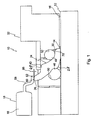
- FIG. 1 illustrates a test socket 10 in accordance with the present invention.
- the test socket 10 is intended for use with a tester typically employed for ascertaining quality of integrated circuit devices used in electronic appliances.
- the tester interfaces with a tester load board 12 which has electrically conductive traces 14 formed on a surface 16 thereof to enable electronic communication between the tester and an integrated circuit device 18 to be tested. That is, electrical signals are transmitted between the device under test 18 and the test apparatus through the test socket 10.
- FIG. 1 illustrates a leaded device having externally-extending leads 58 diverging from the body 59 of the device 18. It will be understood, however, that leadless devices, as illustrated in FIG. 2 , can be accommodated. Such devices have pads 61 rather than leads 58.
- FIG. 1 illustrates a device under test (DUT) package in an elevational view showing a single lead
- a plurality of leads 58 are typically part of the device 18.
- a contact 24, as will be discussed hereinafter, will be provided for engagement by each lead 58.
- substantially identical leads extend, in the case of the type of device 18 illustrated, along both of opposite sides of the device package 18.
- FIG. 1 illustrates a location of the device 18 and an orientation of contact 24 when lead 58 has first engaged the front, or inner, end 26 of contact 24.
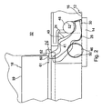
- FIG. 2 illustrates an orientation of contact 24 (a second orientation) when the device is in a test position. It will be understood that, in view of the construction of contact 24 as will be discussed hereinafter, an arcuate surface 28 at the rear end 30 of contact 24 will roll across trace 14 on the load board 12 with virtually no translational or rotational sliding of that surface along the trace 14.
- FIGS. 1 and 2 illustrate a wall 70 against which rear end 30 of contact 24 abuts. Such a wall 70 is defined in the housing of the test socket 10. It will be noted that the wall 70 is at a rather large acute angle with respect to the surface 16 of load board 12. Typically the angle is somewhere within a range of between 72°-78°. The wall 70 serves to be engaged by rear end 30 of contact 24 in order to preclude sliding of edge 28 along trace 14.
- the contact 24 illustrated in the drawing figures includes a protrusion 40.
- Protrusion 40 functions to engage, when mounted by elastomers 46 and 48, a shoulder 49 defined by the housing 32. Engagement of the shoulder 49 by protrusion 40 serves to limit the degree of upward movement of the contact 24 and the distance the front end 26 of the contact 24 will extend beyond an upper surface of the housing 32 when the contact 24 is not engaged by a device to be tested.
- elastomers 46, 48 affect mounting of contact 24.
- the test socket housing 32 is, therefore, provided with a pair of channels 50, 52 which extend along axes generally transverse to a plane defined by contact 24 when it is mounted in the housing 32.
- Elastomers 46, 48 are received within channels 50, 52 respectively.
- Rear elastomer 48 is pre-loaded and, as a result of the arcuate surface 28 at the rear end 30 of contact 24 being in engagement with the load board 12, will engage an upper edge of the rear end 30 of contact 24 at a location to urge the front end 26 of contact 24 upwardly.
- front elastomer 46 is under compression and also serves to urge contact 24 upward.
- Contact 24 will, in its neutral orientation, be positioned and oriented as seen in FIG. 1 . This is a first orientation of contact 24 and the one it occupies prior to a device 18 being brought into engagement with the upper end 26 of contact 24 by device 18.
- FIG. 1 illustrates multiple contact points defined by upper end 26 of contact 24.
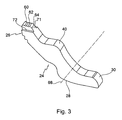
- the contact points are, as best seen in FIG. 3 , generally parallel extending ridges 60, 62, 64. While FIG. 3 illustrates three parallel ridges extending generally parallel to the axis 68, a smaller contact, as shown in FIGS. 1 and 2 , might well be provided with only two ridges 60, 62.
- FIG. 1 illustrates the locations of ridges 60, 62 relative to each other at the time of first engagement by lead 58 of device 18. It will be noted that ridge 60 is engaged by lead 58, and ridge 62 is not. The spacing between lead 58 and ridge 62, when the contact 24 is in this orientation, is illustrated by reference numeral 66.
- contact 24 will be caused to rotate generally counterclockwise about axis 68.
- lead 58 will engage ridge 62, and ridge 60 will be rotated downwardly away from lead 58.
- second ridge 62 will also be withdrawn from lead 58 as third ridge 64 engages the lead.
- the multiple ridge construction serves to help control a buildup of tin on front end 26 of contact 24.
- the first ridge 60 has a tendency to collect the most tin.
- a non-desirable buildup is deterred by providing multiple ridges.
- the first ridge serves a sacrificial function in absorbing the greatest transfer of tin.
- FIG. 3 illustrates a contact 24 having a narrowed front end 26.
- Such an embodiment defines a smaller land 71 with spaced shoulders 72 on either side thereof.
- Such a feature it is envisioned, would be used when the device being tested were leadless and had a pad generally flush with the bottom of the body of the device 18.
- Such a land embodiment could even serve to function in an environment wherein the pad or pads of the DUT are recessed within the body of the integrated circuit.
Landscapes
- Engineering & Computer Science (AREA)
- Computer Hardware Design (AREA)
- Microelectronics & Electronic Packaging (AREA)
- Physics & Mathematics (AREA)
- General Physics & Mathematics (AREA)
- Manufacturing & Machinery (AREA)
- Power Engineering (AREA)
- Testing Of Individual Semiconductor Devices (AREA)
- Measuring Leads Or Probes (AREA)
- Tests Of Electronic Circuits (AREA)
Priority Applications (1)
| Application Number | Priority Date | Filing Date | Title |
|---|---|---|---|
| EP12154283A EP2463666A3 (en) | 2006-02-24 | 2007-02-23 | Electronic device test set and contact used therein |
Applications Claiming Priority (2)
| Application Number | Priority Date | Filing Date | Title |
|---|---|---|---|
| US77665406P | 2006-02-24 | 2006-02-24 | |
| US11/677,870 US7639026B2 (en) | 2006-02-24 | 2007-02-22 | Electronic device test set and contact used therein |
Publications (3)
| Publication Number | Publication Date |
|---|---|
| EP1826575A2 EP1826575A2 (en) | 2007-08-29 |
| EP1826575A3 EP1826575A3 (en) | 2009-06-03 |
| EP1826575B1 true EP1826575B1 (en) | 2012-02-08 |
Family
ID=38110606
Family Applications (2)
| Application Number | Title | Priority Date | Filing Date |
|---|---|---|---|
| EP12154283A Withdrawn EP2463666A3 (en) | 2006-02-24 | 2007-02-23 | Electronic device test set and contact used therein |
| EP07003763A Active EP1826575B1 (en) | 2006-02-24 | 2007-02-23 | Electronic device test set and contact used therein |
Family Applications Before (1)
| Application Number | Title | Priority Date | Filing Date |
|---|---|---|---|
| EP12154283A Withdrawn EP2463666A3 (en) | 2006-02-24 | 2007-02-23 | Electronic device test set and contact used therein |
Country Status (8)
| Country | Link |
|---|---|
| US (1) | US7639026B2 (ja) |
| EP (2) | EP2463666A3 (ja) |
| JP (1) | JP5219383B2 (ja) |
| KR (1) | KR101522027B1 (ja) |
| CA (1) | CA2579697A1 (ja) |
| MY (1) | MY154288A (ja) |
| SG (1) | SG135138A1 (ja) |
| TW (1) | TWI429913B (ja) |
Families Citing this family (39)
| Publication number | Priority date | Publication date | Assignee | Title |
|---|---|---|---|---|
| JP2009043591A (ja) * | 2007-08-09 | 2009-02-26 | Yamaichi Electronics Co Ltd | Icソケット |
| US8278955B2 (en) | 2008-03-24 | 2012-10-02 | Interconnect Devices, Inc. | Test interconnect |
| US20090267629A1 (en) * | 2008-04-23 | 2009-10-29 | J. Foong Technologies Sdn. Bhd. | Contact for interconnect system in a test socket |
| US20090289647A1 (en) | 2008-05-01 | 2009-11-26 | Interconnect Devices, Inc. | Interconnect system |
| MY155348A (en) * | 2008-06-12 | 2015-10-15 | Multitest Elektronische Syst | Contact base |
| JP5029969B2 (ja) * | 2008-11-12 | 2012-09-19 | 山一電機株式会社 | 電気接続装置 |
| TW201027849A (en) | 2009-01-13 | 2010-07-16 | Yi-Zhi Yang | Connector |
| US8988090B2 (en) | 2009-04-21 | 2015-03-24 | Johnstech International Corporation | Electrically conductive kelvin contacts for microcircuit tester |
| US8558554B2 (en) * | 2009-04-21 | 2013-10-15 | Johnstech International Corporation | Electrically conductive Kelvin contacts for microcircuit tester |
| US9329204B2 (en) | 2009-04-21 | 2016-05-03 | Johnstech International Corporation | Electrically conductive Kelvin contacts for microcircuit tester |
| US9069011B2 (en) * | 2009-09-11 | 2015-06-30 | Exelon Generation Company, Llc | Electrical terminal test point and methods of use |
| US9700889B2 (en) | 2009-11-23 | 2017-07-11 | Cyvek, Inc. | Methods and systems for manufacture of microarray assay systems, conducting microfluidic assays, and monitoring and scanning to obtain microfluidic assay results |
| US9759718B2 (en) | 2009-11-23 | 2017-09-12 | Cyvek, Inc. | PDMS membrane-confined nucleic acid and antibody/antigen-functionalized microlength tube capture elements, and systems employing them, and methods of their use |
| US9500645B2 (en) | 2009-11-23 | 2016-11-22 | Cyvek, Inc. | Micro-tube particles for microfluidic assays and methods of manufacture |
| US9651568B2 (en) | 2009-11-23 | 2017-05-16 | Cyvek, Inc. | Methods and systems for epi-fluorescent monitoring and scanning for microfluidic assays |
| US10065403B2 (en) | 2009-11-23 | 2018-09-04 | Cyvek, Inc. | Microfluidic assay assemblies and methods of manufacture |
| US9855735B2 (en) | 2009-11-23 | 2018-01-02 | Cyvek, Inc. | Portable microfluidic assay devices and methods of manufacture and use |
| JP5701894B2 (ja) | 2009-11-23 | 2015-04-15 | サイヴェク・インコーポレイテッド | アッセイを行う方法及び装置 |
| WO2011145916A1 (en) * | 2010-05-21 | 2011-11-24 | Jf Microtechnology Sdn. Bhd. | An electrical interconnect assembly and a test contact for an electrical interconnect assembly |
| USD668625S1 (en) * | 2010-07-22 | 2012-10-09 | Titan Semiconductor Tool, LLC | Integrated circuit socket connector |
| SG195107A1 (en) * | 2011-05-27 | 2013-12-30 | Jf Microtechnology Sdn Bhd | An electrical interconnect assembly |
| KR200455379Y1 (ko) * | 2011-06-13 | 2011-09-01 | 나경화 | 반도체 칩 테스트용 핀 및 그를 포함한 반도체 칩 테스트용 소켓 |
| EP2822688B1 (en) | 2012-03-08 | 2019-09-25 | Cyvek, Inc. | Microfluidic assay assemblies and methods of manufacture |
| US9274141B1 (en) * | 2013-01-22 | 2016-03-01 | Johnstech International Corporation | Low resistance low wear test pin for test contactor |
| US10794933B1 (en) | 2013-03-15 | 2020-10-06 | Johnstech International Corporation | Integrated circuit contact test apparatus with and method of construction |
| EP2985614A4 (en) * | 2013-04-11 | 2016-12-21 | Renesas Electronics Corp | METHOD OF MANUFACTURING A SEMICONDUCTOR COMPONENT |
| TWI500222B (zh) * | 2013-07-12 | 2015-09-11 | Ccp Contact Probes Co Ltd | 連接器組合 |
| US10114039B1 (en) * | 2015-04-24 | 2018-10-30 | Johnstech International Corporation | Selectively geometric shaped contact pin for electronic component testing and method of fabrication |
| US9343830B1 (en) * | 2015-06-08 | 2016-05-17 | Xcerra Corporation | Integrated circuit chip tester with embedded micro link |
| US10436819B1 (en) | 2015-07-07 | 2019-10-08 | Johnstech International Corporation | Constant pressure pin tip for testing integrated circuit chips |
| US9958499B1 (en) | 2015-07-07 | 2018-05-01 | Johnstech International Corporation | Constant stress pin tip for testing integrated circuit chips |
| US10228367B2 (en) | 2015-12-01 | 2019-03-12 | ProteinSimple | Segmented multi-use automated assay cartridge |
| JP2018091643A (ja) * | 2016-11-30 | 2018-06-14 | 矢崎総業株式会社 | 磁界検出センサ |
| US11002760B1 (en) | 2017-02-06 | 2021-05-11 | Johnstech International Corporation | High isolation housing for testing integrated circuits |
| MX2020007325A (es) | 2017-09-25 | 2021-01-29 | Johnstech Int Corporation | Contactor de alto grado de aislamiento con clavija de prueba y carcasa para probar circuitos integrados. |
| USD942290S1 (en) * | 2019-07-12 | 2022-02-01 | Johnstech International Corporation | Tip for integrated circuit test pin |
| US11906576B1 (en) | 2021-05-04 | 2024-02-20 | Johnstech International Corporation | Contact assembly array and testing system having contact assembly array |
| US11867752B1 (en) | 2021-05-13 | 2024-01-09 | Johnstech International Corporation | Contact assembly and kelvin testing system having contact assembly |
| JP2024064692A (ja) * | 2022-10-28 | 2024-05-14 | 株式会社日本マイクロニクス | コンタクトピンおよび電気的接続装置 |
Family Cites Families (18)
| Publication number | Priority date | Publication date | Assignee | Title |
|---|---|---|---|---|
| US4321122A (en) * | 1980-03-31 | 1982-03-23 | Eastman Kodak Company | Apparatus for forming electrical contact with an analysis slide |
| US5207584A (en) * | 1991-01-09 | 1993-05-04 | Johnson David A | Electrical interconnect contact system |
| US5634801A (en) * | 1991-01-09 | 1997-06-03 | Johnstech International Corporation | Electrical interconnect contact system |
| US5781022A (en) * | 1991-06-04 | 1998-07-14 | Micron Technology, Inc. | Substrate having self limiting contacts for establishing an electrical connection with a semiconductor die |
| US5594355A (en) * | 1994-07-19 | 1997-01-14 | Delta Design, Inc. | Electrical contactor apparatus for testing integrated circuit devices |
| JP3675989B2 (ja) * | 1995-11-17 | 2005-07-27 | 株式会社テセック | 電子部品用コネクタ |
| DE29704035U1 (de) * | 1997-03-06 | 1997-05-22 | Fladung Gmbh Manfred | Vorrichtung zur Aufnahme bzw. zum Verstauen eines Kabels |
| JP2000156268A (ja) * | 1998-11-18 | 2000-06-06 | Kasasaku Electronics:Kk | Icソケット及びicソケット用コンタクトピン |
| US6255585B1 (en) * | 1999-01-29 | 2001-07-03 | Advantest Corp. | Packaging and interconnection of contact structure |
| JP2000228262A (ja) * | 1999-02-08 | 2000-08-15 | Mitsubishi Electric Corp | テストソケットのピン及び溝形成方法 |
| JP2001004698A (ja) * | 1999-06-18 | 2001-01-12 | Mitsubishi Electric Corp | テスト用ソケット、及びその接触端子の製造方法、並びに電子機器あるいは半導体パッケージ |
| US6794890B1 (en) * | 1999-07-27 | 2004-09-21 | Mitsubishi Denki Kabushiki Kaisha | Test socket, method of manufacturing the test socket, test method using the test socket, and member to be tested |
| JP2002093541A (ja) * | 2000-09-19 | 2002-03-29 | Miyazaki Oki Electric Co Ltd | Icソケット |
| KR100351676B1 (ko) * | 2000-10-12 | 2002-09-05 | 주식회사 우영 | 콘택핀 및 이것을 구비한 집적회로 패키지 테스트용 소켓 |
| US6854981B2 (en) * | 2002-06-03 | 2005-02-15 | Johnstech International Corporation | Small pin connecters |
| US7059866B2 (en) * | 2003-04-23 | 2006-06-13 | Johnstech International Corporation | integrated circuit contact to test apparatus |
| SG129245A1 (en) * | 2003-04-29 | 2007-02-26 | Tan Yin Leong | Improved probe for integrated circuit test socket |
| US7445465B2 (en) * | 2005-07-08 | 2008-11-04 | Johnstech International Corporation | Test socket |
-
2007
- 2007-02-22 US US11/677,870 patent/US7639026B2/en active Active
- 2007-02-23 MY MYPI20070275A patent/MY154288A/en unknown
- 2007-02-23 EP EP12154283A patent/EP2463666A3/en not_active Withdrawn
- 2007-02-23 SG SG200701278-4A patent/SG135138A1/en unknown
- 2007-02-23 EP EP07003763A patent/EP1826575B1/en active Active
- 2007-02-26 TW TW096106539A patent/TWI429913B/zh active
- 2007-02-26 CA CA002579697A patent/CA2579697A1/en not_active Abandoned
- 2007-02-26 KR KR1020070019224A patent/KR101522027B1/ko active IP Right Grant
- 2007-02-26 JP JP2007045642A patent/JP5219383B2/ja active Active
Also Published As
| Publication number | Publication date |
|---|---|
| TW200741210A (en) | 2007-11-01 |
| EP2463666A3 (en) | 2012-08-29 |
| KR20070088404A (ko) | 2007-08-29 |
| US20070236236A1 (en) | 2007-10-11 |
| KR101522027B1 (ko) | 2015-05-20 |
| TWI429913B (zh) | 2014-03-11 |
| JP2007248460A (ja) | 2007-09-27 |
| US7639026B2 (en) | 2009-12-29 |
| EP1826575A2 (en) | 2007-08-29 |
| EP2463666A2 (en) | 2012-06-13 |
| JP5219383B2 (ja) | 2013-06-26 |
| SG135138A1 (en) | 2007-09-28 |
| EP1826575A3 (en) | 2009-06-03 |
| CA2579697A1 (en) | 2007-08-24 |
| MY154288A (en) | 2015-05-29 |
Similar Documents
| Publication | Publication Date | Title |
|---|---|---|
| EP1826575B1 (en) | Electronic device test set and contact used therein | |
| US7445465B2 (en) | Test socket | |
| US10551412B2 (en) | Low resistance low wear test pin for test contactor | |
| JP2007248460A5 (ja) | ||
| KR100734296B1 (ko) | 자체 클리닝 기능이 있는 검사장치용 소켓핀 및 이를포함하는 검사장치 | |
| CA2122508C (en) | Apparatus for interconnecting electrical contacts | |
| EP1113273A2 (en) | System for testing bare IC chips and a socket for such chips | |
| CN106841691B (zh) | 插脚和半导体封装件测试系统 | |
| WO1999032895A1 (en) | Apparatus and method for testing a device | |
| KR20090005978A (ko) | 소켓용 어댑터 장치 | |
| TW201928362A (zh) | 檢查輔助具 | |
| US20080054924A1 (en) | Contact for interconnect system | |
| US4112363A (en) | Multicontact test probe apparatus | |
| US20090267629A1 (en) | Contact for interconnect system in a test socket | |
| US6572388B2 (en) | Socket for testing IC package | |
| KR100861568B1 (ko) | 클립과 프로브를 이용한 독립 모듈 소켓 | |
| JP4213455B2 (ja) | 電気部品用ソケット | |
| KR200372568Y1 (ko) | Fpc 검사용 지그 | |
| KR101041219B1 (ko) | 검사용 컨택모듈 | |
| US7077665B2 (en) | Contact pin and socket for electrical parts | |
| KR102188174B1 (ko) | 프로브핀에 의해 디스플레이 패널을 검사하는 소켓장치 | |
| EP3696555B1 (en) | Probe device of floating structure | |
| JPH11149953A (ja) | 電子機器 | |
| KR20050036108A (ko) | 모듈형 ic 소켓 | |
| EP4222509A1 (en) | Housing with anti-dislodge capability |
Legal Events
| Date | Code | Title | Description |
|---|---|---|---|
| PUAI | Public reference made under article 153(3) epc to a published international application that has entered the european phase |
Free format text: ORIGINAL CODE: 0009012 |
|
| AK | Designated contracting states |
Kind code of ref document: A2 Designated state(s): AT BE BG CH CY CZ DE DK EE ES FI FR GB GR HU IE IS IT LI LT LU LV MC NL PL PT RO SE SI SK TR |
|
| AX | Request for extension of the european patent |
Extension state: AL BA HR MK YU |
|
| RAP1 | Party data changed (applicant data changed or rights of an application transferred) |
Owner name: JOHNSTECH INTERNATIONAL CORPORATION |
|
| RIN1 | Information on inventor provided before grant (corrected) |
Inventor name: GILK,MATHEW L. Inventor name: SHELL, DENNIS B. Inventor name: LOPEZ, JOSE E. |
|
| PUAL | Search report despatched |
Free format text: ORIGINAL CODE: 0009013 |
|
| RIN1 | Information on inventor provided before grant (corrected) |
Inventor name: GILK,MATHEW L. Inventor name: SHELL, DENNIS B. Inventor name: LOPEZ, JOSE E. |
|
| AK | Designated contracting states |
Kind code of ref document: A3 Designated state(s): AT BE BG CH CY CZ DE DK EE ES FI FR GB GR HU IE IS IT LI LT LU LV MC NL PL PT RO SE SI SK TR |
|
| AX | Request for extension of the european patent |
Extension state: AL BA HR MK RS |
|
| RIN1 | Information on inventor provided before grant (corrected) |
Inventor name: GILK,MATHEW L. Inventor name: SHELL, DENNIS B. Inventor name: LOPEZ, JOSE E. |
|
| 17P | Request for examination filed |
Effective date: 20091203 |
|
| AKX | Designation fees paid |
Designated state(s): DE FR GB IE IT |
|
| 17Q | First examination report despatched |
Effective date: 20100205 |
|
| GRAP | Despatch of communication of intention to grant a patent |
Free format text: ORIGINAL CODE: EPIDOSNIGR1 |
|
| GRAS | Grant fee paid |
Free format text: ORIGINAL CODE: EPIDOSNIGR3 |
|
| GRAA | (expected) grant |
Free format text: ORIGINAL CODE: 0009210 |
|
| AK | Designated contracting states |
Kind code of ref document: B1 Designated state(s): DE FR GB IE IT |
|
| REG | Reference to a national code |
Ref country code: GB Ref legal event code: FG4D |
|
| REG | Reference to a national code |
Ref country code: DE Ref legal event code: R096 Ref document number: 602007020544 Country of ref document: DE Effective date: 20120405 |
|
| PLBE | No opposition filed within time limit |
Free format text: ORIGINAL CODE: 0009261 |
|
| STAA | Information on the status of an ep patent application or granted ep patent |
Free format text: STATUS: NO OPPOSITION FILED WITHIN TIME LIMIT |
|
| 26N | No opposition filed |
Effective date: 20121109 |
|
| REG | Reference to a national code |
Ref country code: DE Ref legal event code: R097 Ref document number: 602007020544 Country of ref document: DE Effective date: 20121109 |
|
| PGFP | Annual fee paid to national office [announced via postgrant information from national office to epo] |
Ref country code: IE Payment date: 20130215 Year of fee payment: 7 |
|
| REG | Reference to a national code |
Ref country code: IE Ref legal event code: MM4A |
|
| PG25 | Lapsed in a contracting state [announced via postgrant information from national office to epo] |
Ref country code: IE Free format text: LAPSE BECAUSE OF NON-PAYMENT OF DUE FEES Effective date: 20140223 |
|
| REG | Reference to a national code |
Ref country code: FR Ref legal event code: PLFP Year of fee payment: 10 |
|
| REG | Reference to a national code |
Ref country code: FR Ref legal event code: PLFP Year of fee payment: 11 |
|
| REG | Reference to a national code |
Ref country code: FR Ref legal event code: PLFP Year of fee payment: 12 |
|
| PGFP | Annual fee paid to national office [announced via postgrant information from national office to epo] |
Ref country code: FR Payment date: 20230220 Year of fee payment: 17 |
|
| PGFP | Annual fee paid to national office [announced via postgrant information from national office to epo] |
Ref country code: IT Payment date: 20230223 Year of fee payment: 17 |
|
| PGFP | Annual fee paid to national office [announced via postgrant information from national office to epo] |
Ref country code: DE Payment date: 20240219 Year of fee payment: 18 Ref country code: GB Payment date: 20240219 Year of fee payment: 18 |