EP1798780A2 - Verfahren zur Herstellung eines Substrats mit Nanostrukturen, lichtemittierende Vorrichtung und Verfahren zu deren Herstellung - Google Patents
Verfahren zur Herstellung eines Substrats mit Nanostrukturen, lichtemittierende Vorrichtung und Verfahren zu deren Herstellung Download PDFInfo
- Publication number
- EP1798780A2 EP1798780A2 EP06291934A EP06291934A EP1798780A2 EP 1798780 A2 EP1798780 A2 EP 1798780A2 EP 06291934 A EP06291934 A EP 06291934A EP 06291934 A EP06291934 A EP 06291934A EP 1798780 A2 EP1798780 A2 EP 1798780A2
- Authority
- EP
- European Patent Office
- Prior art keywords
- nano
- substrate
- light emitting
- protective film
- semiconductor layer
- Prior art date
- Legal status (The legal status is an assumption and is not a legal conclusion. Google has not performed a legal analysis and makes no representation as to the accuracy of the status listed.)
- Granted
Links
Images




Classifications
-
- H—ELECTRICITY
- H10—SEMICONDUCTOR DEVICES; ELECTRIC SOLID-STATE DEVICES NOT OTHERWISE PROVIDED FOR
- H10H—INORGANIC LIGHT-EMITTING SEMICONDUCTOR DEVICES HAVING POTENTIAL BARRIERS
- H10H20/00—Individual inorganic light-emitting semiconductor devices having potential barriers, e.g. light-emitting diodes [LED]
- H10H20/01—Manufacture or treatment
- H10H20/011—Manufacture or treatment of bodies, e.g. forming semiconductor layers
- H10H20/018—Bonding of wafers
-
- H—ELECTRICITY
- H10—SEMICONDUCTOR DEVICES; ELECTRIC SOLID-STATE DEVICES NOT OTHERWISE PROVIDED FOR
- H10H—INORGANIC LIGHT-EMITTING SEMICONDUCTOR DEVICES HAVING POTENTIAL BARRIERS
- H10H20/00—Individual inorganic light-emitting semiconductor devices having potential barriers, e.g. light-emitting diodes [LED]
- H10H20/01—Manufacture or treatment
- H10H20/011—Manufacture or treatment of bodies, e.g. forming semiconductor layers
- H10H20/013—Manufacture or treatment of bodies, e.g. forming semiconductor layers having light-emitting regions comprising only Group III-V materials
- H10H20/0133—Manufacture or treatment of bodies, e.g. forming semiconductor layers having light-emitting regions comprising only Group III-V materials with a substrate not being Group III-V materials
- H10H20/01335—Manufacture or treatment of bodies, e.g. forming semiconductor layers having light-emitting regions comprising only Group III-V materials with a substrate not being Group III-V materials the light-emitting regions comprising nitride materials
-
- H—ELECTRICITY
- H10—SEMICONDUCTOR DEVICES; ELECTRIC SOLID-STATE DEVICES NOT OTHERWISE PROVIDED FOR
- H10H—INORGANIC LIGHT-EMITTING SEMICONDUCTOR DEVICES HAVING POTENTIAL BARRIERS
- H10H20/00—Individual inorganic light-emitting semiconductor devices having potential barriers, e.g. light-emitting diodes [LED]
- H10H20/80—Constructional details
- H10H20/81—Bodies
- H10H20/819—Bodies characterised by their shape, e.g. curved or truncated substrates
- H10H20/82—Roughened surfaces, e.g. at the interface between epitaxial layers
Definitions
- the present invention relates to a method for fabricating a substrate with nano structures, a light emitting device and a manufacturing method thereof.
- a typical Light Emitting Diode is a single wave light source applied to various products, such as, but not limited thereto, backlights, signal lights, general illumination purposes and full color displays.
- Gallium nitride (GaN)-based and ZnO-based materials have a wide energy band gap of direct transition type, and many researches and developments thereto are being performed and commercialized recently as light sources of ultraviolet (UV), blue and green wavelength ranges.
- UV ultraviolet
- TIR total internal reflection
- the conventionally-structured LED suffers from a drawback of degraded light extraction efficiency, and many attempts have been made to improve this drawback.
- LED chips are ground into hemispherical shapes.
- a light emitting surface of the light emitting device is shaped into a hemisphere with an emitting layer at the center.
- Light emitted from a point in the active region of a hemispherically shaped light emitting device intersects the hemispherical interface at near normal incidence.
- total internal reflection is reduced.
- this technique although it is one of the best optical choices, is tedious and wasteful of material.
- defects introduced during the grinding process may compromise the reliability and performance of the light emitting devices.
- light emitting devices are encapsulated (encased) in a material with a dome or hemispherically shaped surface, although it is very difficult to manufacture.
- a light emitting device having a micro cavity structure or a resonant cavity structure is disclosed.
- this approach requires a very precise controllability and reproducibility relative to thickness of the structural layers during the fabrication process, and if the light is to be effectively extracted from semiconductors to air, this approach has a shortcoming in that the emitting wavelengths of the light emitting device should accurately match the fabricated cavity mode.
- Another shortcoming is that the emitting wavelengths of the light emitting device vary to drastically reduce the light extraction if temperatures or operating currents increase.
- the surface texturing technique is to roughen a surface of a light emitting device chip from which light generated thereinside is artificially emitted or to include a periodic pattern of the emitting surface.
- the surface texturing technique is actually applied in manufacturing the LEDs.
- a still another approach developed and applied for actual use is that patterns such as stripes, circles and lens are formed on a growth surface of a growth substrate like a sapphire before growing a light emitting structure for LEDs, and growth is performed of the LED structure, to minimize lattice defects of the grown light emitting structure and to enhance the quality, by which the light extraction efficiency of the LEDs can be improved.
- the approaches of the surface roughness and patterned substrate techniques known to enhance the light extracting efficiency from the light emitting device chip may be used individually, or applied in association with the known techniques such as the chip shape-changed technique and the epoxy encapsulation to improve the light extraction efficiency to a great extent.
- the surface texturing and patterned substrate techniques are typically embodied by photolithography in which a photoresist (PR) pattern is formed on an insulating layer by exposure using a mask and development, dry etching or wet etching process.
- PR photoresist
- LED light emitting device
- a method of fabricating a substrate with nano structures comprises: forming a protective film on the substrate and forming a thin film layer including a metal on the protective film; performing a thermal treatment process on the thin film including the metal and forming a plurality of nano agglomerations on the protective film; etching the protective film by using the plurality of agglomerations as a mask; removing the plurality of agglomerations and forming a plurality of nano structures on the substrate by etching a top surface of the substrate using the etched protective film as a mask; and removing the protective film.
- a method of fabricating a light emitting device comprises: forming a plurality of nano structures on a substrate; forming on the plurality of nano structures a light emitting structure comprised of a first semiconductor layer having a first polarity, an active layer and a second semiconductor layer having a polarity that is opposite to that of the first semiconductor; forming a support on the light emitting structure; removing the substrate from the light emitting structure; and removing the support, forming a first electrode on a bottom surface of the first semiconductor of the light emitting structure and forming a second electrode on the second semiconductor.
- a light emitting device comprises: a first semiconductor layer formed at a bottom surface thereof with a plurality of nano structures and having a first polarity; an active layer formed on a top surface of the first semiconductor layer; a second semiconductor layer formed on a top surface of the active layer and having a polarity that is opposite to the first polarity; a first electrode formed on a bottom surface of the first semiconductor layer; and a second electrode formed on a top surface of the second semiconductor layer.
- FIG.2 is a schematic perspective view illustrating an exemplary embodiment of a substrate formed with nano structures manufactured according to the present invention, where a substrate (100) is formed at a top surface thereof with a plurality of nano rods (105), and where the plurality of nano rods (105) comprises nano structures.
- Size of each of the nano rods (105) is 10nm ⁇ 2000nm, and although nano rods are regularly depicted in FIG.2, the nano rods may be irregularly arranged.
- FIG.3 is a schematic perspective view illustrating another exemplary embodiment of a substrate formed with nano structures manufactured according to the present invention, where a substrate (100) is formed at a top surface thereof with a plurality of grooves (135), and where the plurality of grooves (135) are also nano structures.
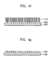
- FIGS.4a to 4g are cross-sectional views illustrating a fabricating method of a substrate formed with nano structures according to the present invention, where a substrate (100) is formed at a top surface thereof with a protective film (110) as shown in FIG.4a, and where the substrate (100) is preferred to be a sapphire substrate.
- the protective film (110) is SiO 2 or SiN which is a material easy for pattern forming by dry or wet etching, and easy for removal in a process that follow.
- thickness of the protective film (110) deposited on the substrate (100) is preferred to be 300nm.
- the protective film (110) is formed at a top surface thereof with a thin film layer (120) including a metal (FIG.4b).
- the thin film layer (120) including the metal may be not only the one including a very small quantity of metal but also the one including the metal only.
- the thin film layer (120) including the metal is formed with a metal having a thickness of several nm to several tens of nm by an E-Beam evaporation method.
- the protective film (110) not only blocks the thin film layer (120) including the evaporated metal from being diffused to or reacted with the substrate (100), but serves to control each size of agglomerations manufactured during a thermal process to a nano size.
- the thin film layer including the metal is successively thermally processed to allow forming a plurality of agglomerations (125), each of nano size, on the protective film (110).
- the thermal process of the thin film layer including the metal be implemented in the range of 100C ° to 2,000C ° by a Rapid Thermal Process equipment such as a Rapid Thermal Processing apparatus or a furnace.
- each size of the agglomerations (125) may be controlled by thickness of the thin film layer including the metal, temperature during the thermal process or thickness of the protective film.
- each width of the plurality of agglomerations (125) formed on the top surface of the protective film (110) be controlled within the range of 10nm to 2,000nm.
- the plurality of agglomerations (125) may be irregularly formed on the protective film (110), i.e., agglomerated in one lump or in several lumps, each being attached. Therefore, each size and discrete distance therebetween need not be regularly formed with a predetermined numerical value.
- the protective film (110) is etched utilizing the plurality of agglomerations (125) as a mask (FIG.4d). It is preferred that the protective film (110) be etched by performing a Reactive Ion Etching (RIE) process. It is apparent that the protective film (110) may be etched by various other dry etching processes than the RIE etching process.
- RIE Reactive Ion Etching
- the etching process according to the manufacturing method thus described in that it is easy and a high yield can be obtained with less manufacturing cost, compared with those methods embodying nanometer unit size such as lithography technologies including the conventional photolithography, E-beam Lithography, laser hologram, Deep UV Stepper.
- the plurality of agglomerations (125) is then removed (FIG.4e).
- the plurality of agglomerations may be removed by dry or wet etching process.
- the top surface of the substrate (100) is etched utilizing the etched protective film (115) as a mask to form a plurality of nano rods (105) on the top surface of the substrate (100) (FIG.4f).
- each width of the plurality of nano rods (105) formed on the substrate (100) is controlled within the range of 10nm to 2,000nm as that of the agglomerations.
- the substrate (100) may be etched by RIE method or other dry etching methods.
- the depth of the substrate (100) be appropriately adjusted and etched not to affect the supporting force of the substrate.
- the protective film (115) is removed (FIG.4g), which caps off the manufacturing of a substrate formed with the plurality of nano rods which is one kind of nano structures.
- a structure of nano grooves (not nano rods), or a mixture of nano rods with nano grooves may be formed on the substrate.
- the agglomerations are so formed as to allow some portions thereof to be attached to other portions, there are formed spaces at portions of the agglomeration not attached, and the substrate exposed to the spaces may be etched to form a plurality of grooves thereon.
- growth of a light emitting device epilayer on a substrate formed with nano stuructures such as nano rods and nano grooves has an advantage in that a crystal defect can be reduced and a high quality light emitting device can be embodied having an improved inner quantum efficiency and reliability.
- refraction and reflection from a substrate can be enhanced to thereby increase the light extraction efficiency and light output.
- a substrate formed with nano structures may be manufactured in a reverse order from the above exemplary embodiment in which a thermal process is first performed to form nano agglomerations by way of forming a thin film layer including a metal, and the agglomerations thus formed are utilized as a mask.
- FIG.5 is an exemplary SEM (Scanning Electron Microscope) graph of a substrate formed with nano structures according to the present invention, where the substrate (100) is formed at a top surface thereof with nano rods (105), and where the substrate (100) is preferred to be a sapphire substrate.
- SEM Sccanning Electron Microscope
- FIG.6 is a cross-sectional view illustrating an embodiment of a light emitting device using a substrate formed with nano structures according to the present invention, in which a substrate formed with nano structures is employed to form a horizontal light emitting device with an electrode disposed at a top surface thereof.
- the light emitting device is a light emitting structure comprising: a substrate formed thereon with a plurality of nano structures; a first semiconductor layer formed on the substrate and having a first polarity; an active layer; and a second semiconductor layer having a polarity opposite to the first polarity, where the first polarity is preferably n-type.
- the light emitting structure comprises: an n-type semiconductor layer formed on the substrate and etched at an upper partial portion thereof at a predetermined depth; an active layer formed at a remaining portion except the etched upper partial portion of the n-type semiconductor; and a p-type semiconductor layer formed on the active layer, where the n-type and p-type semiconductors are preferably GaN (gallium nitride) semiconductor layers.
- the light emitting device comprises: a substrate (200) formed thereon with nano rods (205); an n-type GaN layer (210) formed on the substrate (200) and an upper part thereof being partially removed; an active layer (220) formed on an un-removed n-type GaN layer; a p-type GaN layer (230) formed on the active layer (220); a first electrode (240) formed on removed n-type GaN layer (210); and a second electrode (250) formed on the p-type GaN layer (230), where the n-type GaN layer (210) is formed thereunder with a plurality of nano rod-shaped grooves, each width of which is preferably in the range of 10nm ⁇ 2,000nm.
- FIGS.7a to 7e are cross-sectional views illustrating a method for fabricating a light emitting device according to the present invention, where a method for manufacturing a vertical light emitting device capable of forming nano structures on a light emitting structure using a substrate formed with nano structures will be described.
- the light emitting device is formed with nano structures on a top surface of a second semiconductor layer or a bottom surface of a first semiconductor layer of a light emitting structure comprising: a first semiconductor layer having a first polarity; an active layer; and a second semiconductor layer having a polarity opposite to the first polarity, thereby enabling to enhance light extraction efficiency.
- the plurality of nano structures are first formed on the substrate (300) (FIG.7a), where the nano structures are nano rods (305), and the plurality of nano structures are formed in the same methods as those described in FIGS.4a to 4g.
- the substrate (300) disposed with a plurality of nano structures is formed thereon with a light emitting device (370), comprising: a first semiconductor layer (310) having a first polarity, an active layer (320); and a second semiconductor layer (330) having a polarity opposite to the first polarity (FIG.7b).
- a support (340) is formed on the light emitting structure (370) (FIG.7c). The support (340) is so formed as to support the light emitting structure (370) when the substrate (300) is to be separated in a subsequent process.
- the substrate (300) is then separated from the light emitting structure (370) .
- the separation of the substrate (300) is performed by the conventional LLO (Laser Lift-Off) process.
- first electrode (350) is formed under the first semiconductor layer (310) of the light emitting structure (370), and a second electrode (360) is formed on the second semiconductor layer (360) (FIG.7e).
- the completion of the above processes caps the manufacturing of the vertical light emitting device, and the first semiconductor layer (310) is formed thereunder with nano structures to thereby enhance the light extraction efficiency and the light output.
- the vertical type light emitting device comprises: a first semiconductor layer (310) formed at a bottom surface thereof with a plurality of nano structures and having a first polarity; an active layer (320) formed on a top surface of the first semiconductor layer (310); a second semiconductor layer (330) formed on a top surface of the active layer (320) and having a polarity that is opposite to the first polarity; a first electrode (350) formed on a bottom surface of the first semiconductor layer (310); and a second electrode (360) formed on a top surface of the second semiconductor layer (330).
- the first electrode (350) may be formed at a part or at an entire area of a bottom surface of the first semiconductor layer (310), and likewise, the second electrode (360) may also be formed at a part or at an entire area of a top surface of the second semiconductor layer (330).
- These electrodes may be freely changed in designs thereof in order to further enhance the light characteristics of the light emitting devices.
- the electrodes enter into a basic role for supplying holes and electrons to the active layer, and an additional layer may be interposed between the first electrode (350) and the first semiconductor layer (310), or between the second electrode (360) and the second semiconductor layer (320) for enhancing the characteristics of the light emitting device.
- the second electrode may be composed of a reflection ohmic electrode and a metal layer, where the reflection ohmic electrode may be formed on the top surface of the second semiconductor layer (320).
- the reflection ohmic electrode is formed at an entire area of the top surface of the second semiconductor layer (320), light advancing toward the top surface of the second semiconductor layer (320) in the vertical light emitting device is reflected from the reflection ohmic electrode to be discharged to the bottom surface of the first semiconductor layer (310), such that most of the light generated from the active layer (320) is discharged to the bottom surface of the first semiconductor layer (310) .
- the structure may be embodied in such a manner that the second electrode (360) is composed of a reflection ohmic electrode and a metal layer, where the reflection ohmic electrode is formed on a top surface of the second semiconductor layer (320), and the metal layer is formed thereon with a support.
- the method for fabricating the vertical light emitting device thus configured comprises: forming a reflection ohmic electrode and a metal layer on a light emitting structure; forming a support on the metal layer; removing a substrate; and forming another electrode on a surface of the light emitting structure. Therefore, the vertical light emitting device that has gone through the fabricating processes remains with the support.
- a substrate for growing a light emitting device is formed with nano agglomerations, and the substrate is etched by using the agglomerations as a mask to allow nano structures to be formed on the substrate, thereby enabling to grow a crystal defect-reduced, reliability-improved, good quality light emitting structure, and the light emitting structure is formed with nano structures to enable to enhance the light extraction efficiency.
- LED light emitting device
- Another advantage is that agglomerations are formed using a simple thermal treatment process and a substrate is etched by using the agglomerations as a mask, thereby enabling to form nano structures on the substrate with ease and less cost.
Landscapes
- Led Devices (AREA)
- Drying Of Semiconductors (AREA)
- Electroluminescent Light Sources (AREA)
Applications Claiming Priority (1)
| Application Number | Priority Date | Filing Date | Title |
|---|---|---|---|
| KR1020050123861A KR20070063731A (ko) | 2005-12-15 | 2005-12-15 | 나노 패턴이 형성된 기판의 제조방법 및 그 기판을 이용한발광소자 |
Publications (3)
| Publication Number | Publication Date |
|---|---|
| EP1798780A2 true EP1798780A2 (de) | 2007-06-20 |
| EP1798780A3 EP1798780A3 (de) | 2014-06-25 |
| EP1798780B1 EP1798780B1 (de) | 2020-10-07 |
Family
ID=37896060
Family Applications (1)
| Application Number | Title | Priority Date | Filing Date |
|---|---|---|---|
| EP06291934.5A Active EP1798780B1 (de) | 2005-12-15 | 2006-12-14 | Verfahren zur Herstellung einer lichtemittierenden Vorrichtung |
Country Status (5)
| Country | Link |
|---|---|
| US (1) | US8796698B2 (de) |
| EP (1) | EP1798780B1 (de) |
| JP (1) | JP5054366B2 (de) |
| KR (1) | KR20070063731A (de) |
| CN (1) | CN1983657B (de) |
Cited By (4)
| Publication number | Priority date | Publication date | Assignee | Title |
|---|---|---|---|---|
| WO2009039812A1 (de) * | 2007-09-28 | 2009-04-02 | Osram Opto Semiconductors Gmbh | Optoelektronischer halbleiterkörper |
| GB2488587A (en) * | 2011-03-03 | 2012-09-05 | Seren Photonics Ltd | Growth of iii-nitride layers for optoelectronic devices using a self-assembled nano-scale mask |
| EP2104754B1 (de) * | 2007-01-19 | 2019-07-03 | Nanogan Limited | Herstellung eines einzelkristallhalbleitermaterials mithilfe einer nanostrukturvorlage |
| WO2023148106A1 (de) * | 2022-02-01 | 2023-08-10 | Ams-Osram International Gmbh | Verfahren zur herstellung einer halbleiteranordnung und halbleiteranordnung |
Families Citing this family (43)
| Publication number | Priority date | Publication date | Assignee | Title |
|---|---|---|---|---|
| KR100654533B1 (ko) * | 2005-05-24 | 2006-12-06 | 엘지전자 주식회사 | 광 추출용 나노 로드를 갖는 발광 소자 및 그의 제조방법 |
| KR100965744B1 (ko) * | 2006-09-28 | 2010-06-24 | 주식회사 엘지화학 | 건식에칭에 의해 요철면이 형성된 기재의 제조방법, 상기방법으로 제조된 기재, 및 상기 기재를 포함하는 광전자소자 |
| KR100871649B1 (ko) * | 2007-06-26 | 2008-12-03 | 고려대학교 산학협력단 | 발광 다이오드의 사파이어 기판 패터닝 방법 |
| KR100955319B1 (ko) * | 2008-05-23 | 2010-04-29 | 고려대학교 산학협력단 | 발광다이오드 제조방법 및 이에 의해 제조되는발광다이오드 |
| KR101507127B1 (ko) * | 2008-06-30 | 2015-04-01 | 서울바이오시스 주식회사 | 패턴된 기판 및 질화물 반도체층 제조방법 |
| KR100956499B1 (ko) * | 2008-08-01 | 2010-05-07 | 주식회사 실트론 | 금속층을 가지는 화합물 반도체 기판, 그 제조 방법 및이를 이용한 화합물 반도체 소자 |
| EP2351097A2 (de) | 2008-10-23 | 2011-08-03 | Alta Devices, Inc. | Pv-element |
| KR101042333B1 (ko) * | 2008-12-01 | 2011-06-17 | 포항공과대학교 산학협력단 | 광원용 구조물의 제조방법과 이를 이용한 광원의 제조방법 |
| KR100994643B1 (ko) * | 2009-01-21 | 2010-11-15 | 주식회사 실트론 | 구형 볼을 이용한 화합물 반도체 기판의 제조 방법과 이를 이용한 화합물 반도체 기판 및 화합물 반도체 소자 |
| TWI469382B (zh) | 2009-03-30 | 2015-01-11 | 財團法人工業技術研究院 | 發光二極體結構與元件以及其製造方法 |
| TWI387003B (zh) * | 2009-04-24 | 2013-02-21 | 首爾大學校 產學協力團 | 形成有圖案之基板的製造方法 |
| TWI387004B (zh) * | 2009-04-24 | 2013-02-21 | 首爾大學校 產學協力團 | 形成有圖案之基板的製造方法 |
| WO2010123165A1 (en) * | 2009-04-24 | 2010-10-28 | Snu R&Db Foundation | Method of fabricating substrate where patterns are formed |
| CN102422444B (zh) * | 2009-04-29 | 2014-11-26 | 财团法人首尔大学校产学协力团 | 形成有图案的基板的制造方法 |
| KR101148444B1 (ko) * | 2009-06-19 | 2012-05-21 | 순천대학교 산학협력단 | 백색 나노 발광다이오드 및 이의 제조 방법 |
| KR101023135B1 (ko) * | 2009-07-13 | 2011-03-18 | 한국광기술원 | 이중요철구조의 기판을 갖는 반도체 발광소자 및 그 제조방법 |
| US9691921B2 (en) | 2009-10-14 | 2017-06-27 | Alta Devices, Inc. | Textured metallic back reflector |
| US9768329B1 (en) | 2009-10-23 | 2017-09-19 | Alta Devices, Inc. | Multi-junction optoelectronic device |
| US20150380576A1 (en) | 2010-10-13 | 2015-12-31 | Alta Devices, Inc. | Optoelectronic device with dielectric layer and method of manufacture |
| US9502594B2 (en) * | 2012-01-19 | 2016-11-22 | Alta Devices, Inc. | Thin-film semiconductor optoelectronic device with textured front and/or back surface prepared from template layer and etching |
| US20170141256A1 (en) | 2009-10-23 | 2017-05-18 | Alta Devices, Inc. | Multi-junction optoelectronic device with group iv semiconductor as a bottom junction |
| US9136422B1 (en) | 2012-01-19 | 2015-09-15 | Alta Devices, Inc. | Texturing a layer in an optoelectronic device for improved angle randomization of light |
| US11271128B2 (en) | 2009-10-23 | 2022-03-08 | Utica Leaseco, Llc | Multi-junction optoelectronic device |
| US8741417B2 (en) * | 2010-04-16 | 2014-06-03 | Korea University Research And Business Foundation | Films having switchable reflectivity |
| KR101215299B1 (ko) * | 2010-12-30 | 2012-12-26 | 포항공과대학교 산학협력단 | 나노 임프린트 몰드 제조방법, 이 방법에 의해 제조된 나노 임프린트 몰드를 이용한 발광다이오드 제조방법 및 이 방법에 의해 제조된 발광다이오드 |
| TWI459592B (zh) * | 2011-04-26 | 2014-11-01 | Univ Nat Chiao Tung | 奈米級側向成長磊晶之薄膜發光二極體及其製作方法 |
| CN102760802B (zh) * | 2011-04-29 | 2015-03-11 | 清华大学 | 发光二极管 |
| JP2012246216A (ja) * | 2011-05-25 | 2012-12-13 | Agency For Science Technology & Research | 基板上にナノ構造を形成させる方法及びその使用 |
| CN103782399B (zh) * | 2011-08-09 | 2016-11-09 | 三星电子株式会社 | 氮化物半导体发光元件 |
| KR101336100B1 (ko) * | 2011-10-06 | 2013-12-03 | 연세대학교 산학협력단 | 튜브형 단결정 실리콘 나노 구조물 및 그 제조방법 |
| CN103137797B (zh) * | 2011-12-03 | 2015-09-30 | 清华大学 | 发光二极管的制备方法 |
| CN103137796B (zh) * | 2011-12-03 | 2015-07-29 | 清华大学 | 发光二极管的制备方法 |
| CN103137798B (zh) * | 2011-12-03 | 2015-09-30 | 清华大学 | 发光二极管的制备方法 |
| KR20130072014A (ko) * | 2011-12-21 | 2013-07-01 | 엘지이노텍 주식회사 | 에피텍셜 기판 및 패턴 형성 방법 |
| US11038080B2 (en) | 2012-01-19 | 2021-06-15 | Utica Leaseco, Llc | Thin-film semiconductor optoelectronic device with textured front and/or back surface prepared from etching |
| KR101217783B1 (ko) * | 2012-04-24 | 2013-01-02 | 한국기계연구원 | 나노 패턴의 형성방법 |
| KR101417753B1 (ko) * | 2012-06-18 | 2014-07-14 | 제이엘씨(주) | 나노패턴을 갖는 플렉서블 기판 및 그 제조방법 |
| KR101323218B1 (ko) | 2012-07-26 | 2013-10-30 | 한국과학기술연구원 | 희생적 식각 마스크를 이용한 나노 구조물 제조방법 |
| CN102945900B (zh) * | 2012-12-11 | 2015-02-11 | 映瑞光电科技(上海)有限公司 | 一种纳米级图形化衬底的制造方法 |
| CN102983235B (zh) * | 2012-12-11 | 2015-04-01 | 映瑞光电科技(上海)有限公司 | 一种纳米级图形化衬底的制造方法 |
| KR101535236B1 (ko) * | 2013-05-06 | 2015-07-08 | 코닝정밀소재 주식회사 | 광추출 기판 및 이를 포함하는 유기발광소자 |
| KR101589348B1 (ko) * | 2013-08-01 | 2016-01-27 | 주식회사 엘지화학 | 나노 패턴 구조체의 제조방법 및 이를 이용한 반사 방지 필름의 제조방법과 제조장치 |
| CN114005912B (zh) * | 2021-10-29 | 2023-08-11 | 嘉兴学院 | 一种椭圆纳米棒、发光二极管的制备方法及显示装置 |
Family Cites Families (15)
| Publication number | Priority date | Publication date | Assignee | Title |
|---|---|---|---|---|
| JPH0992877A (ja) * | 1995-09-21 | 1997-04-04 | Shin Etsu Handotai Co Ltd | 半導体発光素子の製造方法 |
| US6518194B2 (en) | 2000-12-28 | 2003-02-11 | Thomas Andrew Winningham | Intermediate transfer layers for nanoscale pattern transfer and nanostructure formation |
| US6791119B2 (en) * | 2001-02-01 | 2004-09-14 | Cree, Inc. | Light emitting diodes including modifications for light extraction |
| JP4055503B2 (ja) * | 2001-07-24 | 2008-03-05 | 日亜化学工業株式会社 | 半導体発光素子 |
| CN1826286A (zh) | 2003-07-18 | 2006-08-30 | 日本电气株式会社 | 固定金属粒子的方法和采用这种固定方法制造含有金属粒子的衬底的方法、制造含有碳纳米管的衬底的方法及制造含有半导体 -晶体棒的衬底的方法 |
| JP2005064492A (ja) | 2003-07-28 | 2005-03-10 | Kyocera Corp | 単結晶サファイア基板とその製造方法及び半導体発光素子 |
| KR100714639B1 (ko) | 2003-10-21 | 2007-05-07 | 삼성전기주식회사 | 발광 소자 |
| JP4588638B2 (ja) * | 2003-11-04 | 2010-12-01 | パイオニア株式会社 | 半導体発光素子及びその製造方法 |
| TWI234298B (en) * | 2003-11-18 | 2005-06-11 | Itswell Co Ltd | Semiconductor light emitting diode and method for manufacturing the same |
| KR100576854B1 (ko) * | 2003-12-20 | 2006-05-10 | 삼성전기주식회사 | 질화물 반도체 제조 방법과 이를 이용한 질화물 반도체 |
| KR100634503B1 (ko) * | 2004-03-12 | 2006-10-16 | 삼성전자주식회사 | 질화물계 발광소자 및 그 제조방법 |
| US20050205883A1 (en) * | 2004-03-19 | 2005-09-22 | Wierer Jonathan J Jr | Photonic crystal light emitting device |
| US7161188B2 (en) * | 2004-06-28 | 2007-01-09 | Matsushita Electric Industrial Co., Ltd. | Semiconductor light emitting element, semiconductor light emitting device, and method for fabricating semiconductor light emitting element |
| KR20060131327A (ko) * | 2005-06-16 | 2006-12-20 | 엘지전자 주식회사 | 발광 다이오드의 제조 방법 |
| SG140473A1 (en) * | 2006-08-16 | 2008-03-28 | Tinggi Tech Private Ltd | Improvements in external light efficiency of light emitting diodes |
-
2005
- 2005-12-15 KR KR1020050123861A patent/KR20070063731A/ko not_active Ceased
-
2006
- 2006-12-14 EP EP06291934.5A patent/EP1798780B1/de active Active
- 2006-12-14 US US11/638,406 patent/US8796698B2/en active Active
- 2006-12-15 CN CN2006101700637A patent/CN1983657B/zh active Active
- 2006-12-15 JP JP2006338992A patent/JP5054366B2/ja not_active Expired - Fee Related
Cited By (7)
| Publication number | Priority date | Publication date | Assignee | Title |
|---|---|---|---|---|
| EP2104754B1 (de) * | 2007-01-19 | 2019-07-03 | Nanogan Limited | Herstellung eines einzelkristallhalbleitermaterials mithilfe einer nanostrukturvorlage |
| WO2009039812A1 (de) * | 2007-09-28 | 2009-04-02 | Osram Opto Semiconductors Gmbh | Optoelektronischer halbleiterkörper |
| US8362506B2 (en) | 2007-09-28 | 2013-01-29 | Osram Opto Semiconductors Gmbh | Optoelectronic semiconductor body |
| GB2488587A (en) * | 2011-03-03 | 2012-09-05 | Seren Photonics Ltd | Growth of iii-nitride layers for optoelectronic devices using a self-assembled nano-scale mask |
| US9034739B2 (en) | 2011-03-03 | 2015-05-19 | Seren Photonics Limited | Semiconductor devices and fabrication methods |
| GB2488587B (en) * | 2011-03-03 | 2015-07-29 | Seren Photonics Ltd | Semiconductor devices and fabrication methods |
| WO2023148106A1 (de) * | 2022-02-01 | 2023-08-10 | Ams-Osram International Gmbh | Verfahren zur herstellung einer halbleiteranordnung und halbleiteranordnung |
Also Published As
| Publication number | Publication date |
|---|---|
| US8796698B2 (en) | 2014-08-05 |
| CN1983657A (zh) | 2007-06-20 |
| KR20070063731A (ko) | 2007-06-20 |
| EP1798780B1 (de) | 2020-10-07 |
| JP5054366B2 (ja) | 2012-10-24 |
| EP1798780A3 (de) | 2014-06-25 |
| US20070166862A1 (en) | 2007-07-19 |
| CN1983657B (zh) | 2012-11-28 |
| JP2007168066A (ja) | 2007-07-05 |
Similar Documents
| Publication | Publication Date | Title |
|---|---|---|
| US8796698B2 (en) | Method for fabricating substrate with nano structures, light emitting device and manufacturing method thereof | |
| US7511308B2 (en) | Light emitting device and method for fabricating the same | |
| US8617909B2 (en) | LED with substrate modifications for enhanced light extraction and method of making same | |
| KR100654533B1 (ko) | 광 추출용 나노 로드를 갖는 발광 소자 및 그의 제조방법 | |
| JP4593890B2 (ja) | 半導体発光素子の製造方法 | |
| TWI385821B (zh) | 表面紋理化之發光二極體及其製造方法 | |
| US9461198B2 (en) | Backside transparent substrate roughening for UV light emitting diode | |
| JP2005317959A (ja) | 光結晶発光装置 | |
| CN102034907A (zh) | 一种提高GaN基LED发光效率的图形掩埋方法 | |
| CN208738290U (zh) | 一种图形化衬底、led外延片 | |
| JP2005064492A (ja) | 単結晶サファイア基板とその製造方法及び半導体発光素子 | |
| US7358537B2 (en) | Light emitting diode and fabrication method thereof | |
| CN108346718A (zh) | 利用低折射率材料为介质的复合图形衬底及其制作方法 | |
| KR100643473B1 (ko) | 나노 로드를 갖는 발광 소자 및 그의 제조 방법 | |
| KR100714626B1 (ko) | 질화물 반도체 발광소자 및 제조방법 | |
| KR101844871B1 (ko) | 광효율이 향상된 발광 다이오드 및 그 제조 방법 | |
| CN102751402B (zh) | 半导体发光元件和发光元件的制造方法 | |
| CN109920887B (zh) | 一种发光二极管芯片及其制造方法 | |
| KR100932500B1 (ko) | 광 추출 효율이 향상된 질화갈륨 소자 및 그 제작방법 | |
| CN115207175B (zh) | 基于图形化衬底的发光二极管芯片及其制备方法 | |
| KR102215920B1 (ko) | 발광소자용 기판 및 그 제조방법 | |
| KR102135530B1 (ko) | 발광소자용 기판 및 그 제조방법 | |
| CN115020563A (zh) | 一种具有微纳结构的图形衬底制备方法及外延结构 | |
| KR102135531B1 (ko) | 발광소자용 기판 및 그 제조방법 | |
| KR101335614B1 (ko) | 수직형 발광다이오드 소자 및 그 제조방법 |
Legal Events
| Date | Code | Title | Description |
|---|---|---|---|
| PUAI | Public reference made under article 153(3) epc to a published international application that has entered the european phase |
Free format text: ORIGINAL CODE: 0009012 |
|
| AK | Designated contracting states |
Kind code of ref document: A2 Designated state(s): AT BE BG CH CY CZ DE DK EE ES FI FR GB GR HU IE IS IT LI LT LU LV MC NL PL PT RO SE SI SK TR |
|
| AX | Request for extension of the european patent |
Extension state: AL BA HR MK YU |
|
| RAP1 | Party data changed (applicant data changed or rights of an application transferred) |
Owner name: LG INNOTEK CO., LTD. Owner name: LG ELECTRONICS, INC. |
|
| RIC1 | Information provided on ipc code assigned before grant |
Ipc: H01L 21/033 20060101ALI20140221BHEP Ipc: H01L 33/22 20100101ALN20140221BHEP Ipc: H01L 33/00 20100101AFI20140221BHEP Ipc: H01L 21/308 20060101ALI20140221BHEP |
|
| PUAL | Search report despatched |
Free format text: ORIGINAL CODE: 0009013 |
|
| RAP1 | Party data changed (applicant data changed or rights of an application transferred) |
Owner name: LG ELECTRONICS, INC. Owner name: LG INNOTEK CO., LTD. |
|
| AK | Designated contracting states |
Kind code of ref document: A3 Designated state(s): AT BE BG CH CY CZ DE DK EE ES FI FR GB GR HU IE IS IT LI LT LU LV MC NL PL PT RO SE SI SK TR |
|
| AX | Request for extension of the european patent |
Extension state: AL BA HR MK RS |
|
| RIC1 | Information provided on ipc code assigned before grant |
Ipc: H01L 33/22 20100101ALN20140519BHEP Ipc: H01L 21/308 20060101ALI20140519BHEP Ipc: H01L 33/00 20100101AFI20140519BHEP Ipc: H01L 21/033 20060101ALI20140519BHEP |
|
| 17P | Request for examination filed |
Effective date: 20141222 |
|
| RBV | Designated contracting states (corrected) |
Designated state(s): AT BE BG CH CY CZ DE DK EE ES FI FR GB GR HU IE IS IT LI LT LU LV MC NL PL PT RO SE SI SK TR |
|
| AKX | Designation fees paid |
Designated state(s): AT BE BG CH CY CZ DE DK EE ES FI FR GB GR HU IE IS IT LI LT LU LV MC NL PL PT RO SE SI SK TR |
|
| AXX | Extension fees paid |
Extension state: HR Extension state: BA Extension state: RS Extension state: MK Extension state: AL |
|
| RAP1 | Party data changed (applicant data changed or rights of an application transferred) |
Owner name: LG INNOTEK CO., LTD. Owner name: LG ELECTRONICS, INC. |
|
| STAA | Information on the status of an ep patent application or granted ep patent |
Free format text: STATUS: EXAMINATION IS IN PROGRESS |
|
| 17Q | First examination report despatched |
Effective date: 20190408 |
|
| GRAP | Despatch of communication of intention to grant a patent |
Free format text: ORIGINAL CODE: EPIDOSNIGR1 |
|
| STAA | Information on the status of an ep patent application or granted ep patent |
Free format text: STATUS: GRANT OF PATENT IS INTENDED |
|
| RIC1 | Information provided on ipc code assigned before grant |
Ipc: H01L 33/22 20100101ALN20200527BHEP Ipc: H01L 33/00 20100101AFI20200527BHEP |
|
| INTG | Intention to grant announced |
Effective date: 20200625 |
|
| GRAS | Grant fee paid |
Free format text: ORIGINAL CODE: EPIDOSNIGR3 |
|
| GRAA | (expected) grant |
Free format text: ORIGINAL CODE: 0009210 |
|
| STAA | Information on the status of an ep patent application or granted ep patent |
Free format text: STATUS: THE PATENT HAS BEEN GRANTED |
|
| REG | Reference to a national code |
Ref country code: DE Ref legal event code: R081 Ref document number: 602006059719 Country of ref document: DE Owner name: LG INNOTEK CO., LTD., KR Free format text: FORMER OWNERS: LG ELECTRONICS INC., SEOUL, KR; LG INNOTEK CO., LTD., SEOUL/SOUL, KR Ref country code: DE Ref legal event code: R081 Ref document number: 602006059719 Country of ref document: DE Owner name: SUZHOU LEKIN SEMICONDUCTOR CO. LTD., TAICANG, CN Free format text: FORMER OWNERS: LG ELECTRONICS INC., SEOUL, KR; LG INNOTEK CO., LTD., SEOUL/SOUL, KR Ref country code: DE Ref legal event code: R081 Ref document number: 602006059719 Country of ref document: DE Owner name: LG ELECTRONICS INC., KR Free format text: FORMER OWNERS: LG ELECTRONICS INC., SEOUL, KR; LG INNOTEK CO., LTD., SEOUL/SOUL, KR |
|
| AK | Designated contracting states |
Kind code of ref document: B1 Designated state(s): AT BE BG CH CY CZ DE DK EE ES FI FR GB GR HU IE IS IT LI LT LU LV MC NL PL PT RO SE SI SK TR |
|
| RAP1 | Party data changed (applicant data changed or rights of an application transferred) |
Owner name: LG ELECTRONICS, INC. Owner name: LG INNOTEK CO., LTD. |
|
| REG | Reference to a national code |
Ref country code: GB Ref legal event code: FG4D |
|
| REG | Reference to a national code |
Ref country code: AT Ref legal event code: REF Ref document number: 1322087 Country of ref document: AT Kind code of ref document: T Effective date: 20201015 Ref country code: CH Ref legal event code: EP |
|
| REG | Reference to a national code |
Ref country code: IE Ref legal event code: FG4D |
|
| REG | Reference to a national code |
Ref country code: DE Ref legal event code: R096 Ref document number: 602006059719 Country of ref document: DE |
|
| REG | Reference to a national code |
Ref country code: NL Ref legal event code: MP Effective date: 20201007 |
|
| REG | Reference to a national code |
Ref country code: AT Ref legal event code: MK05 Ref document number: 1322087 Country of ref document: AT Kind code of ref document: T Effective date: 20201007 |
|
| PG25 | Lapsed in a contracting state [announced via postgrant information from national office to epo] |
Ref country code: PT Free format text: LAPSE BECAUSE OF FAILURE TO SUBMIT A TRANSLATION OF THE DESCRIPTION OR TO PAY THE FEE WITHIN THE PRESCRIBED TIME-LIMIT Effective date: 20210208 Ref country code: NL Free format text: LAPSE BECAUSE OF FAILURE TO SUBMIT A TRANSLATION OF THE DESCRIPTION OR TO PAY THE FEE WITHIN THE PRESCRIBED TIME-LIMIT Effective date: 20201007 Ref country code: FI Free format text: LAPSE BECAUSE OF FAILURE TO SUBMIT A TRANSLATION OF THE DESCRIPTION OR TO PAY THE FEE WITHIN THE PRESCRIBED TIME-LIMIT Effective date: 20201007 Ref country code: GR Free format text: LAPSE BECAUSE OF FAILURE TO SUBMIT A TRANSLATION OF THE DESCRIPTION OR TO PAY THE FEE WITHIN THE PRESCRIBED TIME-LIMIT Effective date: 20210108 |
|
| REG | Reference to a national code |
Ref country code: LT Ref legal event code: MG4D |
|
| PG25 | Lapsed in a contracting state [announced via postgrant information from national office to epo] |
Ref country code: BG Free format text: LAPSE BECAUSE OF FAILURE TO SUBMIT A TRANSLATION OF THE DESCRIPTION OR TO PAY THE FEE WITHIN THE PRESCRIBED TIME-LIMIT Effective date: 20210107 Ref country code: AT Free format text: LAPSE BECAUSE OF FAILURE TO SUBMIT A TRANSLATION OF THE DESCRIPTION OR TO PAY THE FEE WITHIN THE PRESCRIBED TIME-LIMIT Effective date: 20201007 Ref country code: IS Free format text: LAPSE BECAUSE OF FAILURE TO SUBMIT A TRANSLATION OF THE DESCRIPTION OR TO PAY THE FEE WITHIN THE PRESCRIBED TIME-LIMIT Effective date: 20210207 Ref country code: ES Free format text: LAPSE BECAUSE OF FAILURE TO SUBMIT A TRANSLATION OF THE DESCRIPTION OR TO PAY THE FEE WITHIN THE PRESCRIBED TIME-LIMIT Effective date: 20201007 Ref country code: SE Free format text: LAPSE BECAUSE OF FAILURE TO SUBMIT A TRANSLATION OF THE DESCRIPTION OR TO PAY THE FEE WITHIN THE PRESCRIBED TIME-LIMIT Effective date: 20201007 Ref country code: PL Free format text: LAPSE BECAUSE OF FAILURE TO SUBMIT A TRANSLATION OF THE DESCRIPTION OR TO PAY THE FEE WITHIN THE PRESCRIBED TIME-LIMIT Effective date: 20201007 Ref country code: LV Free format text: LAPSE BECAUSE OF FAILURE TO SUBMIT A TRANSLATION OF THE DESCRIPTION OR TO PAY THE FEE WITHIN THE PRESCRIBED TIME-LIMIT Effective date: 20201007 |
|
| REG | Reference to a national code |
Ref country code: DE Ref legal event code: R097 Ref document number: 602006059719 Country of ref document: DE |
|
| PG25 | Lapsed in a contracting state [announced via postgrant information from national office to epo] |
Ref country code: EE Free format text: LAPSE BECAUSE OF FAILURE TO SUBMIT A TRANSLATION OF THE DESCRIPTION OR TO PAY THE FEE WITHIN THE PRESCRIBED TIME-LIMIT Effective date: 20201007 Ref country code: CZ Free format text: LAPSE BECAUSE OF FAILURE TO SUBMIT A TRANSLATION OF THE DESCRIPTION OR TO PAY THE FEE WITHIN THE PRESCRIBED TIME-LIMIT Effective date: 20201007 Ref country code: SK Free format text: LAPSE BECAUSE OF FAILURE TO SUBMIT A TRANSLATION OF THE DESCRIPTION OR TO PAY THE FEE WITHIN THE PRESCRIBED TIME-LIMIT Effective date: 20201007 Ref country code: RO Free format text: LAPSE BECAUSE OF FAILURE TO SUBMIT A TRANSLATION OF THE DESCRIPTION OR TO PAY THE FEE WITHIN THE PRESCRIBED TIME-LIMIT Effective date: 20201007 Ref country code: LT Free format text: LAPSE BECAUSE OF FAILURE TO SUBMIT A TRANSLATION OF THE DESCRIPTION OR TO PAY THE FEE WITHIN THE PRESCRIBED TIME-LIMIT Effective date: 20201007 |
|
| REG | Reference to a national code |
Ref country code: CH Ref legal event code: PL |
|
| PLBE | No opposition filed within time limit |
Free format text: ORIGINAL CODE: 0009261 |
|
| STAA | Information on the status of an ep patent application or granted ep patent |
Free format text: STATUS: NO OPPOSITION FILED WITHIN TIME LIMIT |
|
| PG25 | Lapsed in a contracting state [announced via postgrant information from national office to epo] |
Ref country code: MC Free format text: LAPSE BECAUSE OF FAILURE TO SUBMIT A TRANSLATION OF THE DESCRIPTION OR TO PAY THE FEE WITHIN THE PRESCRIBED TIME-LIMIT Effective date: 20201007 Ref country code: DK Free format text: LAPSE BECAUSE OF FAILURE TO SUBMIT A TRANSLATION OF THE DESCRIPTION OR TO PAY THE FEE WITHIN THE PRESCRIBED TIME-LIMIT Effective date: 20201007 |
|
| REG | Reference to a national code |
Ref country code: BE Ref legal event code: MM Effective date: 20201231 |
|
| 26N | No opposition filed |
Effective date: 20210708 |
|
| GBPC | Gb: european patent ceased through non-payment of renewal fee |
Effective date: 20210107 |
|
| REG | Reference to a national code |
Ref country code: DE Ref legal event code: R081 Ref document number: 602006059719 Country of ref document: DE Owner name: LG INNOTEK CO., LTD., KR Free format text: FORMER OWNERS: LG ELECTRONICS INC., SEOUL, KR; LG INNOTEK CO., LTD., SEOUL/SOUL, KR Ref country code: DE Ref legal event code: R081 Ref document number: 602006059719 Country of ref document: DE Owner name: SUZHOU LEKIN SEMICONDUCTOR CO. LTD., TAICANG, CN Free format text: FORMER OWNERS: LG ELECTRONICS INC., SEOUL, KR; LG INNOTEK CO., LTD., SEOUL/SOUL, KR Ref country code: DE Ref legal event code: R081 Ref document number: 602006059719 Country of ref document: DE Owner name: LG ELECTRONICS INC., KR Free format text: FORMER OWNERS: LG ELECTRONICS INC., SEOUL, KR; LG INNOTEK CO., LTD., SEOUL/SOUL, KR |
|
| PG25 | Lapsed in a contracting state [announced via postgrant information from national office to epo] |
Ref country code: IT Free format text: LAPSE BECAUSE OF FAILURE TO SUBMIT A TRANSLATION OF THE DESCRIPTION OR TO PAY THE FEE WITHIN THE PRESCRIBED TIME-LIMIT Effective date: 20201007 Ref country code: IE Free format text: LAPSE BECAUSE OF NON-PAYMENT OF DUE FEES Effective date: 20201214 Ref country code: LU Free format text: LAPSE BECAUSE OF NON-PAYMENT OF DUE FEES Effective date: 20201214 Ref country code: FR Free format text: LAPSE BECAUSE OF NON-PAYMENT OF DUE FEES Effective date: 20201231 |
|
| PG25 | Lapsed in a contracting state [announced via postgrant information from national office to epo] |
Ref country code: CH Free format text: LAPSE BECAUSE OF NON-PAYMENT OF DUE FEES Effective date: 20201231 Ref country code: GB Free format text: LAPSE BECAUSE OF NON-PAYMENT OF DUE FEES Effective date: 20210107 Ref country code: SI Free format text: LAPSE BECAUSE OF FAILURE TO SUBMIT A TRANSLATION OF THE DESCRIPTION OR TO PAY THE FEE WITHIN THE PRESCRIBED TIME-LIMIT Effective date: 20201007 Ref country code: LI Free format text: LAPSE BECAUSE OF NON-PAYMENT OF DUE FEES Effective date: 20201231 |
|
| PG25 | Lapsed in a contracting state [announced via postgrant information from national office to epo] |
Ref country code: IS Free format text: LAPSE BECAUSE OF FAILURE TO SUBMIT A TRANSLATION OF THE DESCRIPTION OR TO PAY THE FEE WITHIN THE PRESCRIBED TIME-LIMIT Effective date: 20210207 Ref country code: TR Free format text: LAPSE BECAUSE OF FAILURE TO SUBMIT A TRANSLATION OF THE DESCRIPTION OR TO PAY THE FEE WITHIN THE PRESCRIBED TIME-LIMIT Effective date: 20201007 Ref country code: CY Free format text: LAPSE BECAUSE OF FAILURE TO SUBMIT A TRANSLATION OF THE DESCRIPTION OR TO PAY THE FEE WITHIN THE PRESCRIBED TIME-LIMIT Effective date: 20201007 |
|
| PG25 | Lapsed in a contracting state [announced via postgrant information from national office to epo] |
Ref country code: BE Free format text: LAPSE BECAUSE OF NON-PAYMENT OF DUE FEES Effective date: 20201231 |
|
| REG | Reference to a national code |
Ref country code: DE Ref legal event code: R081 Ref document number: 602006059719 Country of ref document: DE Owner name: LG INNOTEK CO., LTD., KR Free format text: FORMER OWNERS: LG ELECTRONICS INC., SEOUL, KR; SUZHOU LEKIN SEMICONDUCTOR CO. LTD., TAICANG, SUZHOU, CN Ref country code: DE Ref legal event code: R081 Ref document number: 602006059719 Country of ref document: DE Owner name: LG ELECTRONICS INC., KR Free format text: FORMER OWNERS: LG ELECTRONICS INC., SEOUL, KR; SUZHOU LEKIN SEMICONDUCTOR CO. LTD., TAICANG, SUZHOU, CN |
|
| REG | Reference to a national code |
Ref country code: DE Ref legal event code: R079 Ref document number: 602006059719 Country of ref document: DE Free format text: PREVIOUS MAIN CLASS: H01L0033000000 Ipc: H10H0020000000 |
|
| PGFP | Annual fee paid to national office [announced via postgrant information from national office to epo] |
Ref country code: DE Payment date: 20241121 Year of fee payment: 19 |