EP1796256B1 - Piezoelectric device and piezoelectric switch employing same - Google Patents
Piezoelectric device and piezoelectric switch employing same Download PDFInfo
- Publication number
- EP1796256B1 EP1796256B1 EP05757801A EP05757801A EP1796256B1 EP 1796256 B1 EP1796256 B1 EP 1796256B1 EP 05757801 A EP05757801 A EP 05757801A EP 05757801 A EP05757801 A EP 05757801A EP 1796256 B1 EP1796256 B1 EP 1796256B1
- Authority
- EP
- European Patent Office
- Prior art keywords
- piezoelectric
- piezoelectric element
- pair
- plate
- piezoelectric device
- Prior art date
- Legal status (The legal status is an assumption and is not a legal conclusion. Google has not performed a legal analysis and makes no representation as to the accuracy of the status listed.)
- Not-in-force
Links
- 239000000463 material Substances 0.000 claims description 22
- 230000005611 electricity Effects 0.000 claims description 18
- 239000012212 insulator Substances 0.000 claims description 4
- 230000010287 polarization Effects 0.000 abstract description 21
- 230000002040 relaxant effect Effects 0.000 abstract 1
- 229910052751 metal Inorganic materials 0.000 description 89
- 239000002184 metal Substances 0.000 description 89
- 230000006835 compression Effects 0.000 description 11
- 238000007906 compression Methods 0.000 description 11
- 230000000694 effects Effects 0.000 description 10
- 238000004519 manufacturing process Methods 0.000 description 6
- 239000000853 adhesive Substances 0.000 description 5
- 230000001070 adhesive effect Effects 0.000 description 5
- 229910052451 lead zirconate titanate Inorganic materials 0.000 description 5
- 230000000593 degrading effect Effects 0.000 description 4
- 238000000605 extraction Methods 0.000 description 4
- 229920005989 resin Polymers 0.000 description 4
- 239000011347 resin Substances 0.000 description 4
- 239000000919 ceramic Substances 0.000 description 3
- 238000006243 chemical reaction Methods 0.000 description 3
- 239000003822 epoxy resin Substances 0.000 description 3
- 238000000034 method Methods 0.000 description 3
- 229920000647 polyepoxide Polymers 0.000 description 3
- RYGMFSIKBFXOCR-UHFFFAOYSA-N Copper Chemical compound [Cu] RYGMFSIKBFXOCR-UHFFFAOYSA-N 0.000 description 2
- KDLHZDBZIXYQEI-UHFFFAOYSA-N Palladium Chemical compound [Pd] KDLHZDBZIXYQEI-UHFFFAOYSA-N 0.000 description 2
- 230000008602 contraction Effects 0.000 description 2
- 229910052802 copper Inorganic materials 0.000 description 2
- 239000010949 copper Substances 0.000 description 2
- 230000007423 decrease Effects 0.000 description 2
- 230000005684 electric field Effects 0.000 description 2
- HFGPZNIAWCZYJU-UHFFFAOYSA-N lead zirconate titanate Chemical compound [O-2].[O-2].[O-2].[O-2].[O-2].[Ti+4].[Zr+4].[Pb+2] HFGPZNIAWCZYJU-UHFFFAOYSA-N 0.000 description 2
- 230000002093 peripheral effect Effects 0.000 description 2
- 238000003825 pressing Methods 0.000 description 2
- 238000007639 printing Methods 0.000 description 2
- 229920001187 thermosetting polymer Polymers 0.000 description 2
- 229910000906 Bronze Inorganic materials 0.000 description 1
- 229920000049 Carbon (fiber) Polymers 0.000 description 1
- OAICVXFJPJFONN-UHFFFAOYSA-N Phosphorus Chemical compound [P] OAICVXFJPJFONN-UHFFFAOYSA-N 0.000 description 1
- BQCADISMDOOEFD-UHFFFAOYSA-N Silver Chemical compound [Ag] BQCADISMDOOEFD-UHFFFAOYSA-N 0.000 description 1
- RTAQQCXQSZGOHL-UHFFFAOYSA-N Titanium Chemical compound [Ti] RTAQQCXQSZGOHL-UHFFFAOYSA-N 0.000 description 1
- 238000005452 bending Methods 0.000 description 1
- 239000010974 bronze Substances 0.000 description 1
- 239000004917 carbon fiber Substances 0.000 description 1
- 239000004020 conductor Substances 0.000 description 1
- KUNSUQLRTQLHQQ-UHFFFAOYSA-N copper tin Chemical compound [Cu].[Sn] KUNSUQLRTQLHQQ-UHFFFAOYSA-N 0.000 description 1
- 239000013013 elastic material Substances 0.000 description 1
- 239000010408 film Substances 0.000 description 1
- 230000000977 initiatory effect Effects 0.000 description 1
- 238000010030 laminating Methods 0.000 description 1
- WABPQHHGFIMREM-UHFFFAOYSA-N lead(0) Chemical compound [Pb] WABPQHHGFIMREM-UHFFFAOYSA-N 0.000 description 1
- 229910052763 palladium Inorganic materials 0.000 description 1
- 238000007650 screen-printing Methods 0.000 description 1
- 229910052709 silver Inorganic materials 0.000 description 1
- 239000004332 silver Substances 0.000 description 1
- 238000004544 sputter deposition Methods 0.000 description 1
- 239000000758 substrate Substances 0.000 description 1
- 239000010409 thin film Substances 0.000 description 1
- 239000010936 titanium Substances 0.000 description 1
- 229910052719 titanium Inorganic materials 0.000 description 1
Images


Classifications
-
- H—ELECTRICITY
- H03—ELECTRONIC CIRCUITRY
- H03K—PULSE TECHNIQUE
- H03K17/00—Electronic switching or gating, i.e. not by contact-making and –breaking
- H03K17/94—Electronic switching or gating, i.e. not by contact-making and –breaking characterised by the way in which the control signals are generated
- H03K17/965—Switches controlled by moving an element forming part of the switch
-
- H—ELECTRICITY
- H03—ELECTRONIC CIRCUITRY
- H03K—PULSE TECHNIQUE
- H03K17/00—Electronic switching or gating, i.e. not by contact-making and –breaking
- H03K17/94—Electronic switching or gating, i.e. not by contact-making and –breaking characterised by the way in which the control signals are generated
- H03K17/96—Touch switches
- H03K17/964—Piezoelectric touch switches
-
- H—ELECTRICITY
- H10—SEMICONDUCTOR DEVICES; ELECTRIC SOLID-STATE DEVICES NOT OTHERWISE PROVIDED FOR
- H10N—ELECTRIC SOLID-STATE DEVICES NOT OTHERWISE PROVIDED FOR
- H10N30/00—Piezoelectric or electrostrictive devices
- H10N30/30—Piezoelectric or electrostrictive devices with mechanical input and electrical output, e.g. functioning as generators or sensors
- H10N30/304—Beam type
- H10N30/306—Cantilevers
Definitions
- the present invention relates to a piezoelectric device including a piezoelectric element to which an elastic conductive member is fixed, and to a piezoelectric switch provided with the same.
- an electric generator which excites a piezoelectric element and allows it to vibrate freely to generate electricity
- a switching circuit which includes such an electric generator
- the above electric generator causes a piezoelectric body to expand and contract by bending a metal plate to which a polarized piezoelectric body in a thin plate-like shape is joined, and generates a voltage using a piezoelectric lateral effect. Therefore, either surface of the plate-shaped piezoelectric element has to be restricted by the metal plate.
- a unimorph type in which a plate-shaped piezoelectric element provided with electrodes at both sides is fixed to one surface of a metal plate
- a bimorph type in which a similar piezoelectric element is fixed to both surfaces of a metal plate.
- a piezoelectric element and a metal plate are generally joined using a thermosetting resin in a heated state. Therefore, the metal plate often employs a material having the same level of low coefficient of thermal expansion as that of the piezoelectric element.
- a piezoelectric actuator has been known, which has the same structure as that of the above electric generator and utilizes an inverse piezoelectric effect.
- some actuators have a structure in which a piezoelectric body is formed on a substrate having a thermal expansion coefficient greater than that of the piezoelectric body to reduce tensile stress within the piezoelectric body (for example, refer to patent document 3) .
- the piezoelectric actuator preserves mechanical strength of thin film of the piezoelectric body to prevent the film from being cracked or broken due to the tensile stress.
- the surface of the piezoelectric element is easily cracked due to a tensile stress generated within the piezoelectric element in an expansion state thereof.
- the piezoelectric element is bent together with the metal plate due to an impact of external force or by an external force, if the piezoelectric element is located at a curvature center side of the bent metal plate, a compression stress is generated within the piezoelectric element; while if the piezoelectric element is located at an opposite side of the curvature center of the bent metal plate, a tensile stress is generated within the piezoelectric element.
- the electric generator is subjected to an uncontrollable external force, and therefore likely to suffer from a stress exceeding its tensile strength. Further, when the surface of the piezoelectric element suffers cracks and the electrode on the surface of the element is divided, the area of the element surface contributing to the generation of electricity is reduced to an extremely small level to fail in generating satisfactory electric power.
- the piezoelectric actuator disclosed in the patent document 3 since the piezoelectric body is formed on a metal plate having a large thermal expansion coefficient, durability against the tensile stress is improved. However, since a piece of plate-shaped piezoelectric body is joined to a piece of metal plate in a heated state, the contraction of the metal plate is larger than that of the piezoelectric body, which easily causes the piezoelectric actuator to warp.
- An object of the present invention is to provide a piezoelectric device, which is hardly warped, by reducing the tensile stress generated within the piezoelectric element due to an external force to prevent the surface of the piezoelectric element from being cracked, and to provide a piezoelectric switch utilizing the same.
- a piezoelectric device is defined in claim 1.
- a pair of elastic conductive members is fixed to both main surfaces of the piezoelectric element. Owing to this, the piezoelectric element is prevented from being extremely deformed due to an impact of an external force or by an external force, thus the surface of the piezoelectric element is prevented from being cracked due to a stress. Even when the surface of the piezoelectric element is cracked and the electrode on the surface of the element is divided, area of the element contributing to generation of electricity is preserved and satisfactory electric power can be obtained without degrading its properties. Moreover, two pieces of conductive members sandwich a piece of piezoelectric body having a plate-like shape, thereby preventing the piezoelectric element from being warped.
- an elastic modulus of the pair of conductive members is larger than that of the piezoelectric element. This enables the piezoelectric element to easily follow the movement of the conductive members.
- the piezoelectric element is held by the pair of conductive members fixed to both main surfaces thereof being compressed in a direction parallel to the main surfaces.
- the coefficient of thermal expansion of the pair of conductive members is larger than that of the piezoelectric element. Owing to this, the conductive members, which are cooled after being bonded to the piezoelectric element, contract and hold the piezoelectric element while compressing the same in a direction parallel to the both main surfaces.
- the material of the elastic conductive member fixed to one electrode of the piezoelectric element is the same as that of the elastic conductive member fixed to the other electrode. Owing to this, since the piezoelectric device has a symmetrical structure with respect to the piezoelectric element, the compression stress acts thereon uniformly, thus the warp can be further prevented. Moreover, when the piezoelectric element and the conductive members are in free vibration, quality factor Q becomes larger, thus the conversion efficiency of the energy can be increased.
- the piezoelectric element has a rectangular plate-like shape
- the pair of conductive members have a rectangular plate-like shape, longer in one longitudinal direction than the piezoelectric element and protrude in one longitudinal direction from the piezoelectric element
- a fixing portion for supporting and fixing a pair of end portions of the conductive members protruding in one longitudinal direction from the piezoelectric element is further provided
- the fixing portion is provided with an insulator between a pair of end portions of the conductive members protruding in one longitudinal direction from the piezoelectric element.
- the conductive members may be used as extraction electrodes as they are.
- the piezoelectric element has a rectangular plate-like shape, in which the piezoelectric body is longer in one longitudinal direction than the pair of electrodes, a fixing portion for supporting and fixing a pair of end portions of the conductive members fixed to the piezoelectric body is further provided.
- the energy loss can be reduced.
- the piezoelectric body is not polarized.
- the conductive members can be utilized as extraction electrodes as they are. Only by adjusting the area for the electrode to be printed, the piezoelectric device can be made easily, and thus the labor and cost can be reduced.
- a piezoelectric device according to a further aspect of the present invention is defined in claim 8.
- the piezoelectric device of the present invention is provided with elastic conductive members respectively at the outer side of the first piezoelectric element and the second piezoelectric element. Owing to this arrangement, since the piezoelectric elements are not extremely deformed due to an impact of external force or by an external force, the surfaces of the piezoelectric elements are prevented from being cracked due to the stress. Even when the surface of the piezoelectric elements is cracked and the electrode on the surface of the element is divided, the area of the element contributing to the generation of electricity is preserved, thus satisfactory electric power can be obtained without degrading its properties. Moreover, since the piezoelectric body having a plate-like shape is sandwiched by the conductive members, the piezoelectric elements are prevented from warping. Further, since two pieces of the piezoelectric elements are used, even when the piezoelectric elements are thin, a large voltage can be obtained.
- a piezoelectric switch of the present invention comprises the above piezoelectric devices, an external force transmitting section for transmitting an external force to bend the piezoelectric element and the conductive member of the piezoelectric device, and a signal generating circuit that takes out a voltage generated by the piezoelectric element vibrated by a transmitted external force from a pair of conductive members and converts the voltage into an electric signal.
- the piezoelectric element is not extremely deformed due to an impact of an external force or by an external force. Therefore, the surface of the piezoelectric element is prevented from being cracked causing a breakage of the piezoelectric switch. Even when the surface of the piezoelectric element gets a crack and the electrode is divided, the area of the element contributing to generation of the electricity can be preserved, and thus a satisfactory electric signal can be obtained as the switch. Moreover, by adopting a structure such that a piece of piezoelectric member having a plate-like shape is sandwiched by the two pieces of the conductive members, the piezoelectric element is prevented from warping, and thus the piezoelectric switch, which is easy to manufacture and hardly broken, can be achieved.
- the piezoelectric device according to the present invention is not extremely deformed due to an impact of an external force or by an external force. Therefore, the surface of the piezoelectric element is prevented from being cracked. Even when the surface of the piezoelectric element gets a crack and the electrode is divided, the area of the element contributing to the generation of electricity can be preserved, and thus a satisfactory electric power can be obtained. Moreover, by adopting a structure such that a piece of piezoelectric body having a plate-like shape is sandwiched by the two pieces of the conductive members, the piezoelectric element can be prevented from being warped.
- the piezoelectric element is not extremely deformed due to an impact of an external force or by an external force. Therefore, the surface of the piezoelectric element is prevented from being cracked and the piezoelectric switch is prevented from being broken. Even when the surface of the piezoelectric element gets a crack and the electrode is divided, the area of the element contributing to the generation of electricity can be preserved, and thus a satisfactory electric signal can be obtained as the switch.
- the piezoelectric element is prevented from warping, and thus the piezoelectric switch, which is easy to manufacture and hardly broken, can be achieved.
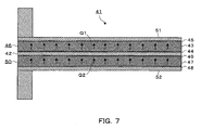
- Fig. 1 is a sectional view of a piezoelectric device 1.
- the piezoelectric device 1 comprises a piezoelectric element 4 including a piezoelectric body 2 and electrodes 3, metal plates 6 and fixing portions 10 as shown in Fig. 1 .
- the material of the piezoelectric body 2 is, for example, a lead zirconate titanate (PZT)-based piezoelectric ceramics.
- the material of the piezoelectric member is not particularly limited to a specific material, but any material other than PZT may be used as long as it is a piezoelectric body.
- the piezoelectric body 2 has a rectangular plate-like shape and is polarized in a direction indicated with arrows in Fig. 1 . However, the shape of the piezoelectric body 2 is not limited to a rectangular plate-like shape.
- the material of the electrodes 3 is a conductor such as silver, palladium or copper.
- the electrodes 3 are thinly printed on both main surfaces of the piezoelectric body 2.
- the plate-like piezoelectric element 4 is constructed of the piezoelectric body 2 and the electrodes 3.
- the term "main surfaces" mean widest surfaces in the surfaces of the plate-like body, which are opposite to each other in the thickness direction thereof.
- thermal splaying, sputtering or the like may be used as a method for thinly forming the electrodes on the both main surfaces of the piezoelectric body. Since the electrodes are thinly formed, the entire piezoelectric element receives little influence therefrom and the influence is negligible with respect to the elastic modulus or coefficient of thermal expansion. That is, the elastic modulus and the coefficient of thermal expansion of the piezoelectric element are substantially the same as those of the piezoelectric body.
- the piezoelectric element 4 has a pair of metal plates 6 fixed to the both main surfaces thereof as conductive members. Owing to this, even when the piezoelectric element 4 is bent together with the metal plate 6 by an impact of external force or due to an external force, the piezoelectric element 4 is prevented from being extremely skewed, and thus the surface of the piezoelectric element 4 can be prevented from being cracked due to a stress. Also, even when the piezoelectric element 4 suffers a crack on the surfaces thereof and the electrodes 3 are divided, the piezoelectric element 4 preserves the area contributing to the generation of electricity and provides satisfactory electric power without degrading its properties.
- the material of the metal plates 6 is preferably a material for spring having a larger elastic modulus and coefficient of thermal expansion than those of the piezoelectric element 4 like SUS, phosphor bronze, titanium, stainless or copper.
- the metal plates 6 and the piezoelectric element 4 are bonded to one another in a heated state and cooled to a room temperature, and are put into use. Being cooled, the metal plates 6 contract and hold the piezoelectric element 4 while compressing the same in a direction parallel to the both main surfaces.
- the metal plates 6 fixed to the both main surfaces give a compression stress to the piezoelectric element 4. That is, the metal plates 6 compress the piezoelectric element 4 in the direction parallel to the both main surfaces. As a result, a tensile stress caused from vibration of the piezoelectric element 4 can be reduced. Moreover, the piezoelectric element 4 is made to easily follow the movement of the metal plates 6.
- the material for the metal plate 6 in addition to the above materials, a material in which conductive ceramics is mixed with a conductive resin, or a conductive elastic material such as a resin including carbon fibers may be used. Both of the pair of metal plates 6 are formed in the same shape using preferably the same material. Owing to this, the piezoelectric device 1 has a symmetrical structure with respect to the piezoelectric element 4. Therefore, a uniform compression stress acts on the piezoelectric device 1, thus the piezoelectric device 1 can be further prevented from warping. Moreover, when the piezoelectric element 4 and the metal plates 6 are allowed to be in free vibration freely, the quality factor Q is further increased and the conversion efficiency of energy can be improved.
- the piezoelectric element 4 and the metal plates 6 are fixed to one another using an adhesive such as a thermosetting resin.
- the plate-like body is formed by laminating the pair of metal plates 6 so as to sandwich the piezoelectric element 4 as shown in the sectional view of Fig. 1 .
- the metal plates 6 are fixed to the piezoelectric element 4 so that the piezoelectric element 4 receives a compression stress in a direction parallel to the main surfaces at a room temperature. Owing to this, the compression stress is given to the piezoelectric element 4 in advance, thereby reducing the tensile stress, which is generated within the piezoelectric element by an external force. As a result, the surfaces of the piezoelectric element 4 can be prevented from being cracked by the tensile stress generated within the piezoelectric element 4.
- the piezoelectric element 4 when the piezoelectric element 4 receives a compression stress in a direction parallel to the main surfaces while the piezoelectric device 1 is in use, an effect to reduce the tensile stress is obtained. Therefore, when the piezoelectric device 1 is intended to be used at a room temperature or lower, the piezoelectric element 4 and the metal plates 6 may be fixed to one another at a room temperature using an adhesive which hardens at a room temperature. Also, the adhesive may be a conductive adhesive.
- the plate-like body is fixed by the fixing portions 10 at one end thereof, thus the piezoelectric device 1 has a structure of cantilever.
- the fixing portions 10 fix the plate-like body fixing at one end thereof by physically fastening the same from both main surfaces sides.
- An adhesive may be used for fixing the plate-like body.
- the lead zirconate titanate (PZT)-based piezoelectric body 2 is made using a common manufacturing method of piezoelectric ceramics. Electrodes are printed on the both main surfaces of the piezoelectric body 2 in a manner of screen printing, thus the piezoelectric element 4 having a plate-like shape is obtained. A pair of metal plates 6 is bonded onto the both main surfaces of the piezoelectric element 4 with an epoxy resin as shown in Fig. 2 ⁇ . And then, the piezoelectric element 4 and the metal plates 6 are heated while thermocompression bond.
- PZT lead zirconate titanate
- the piezoelectric element 4 and the metal plates 6 are cooled to a room temperature.
- the piezoelectric element 4 receives a compression stress in the directions indicated with arrows A and B in Fig. 2 ⁇ due to the contraction of the cooled metal plates 6. Therefore, the piezoelectric element 4 is kept under a constant compression stress at a room temperature unless external force is given thereto.
- the piezoelectric element 4 is subjected to a polarization processing.
- the polarization processing is carried out in oil heated to, for example, Curie temperature or higher.
- one end of the plate-like body constructed of the piezoelectric element 4 and the metal plates 6 is fixed by the fixing portions 10, thus the piezoelectric device 1 is manufactured.
- the piezoelectric device 1 When an external force is given to the piezoelectric device, the piezoelectric element is deformed and generates electricity as described below.
- an external force is given to a free end of the cantilever of the piezoelectric device 1 in a C-direction as shown in Fig. 3 .
- the plate-like body having the piezoelectric element 4 and the metal plates 6 is bent.
- the piezoelectric body 2 is also bent together with the metal plates 6 and electrodes 3.
- the cantilever swings toward the opposite side as shown in Fig. 4 and then vibrates freely.
- the piezoelectric body 2 is bent and vibrates following the bend of the metal plates 6.
- an upper side (outer peripheral side) of the piezoelectric device displaces toward an expanding direction with respect to the electrode at the lower side (curvature center side) of the piezoelectric device.
- the electrical potential of the upper side electrode becomes lower than that of the lower side electrode. That is, an electric field is generated in a direction opposite to the polarization direction.
- the upper side (curvature center side) of the piezoelectric device displaces in a contracting direction with respect to the electrode at the lower side (outer peripheral side) of the piezoelectric device.
- the electrical potential of the upper side electrode becomes higher than that of the lower side electrode. That is, an electric field is generated in the same direction as the polarization direction.
- the piezoelectric body 2 is protected by the metal plates 6. Therefore, compared to the conventional piezoelectric device for generating electricity, the crack is hardly generated. However, there may be such a case that a crack 20 is generated as shown in Fig. 5 .
- the conventional piezoelectric device for generating electricity when a crack is generated, the conductivity between the electrode at an anterior of the crack and an extraction electrode is lost. Consequently, the generated electricity at the anterior of the crack is not contributed.
- the metal plate 6 maintains the contact with the electrode at the anterior of the crack 20. Therefore, even when a crack is generated, the piezoelectric device 1 performs without reducing the efficiency.
- a fixed end of the cantilever has a structure such that the piezoelectric element 4 is sandwiched by the pair of metal plates 6.
- a piezoelectric device 31 may have such a structure that an insulator 32 is interposed between the metal plates 6 in place of the piezoelectric element 4 only in a portion of a fixed end as shown in Fig. 6 .
- the piezoelectric element 4 does not contribute to the generation of electricity.
- the electric energy which is generated by vibration of the free end, may be consumed at the fixed end.
- metal plates 6 may be used as extraction electrodes as they are.
- the fixed end portion only may have such a structure that the electrodes 3 are eliminated from the piezoelectric element 4. That is, the fixed end portion may have such a structure that the piezoelectric body 2 is directly sandwiched by the metal plates 6. In the portion where the electrodes 3 are not provided, the piezoelectric body 2 is not subjected to the polarization processing. Moreover, when the metal plates 6 are directly fixed to the piezoelectric body 2, since the connection therebetween is poor, the loss due to inverse piezoelectric effect does not occur. Therefore, compared to the case where the piezoelectric element 4 is provided between the pair of end portions of the metal plates 6, which do not contribute to the generation of electricity, the energy loss can be reduced.
- the fixed end areas are not printed with the electrodes. Owing to this, only by adjusting the area for the electrode to be printed, the piezoelectric device can be made easily, and thus the labor and cost can be reduced.
- a piezoelectric device 41 comprises a metal plate 42 as a central conductive member, a piezoelectric element 46 as a first piezoelectric element, a piezoelectric element 50 as a second piezoelectric element, a metal plate 51 as a first conductive member and a metal plate 52 as a second elastic conductive member.
- the metal plate 42 is formed in a rectangular plate-like shape.
- the piezoelectric element 46 is polarized in a Q1 direction as a first piezoelectric body and has a piezoelectric member 43 formed in a rectangular plate-like shape and a pair of electrodes 44 and 45 provided on both main surfaces.
- the piezoelectric element 46 is formed in a plate-like shape and fixed to one main surface of the metal plate 42.
- the piezoelectric element 50 has a piezoelectric body 47 polarized in a Q2 direction as a second piezoelectric body and a pair of electrodes 48 and 49 provided to both main surfaces thereof.
- the piezoelectric element 50 is formed in a plate-like shape and fixed to a main surface at a side opposite to the piezoelectric element 46 of the metal plate 42.
- the metal plate 51 is fixed to a main surface of the piezoelectric element 46 at the opposite side of the metal plate 42.
- the metal plate 52 is fixed to a main surface of the piezoelectric element 50 at the opposite side of the metal plate 42.
- the piezoelectric device 41 is provided with the metal plates 51 and 52 respectively at the outer side of the piezoelectric element 46 and piezoelectric element 50. Owing to this arrangement, since the piezoelectric elements 46 and 50 are not extremely deformed due to an impact of external force or by an external force, the surfaces of the piezoelectric elements 46 and 50 are prevented from being cracked due to a stress. Even when the surface of the piezoelectric elements 46 and 50 is cracked and the electrode on the surface of the element is divided, the area of the element contributing to the generation of electricity is preserved. Therefore, satisfactory electric power can be obtained without degrading its properties.
- piezoelectric elements 46 and 50 having a plate-like shape are sandwiched between the metal plates 42, 51 and 52 respectively, the piezoelectric elements 46 and 50 are prevented from warping. Further, since two pieces of the piezoelectric elements are used, even when the piezoelectric elements are thin, a large voltage can be obtained.
- the material of the metal plates 42, 51 and 52 for example, the same material as that of the metal plate 6 in the embodiment 1 may be used. However, the material of the metal plates 42, 51 and 52 is not particularly limited to the above.
- the material of the piezoelectric elements 46 and 50 for example, the same material as that of the piezoelectric element 4 of the embodiment 1 may be used. The material of the piezoelectric elements 46 and 50 is not particularly limited to the above.
- the manufacturing method of the piezoelectric device 41 is the same as that of the piezoelectric device 1. However, in the process to bond the metal plates to the piezoelectric elements with an epoxy resin, the two pieces of piezoelectric elements are sandwiched between the three pieces of metal plates and heated while being held in close contact with one another. Further, the polarization processing is carried out so that the polarization direction Q1 of the piezoelectric body 43 and the polarization direction Q2 of the piezoelectric body 47 are the same.
- the operation of the piezoelectric device 41 is the same as the operation of the piezoelectric device 1.
- the piezoelectric elements 46 and 50 given with an external force are bent and vibrate freely.
- a voltage is generated in the direction opposite to the polarization direction.
- a voltage is generated in the same direction as the polarization direction.
- the piezoelectric elements 46 and 50 as a whole contract and generate a voltage in a direction opposite to the polarization direction.
- the piezoelectric elements 46 and 50 as a whole expand and both of the piezoelectric elements 46 and 50 generate a voltage in the same direction as the polarization direction Q1, Q2.
- the polarization direction Q1 of the piezoelectric body 43 is the same as the polarization direction Q2 of the piezoelectric body 47.
- a polarization direction R1 of a piezoelectric body 63 may be opposite to a polarization direction R2 of a piezoelectric body 67 as shown in Fig. 8 .
- the piezoelectric device 61 has substantially the same structure as that of the piezoelectric device 41.
- the metal plate 62, a piezoelectric element 66, a piezoelectric body 63, electrodes 64 and 65, a piezoelectric element 70, a piezoelectric body 67, electrodes 68 and 69, a metal plate 71 and a metal plate 72 of the piezoelectric device 61 are equivalent respectively to the metal plate 42, the piezoelectric element 46, the piezoelectric body 43, the electrodes 44 and 45, the piezoelectric element 50, the piezoelectric body 47, the electrodes 48 and 49, the metal plate 51 and the metal plate 52 of the piezoelectric device 41.
- the polarization direction R1 of the piezoelectric body 63 and the polarization direction R2 of the piezoelectric body 67 are polarized so as to be opposite to each other.
- the operation of the piezoelectric device 61 will be described.
- the piezoelectric elements 66 and 70 given with an external force are bent and vibrate freely.
- the piezoelectric body 63 expands in a longitudinal direction (a direction from the fixed end to the free end), and the piezoelectric body 67 contracts in the longitudinal direction with respect to the central metal plate 62.
- a voltage is generated in the same direction as that of the R1 between the electrode 65 and the electrode 64, and a voltage is generated in a direction opposite to the R2 direction between the electrode 69 and the electrode 68.
- the piezoelectric body 63 contracts in the longitudinal direction and the piezoelectric body 67 expands in the longitudinal direction with respect to the central metal plate 62.
- a voltage is generated in a direction opposite to that of R1 between the electrode 65 and the electrode 64, and a voltage is generated in the same direction as that of R2 between the electrode 69 and the electrode 68.
- the piezoelectric device 61 operates in a different manner from that of the piezoelectric device 41, but the piezoelectric device 61 provides the same effect as that of the piezoelectric device 41.
- Fig. 9 is a perspective view of a piezoelectric device 91, in which a pair of metal plates is fixed to only a part of the both main surfaces of the piezoelectric element 4.
- the piezoelectric device 91 comprises a piezoelectric body 92 and a pair of metal plates 96 and electrodes (not shown).
- the electrodes (not shown) are provided respectively between the piezoelectric body 92 and the pair of metal plates 96 and fixed to the piezoelectric body 92 and the pair of metal plates 96.
- the pair of metal plates 96 are fixed to only a part of the both main surfaces of the piezoelectric body 92 having a plate-like shape as shown in Fig. 9 .
- the pair of metal plates 96 is preferably formed symmetrically with respect to the piezoelectric body 92. Owing to this arrangement, the piezoelectric device 91 has a symmetrical structure with respect to the piezoelectric body 92. Therefore, the compression stress acts uniformly, and thus the warp can be further prevented. Also, when the piezoelectric device 91 is allowed to be in free vibration, quality factor Q becomes larger and conversion efficiency of the energy can be improved.
- the part of the both main surfaces, to which the pair of metal plates 96 is fixed preferably extends in a longitudinal direction (a direction from the fixed end to the free end) of the piezoelectric device 91.
- a longitudinal direction a direction from the fixed end to the free end
- the pair of metal plates 96 is fixed to a part of the both main surfaces of the piezoelectric body 92 in a longitudinal direction (a direction from the fixed end to the free end) of the piezoelectric device 91, even when such crack 110 occurs, the conductivity can be maintained. Also, in this case, by reducing the materials of the pair of metal plates 96, such an effect can be obtained that the cost for the material can be reduced.
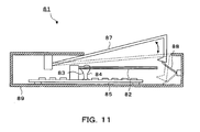
- a piezoelectric switch 81 comprises a piezoelectric device 82, lead wires 83 and 84 and a signal generating circuit 85 as shown in Fig. 11 .
- the piezoelectric switch 81 further comprises a switch 87 for driving the piezoelectric device 82, a switch returning spring 88 and a case 89.
- the piezoelectric device 1,31,41,61 or 91 is utilized as the piezoelectric device 82.
- the piezoelectric switch 81 is arranged so that the cantilever of the piezoelectric device 82 can be bent by applying a force to the free end of the piezoelectric device 82 using the switch 87.
- the switch 87 is constructed of a member having a substantially L-like shape in section and a holding member for holding one end thereof in a swingable manner.
- a ordinary state a state that the switch 87 is not operated
- the one end of the switch 87 is in contact with the switch returning spring 88 and is energized thereby so that a bent portion (a bent and angled portion) of the switch 87 protrudes out of the case 89 as shown in Fig. 11 .
- the switch returning spring 88 receives the external force from the switch 87 and is bent.
- the switch 87 is released from the pressing force, the switch 87 is allowed to return to the previous ordinary state.
- the switch 87 and the switch returning spring 88 integrally constitutes a push-on/off type manual switch.
- the switch 87 has a projection that comes into contact with the free end of the piezoelectric device 82 and bends the piezoelectric device 82.
- the signal generating circuit 85 is a circuit that converts a voltage, which is generated by the piezoelectric device 82 and taken out from the pair of conductive members through the lead wires 83 and 84, into an electric signal.
- the piezoelectric device 82 By arranging as described above, even when the piezoelectric device 82 is bent due to an impact of an external force or by an external force, the piezoelectric device 82 is not extremely deformed. Therefore, the surface of the piezoelectric element is prevented from being cracked or causing a breakage of the piezoelectric switch 81. Even when the surface of the piezoelectric element gets a crack and the electrode is divided, the area of the element contributing to the generation of electricity can be preserved, and thus a satisfactory electric signal can be obtained as the switch. Moreover, the piezoelectric device 82 has a structure such that a piece of piezoelectric member having a plate-like shape is sandwiched by the two pieces of the conductive members. Therefore, the piezoelectric element is prevented from warping, and thus the piezoelectric switch 81, which is easy to manufacture and hardly broken, can be achieved.
- the operation of the piezoelectric switch 81 will be described below.
- the switch 87 is in a state pushed up by the switch returning spring 88.
- the projection is positioned above the free end of the piezoelectric device 82.
- the projection of the switch 87 comes into contact with the free end of the piezoelectric device 82 and bends the piezoelectric device 82 downward.
- the switch 87 can be pressed down until the switch returning spring 88 is brought into contact with a bottom plate of the case 89. While the switch 87 is pressed down to the bottom end, the free end of the piezoelectric device 82 is released from the projection of the switch 87. Thereby, the piezoelectric device 82 begins to vibrate freely, and then the free vibration decreases to stop.
- the switch 87 After the switch 87 has pressed down to the bottom end, when the force pressing the switch 87 is removed, the switch 87 is pressed up by the switch returning spring 88 to return to the previous ordinary state. At this time, the projection of the switch 87 comes into contact with the piezoelectric device 82 again and bends the piezoelectric device 82 upward. And then, the free end of the piezoelectric device 82 is released from the projection. Thereby, the piezoelectric device 82 begins to vibrate freely again, and then the free vibration of the piezoelectric device 82 decreases to return to the previous ordinary state.
- the piezoelectric body when the piezoelectric device 82 is bent and allowed to vibrate freely, the piezoelectric body generates a voltage owing to the piezoelectric effect (mainly, lateral effect (d31 mode)).
- the piezoelectric device 82 When the switch 87 is pressed once and allowed to return to the previous ordinary state, the piezoelectric device 82 performs free vibration twice. Therefore, the piezoelectric device 82 outputs two alternating waveforms including a time-interval therebetween. The period of the time-interval between the alternating waveforms varies depending on the period of time the switch 87 is held in the pressed state.
Landscapes
- General Electrical Machinery Utilizing Piezoelectricity, Electrostriction Or Magnetostriction (AREA)
- Piezo-Electric Or Mechanical Vibrators, Or Delay Or Filter Circuits (AREA)
Abstract
Applications Claiming Priority (2)
| Application Number | Priority Date | Filing Date | Title |
|---|---|---|---|
| JP2004243919A JP3866258B2 (ja) | 2004-08-24 | 2004-08-24 | 圧電デバイスおよびこれを備える圧電スイッチ |
| PCT/JP2005/012783 WO2006022084A1 (ja) | 2004-08-24 | 2005-07-11 | 圧電デバイスおよびこれを備える圧電スイッチ |
Publications (3)
| Publication Number | Publication Date |
|---|---|
| EP1796256A1 EP1796256A1 (en) | 2007-06-13 |
| EP1796256A4 EP1796256A4 (en) | 2009-12-09 |
| EP1796256B1 true EP1796256B1 (en) | 2012-05-30 |
Family
ID=35967304
Family Applications (1)
| Application Number | Title | Priority Date | Filing Date |
|---|---|---|---|
| EP05757801A Not-in-force EP1796256B1 (en) | 2004-08-24 | 2005-07-11 | Piezoelectric device and piezoelectric switch employing same |
Country Status (5)
| Country | Link |
|---|---|
| US (1) | US7535155B2 (ja) |
| EP (1) | EP1796256B1 (ja) |
| JP (1) | JP3866258B2 (ja) |
| TW (1) | TW200614554A (ja) |
| WO (1) | WO2006022084A1 (ja) |
Families Citing this family (27)
| Publication number | Priority date | Publication date | Assignee | Title |
|---|---|---|---|---|
| DE602006009761D1 (de) * | 2006-03-28 | 2009-11-26 | Infineon Technologies Sensonor | Vorrichtung zum Sammeln von Energie |
| JP2008067451A (ja) * | 2006-09-05 | 2008-03-21 | Taiheiyo Cement Corp | エネルギー変換装置 |
| US7948153B1 (en) * | 2008-05-14 | 2011-05-24 | Sandia Corporation | Piezoelectric energy harvester having planform-tapered interdigitated beams |
| JP5510448B2 (ja) * | 2009-03-18 | 2014-06-04 | 富士通株式会社 | 圧電発電装置 |
| FR2946458B1 (fr) * | 2009-06-04 | 2011-07-08 | St Microelectronics Rousset | Procede de generation d'energie electrique dans un circuit integre, circuit integre correspondant et procede de fabrication |
| US8777863B2 (en) * | 2009-06-10 | 2014-07-15 | Cardiac Pacemakers, Inc. | Implantable medical device with internal piezoelectric energy harvesting |
| US20100317978A1 (en) * | 2009-06-10 | 2010-12-16 | Maile Keith R | Implantable medical device housing modified for piezoelectric energy harvesting |
| US8506495B2 (en) * | 2009-06-10 | 2013-08-13 | Cardiac Pacemakers, Inc. | Implantable medical devices with piezoelectric anchoring member |
| JP4826660B2 (ja) * | 2009-07-21 | 2011-11-30 | 株式会社村田製作所 | 圧電発電装置 |
| JP5614026B2 (ja) * | 2009-11-06 | 2014-10-29 | 株式会社村田製作所 | アクチュエータ |
| KR20110082420A (ko) * | 2010-01-11 | 2011-07-19 | 삼성전자주식회사 | 초전 재료를 이용한 에너지 수확 장치 |
| KR101451697B1 (ko) * | 2010-05-24 | 2014-10-16 | 도쿠리츠교세이호징 붓시쯔 자이료 겐큐키코 | 표면 응력 센서 |
| JP2011004598A (ja) * | 2010-09-03 | 2011-01-06 | Seiko Epson Corp | 圧電型発電機および圧電型発電機を用いた電子機器 |
| JP5685719B2 (ja) * | 2010-10-01 | 2015-03-18 | パナソニックIpマネジメント株式会社 | 振動発電素子およびそれを用いた振動発電装置 |
| CN103238271B (zh) * | 2010-12-01 | 2015-08-26 | 株式会社村田制作所 | 压电发电装置及其制造方法 |
| JP5520239B2 (ja) * | 2011-02-01 | 2014-06-11 | パナソニック株式会社 | 発電デバイスおよびそれを用いた発電モジュール |
| WO2012105368A1 (ja) * | 2011-02-04 | 2012-08-09 | 株式会社村田製作所 | 圧電発電装置 |
| US9525365B2 (en) | 2012-11-19 | 2016-12-20 | Panasonic Intellectual Property Management Co., Ltd. | Power-generating device with vibration plate that applies compressive stress to the piezoelectric layer when the vibration plate does not vibrate |
| CN104167955A (zh) * | 2013-05-16 | 2014-11-26 | 香港理工大学 | 压电元件和压电能量收集系统 |
| KR102142526B1 (ko) | 2013-09-17 | 2020-08-07 | 삼성전자주식회사 | 압전 소자 및 그 제조방법 |
| US10050565B2 (en) | 2014-09-01 | 2018-08-14 | Samsung Electro-Mechanics Co., Ltd. | Piezoelectric energy harvester and wireless switch including the same |
| US9876445B2 (en) | 2014-09-01 | 2018-01-23 | Samsung Electro-Mechanics Co., Ltd. | Piezoelectric energy harvester and wireless switch including the same |
| KR101578321B1 (ko) * | 2015-01-21 | 2015-12-16 | 성균관대학교산학협력단 | 온도변화에 의해 에너지를 발생시키는 에너지 발생소자 및 이를 포함하는 온도변화 감지센서 |
| JP6876960B2 (ja) * | 2017-03-29 | 2021-05-26 | パナソニックIpマネジメント株式会社 | 発電装置及びそれを備えた入力装置 |
| CN111066165B (zh) * | 2017-07-05 | 2023-09-26 | 格勒诺布尔阿尔卑斯大学 | 压电能量收集的弯曲结构及其制造方法 |
| JP6539796B1 (ja) * | 2019-01-11 | 2019-07-03 | 誠 勝部 | 発電装置及び携帯型パーソナルコンピュータ |
| JP7508056B1 (ja) | 2023-11-08 | 2024-07-01 | コフロック株式会社 | バルブインジケーター |
Citations (2)
| Publication number | Priority date | Publication date | Assignee | Title |
|---|---|---|---|---|
| US6144142A (en) * | 1998-11-06 | 2000-11-07 | Face International Corp. | Multi-layer piezoelectric transformer mounting device |
| US20030193417A1 (en) * | 2001-07-03 | 2003-10-16 | Face Bradbury R. | Self-powered switch initiation system |
Family Cites Families (24)
| Publication number | Priority date | Publication date | Assignee | Title |
|---|---|---|---|---|
| US3500451A (en) * | 1967-06-29 | 1970-03-10 | Gen Telephone & Elect | Piezoelectric voltage generator |
| US4136312A (en) * | 1976-12-30 | 1979-01-23 | Westinghouse Electric Corp. | Method and apparatus for detection of rotor faults in dynamoelectric machines |
| JPS5683983A (en) | 1979-12-12 | 1981-07-08 | Sony Corp | Electricity-machinery conversion element |
| US4387318A (en) * | 1981-06-04 | 1983-06-07 | Piezo Electric Products, Inc. | Piezoelectric fluid-electric generator |
| JPS5932182A (ja) * | 1982-08-16 | 1984-02-21 | Sumitomo Special Metals Co Ltd | バイモルフ用圧電素子 |
| US4769882A (en) * | 1986-10-22 | 1988-09-13 | The Singer Company | Method for making piezoelectric sensing elements with gold-germanium bonding layers |
| US5213212A (en) * | 1989-05-18 | 1993-05-25 | The United States Of America As Represented By The Secretary Of The Navy | Magnetic stabilization of spooled fiber optic data links |
| JPH0746388A (ja) | 1993-07-30 | 1995-02-14 | Fujitsu Ltd | データ通信装置 |
| JPH09205781A (ja) | 1995-02-01 | 1997-08-05 | Seiko Epson Corp | 圧電体発電装置及びこれを備えた携帯型電力供給装置、携帯型電子機器 |
| US5814921A (en) * | 1995-03-13 | 1998-09-29 | Ocean Power Technologies, Inc. | Frequency multiplying piezoelectric generators |
| JPH09211151A (ja) | 1996-01-30 | 1997-08-15 | Seiko Epson Corp | 発電装置、携帯型機器および圧電体の製造方法 |
| DE19818449A1 (de) * | 1998-04-24 | 1999-11-04 | Siemens Ag | Piezoelektrischer Biegewandler und Modul aus einer Anzahl von piezoelektrischen Biegewandlern |
| US6028382A (en) * | 1998-07-14 | 2000-02-22 | Reliance Electrical Industrial Company | Temperature sensing arrangement for the stator core of an electromechanical machine |
| US6252336B1 (en) * | 1999-11-08 | 2001-06-26 | Cts Corporation | Combined piezoelectric silent alarm/battery charger |
| US6630894B1 (en) * | 2000-07-14 | 2003-10-07 | Face International Corp. | Self-powered switching device |
| JP2002141576A (ja) * | 2000-11-02 | 2002-05-17 | Fujitsu Ltd | ピエゾ素子と電極との接合方法及び該接合方法を使用したピエゾマイクロアクチュエータ |
| JP2003007491A (ja) * | 2001-06-26 | 2003-01-10 | Nec Tokin Ceramics Corp | 発光体点灯装置 |
| JP2003218418A (ja) * | 2002-01-18 | 2003-07-31 | Matsushita Electric Ind Co Ltd | 圧電型発電器 |
| WO2004023572A1 (en) * | 2002-08-30 | 2004-03-18 | Usc Corporation | Piezoelectric generator |
| JP4513252B2 (ja) | 2002-10-25 | 2010-07-28 | パナソニック株式会社 | 圧電体薄膜素子およびそれを用いたアクチュエータ、インクジェットヘッドならびにインクジェット記録装置 |
| CN100411214C (zh) * | 2003-12-16 | 2008-08-13 | 松下电器产业株式会社 | 压电体薄膜装置和压电体薄膜装置的驱动方法 |
| JP4451219B2 (ja) * | 2004-06-03 | 2010-04-14 | 日本電波工業株式会社 | 水晶振動子 |
| WO2006009540A1 (en) * | 2004-06-19 | 2006-01-26 | Face Bradbury R | Self-powered switch initiation system |
| WO2007061610A1 (en) * | 2005-11-18 | 2007-05-31 | Par Technologies, Llc | Human powered piezoelectric power generating device |
-
2004
- 2004-08-24 JP JP2004243919A patent/JP3866258B2/ja not_active Expired - Fee Related
-
2005
- 2005-07-11 US US11/660,666 patent/US7535155B2/en not_active Expired - Fee Related
- 2005-07-11 EP EP05757801A patent/EP1796256B1/en not_active Not-in-force
- 2005-07-11 WO PCT/JP2005/012783 patent/WO2006022084A1/ja active Application Filing
- 2005-08-17 TW TW094128006A patent/TW200614554A/zh unknown
Patent Citations (2)
| Publication number | Priority date | Publication date | Assignee | Title |
|---|---|---|---|---|
| US6144142A (en) * | 1998-11-06 | 2000-11-07 | Face International Corp. | Multi-layer piezoelectric transformer mounting device |
| US20030193417A1 (en) * | 2001-07-03 | 2003-10-16 | Face Bradbury R. | Self-powered switch initiation system |
Also Published As
| Publication number | Publication date |
|---|---|
| WO2006022084A1 (ja) | 2006-03-02 |
| EP1796256A1 (en) | 2007-06-13 |
| US20070252479A1 (en) | 2007-11-01 |
| US7535155B2 (en) | 2009-05-19 |
| JP2006067643A (ja) | 2006-03-09 |
| TW200614554A (en) | 2006-05-01 |
| EP1796256A4 (en) | 2009-12-09 |
| JP3866258B2 (ja) | 2007-01-10 |
Similar Documents
| Publication | Publication Date | Title |
|---|---|---|
| EP1796256B1 (en) | Piezoelectric device and piezoelectric switch employing same | |
| US5849125A (en) | Method of manufacturing flextensional transducer using pre-curved piezoelectric ceramic layer | |
| US5831371A (en) | Snap-action ferroelectric transducer | |
| JP4035156B2 (ja) | 超音波アクチュエータ | |
| JP4679938B2 (ja) | 超音波モータ | |
| US6060811A (en) | Advanced layered composite polylaminate electroactive actuator and sensor | |
| US5404067A (en) | Bonded piezoelectric bending transducer and process for producing the same | |
| JP4069161B2 (ja) | 圧電素子及び超音波アクチュエータ | |
| US10069440B2 (en) | Vibrator and ultrasonic motor | |
| JP2001326399A (ja) | アクチュエータ装置 | |
| JP2006311647A (ja) | 超音波モータ | |
| JPH08242025A (ja) | 圧電アクチュエータ | |
| US6140745A (en) | Motor mounting for piezoelectric transducer | |
| US8076823B2 (en) | Ultrasonic actuator | |
| US6411010B1 (en) | Piezoelectric actuator | |
| JP3535111B2 (ja) | 圧電アクチュエータ | |
| JP3444504B2 (ja) | 超音波振動子 | |
| JPS6412111B2 (ja) | ||
| JP4443707B2 (ja) | 圧電アクチュエータ | |
| JPH08251954A (ja) | 超音波振動子 | |
| JP2003101093A (ja) | 圧電アクチュエータ | |
| WO2002091492A2 (en) | Electrostrictive bending transducer | |
| JPH02206185A (ja) | 圧電アクチュエータ | |
| JP2533861B2 (ja) | 圧電アクチユエ−タ | |
| JPH09140170A (ja) | 振動アクチュエータ |
Legal Events
| Date | Code | Title | Description |
|---|---|---|---|
| PUAI | Public reference made under article 153(3) epc to a published international application that has entered the european phase |
Free format text: ORIGINAL CODE: 0009012 |
|
| 17P | Request for examination filed |
Effective date: 20070321 |
|
| AK | Designated contracting states |
Kind code of ref document: A1 Designated state(s): DE ES FR GB IT NL |
|
| DAX | Request for extension of the european patent (deleted) | ||
| RBV | Designated contracting states (corrected) |
Designated state(s): DE ES FR GB IT NL |
|
| RIN1 | Information on inventor provided before grant (corrected) |
Inventor name: ISHIKAWA, KATSUYUKILOT55, BAKER ARANG INDUSTRIAL E |
|
| A4 | Supplementary search report drawn up and despatched |
Effective date: 20091106 |
|
| 17Q | First examination report despatched |
Effective date: 20100408 |
|
| GRAP | Despatch of communication of intention to grant a patent |
Free format text: ORIGINAL CODE: EPIDOSNIGR1 |
|
| GRAS | Grant fee paid |
Free format text: ORIGINAL CODE: EPIDOSNIGR3 |
|
| RAP1 | Party data changed (applicant data changed or rights of an application transferred) |
Owner name: TAIHEIYO CEMENT CORPORATION |
|
| GRAA | (expected) grant |
Free format text: ORIGINAL CODE: 0009210 |
|
| AK | Designated contracting states |
Kind code of ref document: B1 Designated state(s): DE ES FR GB IT NL |
|
| REG | Reference to a national code |
Ref country code: GB Ref legal event code: FG4D |
|
| REG | Reference to a national code |
Ref country code: DE Ref legal event code: R096 Ref document number: 602005034431 Country of ref document: DE Effective date: 20120802 |
|
| REG | Reference to a national code |
Ref country code: NL Ref legal event code: VDEP Effective date: 20120530 |
|
| PG25 | Lapsed in a contracting state [announced via postgrant information from national office to epo] |
Ref country code: NL Free format text: LAPSE BECAUSE OF FAILURE TO SUBMIT A TRANSLATION OF THE DESCRIPTION OR TO PAY THE FEE WITHIN THE PRESCRIBED TIME-LIMIT Effective date: 20120530 |
|
| PG25 | Lapsed in a contracting state [announced via postgrant information from national office to epo] |
Ref country code: IT Free format text: LAPSE BECAUSE OF FAILURE TO SUBMIT A TRANSLATION OF THE DESCRIPTION OR TO PAY THE FEE WITHIN THE PRESCRIBED TIME-LIMIT Effective date: 20120530 |
|
| PLBE | No opposition filed within time limit |
Free format text: ORIGINAL CODE: 0009261 |
|
| STAA | Information on the status of an ep patent application or granted ep patent |
Free format text: STATUS: NO OPPOSITION FILED WITHIN TIME LIMIT |
|
| GBPC | Gb: european patent ceased through non-payment of renewal fee |
Effective date: 20120830 |
|
| REG | Reference to a national code |
Ref country code: FR Ref legal event code: ST Effective date: 20130329 |
|
| PG25 | Lapsed in a contracting state [announced via postgrant information from national office to epo] |
Ref country code: FR Free format text: LAPSE BECAUSE OF NON-PAYMENT OF DUE FEES Effective date: 20120731 Ref country code: ES Free format text: LAPSE BECAUSE OF FAILURE TO SUBMIT A TRANSLATION OF THE DESCRIPTION OR TO PAY THE FEE WITHIN THE PRESCRIBED TIME-LIMIT Effective date: 20120910 |
|
| 26N | No opposition filed |
Effective date: 20130301 |
|
| REG | Reference to a national code |
Ref country code: DE Ref legal event code: R097 Ref document number: 602005034431 Country of ref document: DE Effective date: 20130301 |
|
| PG25 | Lapsed in a contracting state [announced via postgrant information from national office to epo] |
Ref country code: GB Free format text: LAPSE BECAUSE OF NON-PAYMENT OF DUE FEES Effective date: 20120830 |
|
| PGFP | Annual fee paid to national office [announced via postgrant information from national office to epo] |
Ref country code: DE Payment date: 20130722 Year of fee payment: 9 |
|
| REG | Reference to a national code |
Ref country code: DE Ref legal event code: R119 Ref document number: 602005034431 Country of ref document: DE |
|
| PG25 | Lapsed in a contracting state [announced via postgrant information from national office to epo] |
Ref country code: DE Free format text: LAPSE BECAUSE OF NON-PAYMENT OF DUE FEES Effective date: 20150203 |
|
| REG | Reference to a national code |
Ref country code: DE Ref legal event code: R119 Ref document number: 602005034431 Country of ref document: DE Effective date: 20150203 |