EP1792402B1 - Strukturen zur digital-analog-wandlung - Google Patents
Strukturen zur digital-analog-wandlung Download PDFInfo
- Publication number
- EP1792402B1 EP1792402B1 EP05774067A EP05774067A EP1792402B1 EP 1792402 B1 EP1792402 B1 EP 1792402B1 EP 05774067 A EP05774067 A EP 05774067A EP 05774067 A EP05774067 A EP 05774067A EP 1792402 B1 EP1792402 B1 EP 1792402B1
- Authority
- EP
- European Patent Office
- Prior art keywords
- dac
- resistor ladder
- word
- resistor
- legs
- Prior art date
- Legal status (The legal status is an assumption and is not a legal conclusion. Google has not performed a legal analysis and makes no representation as to the accuracy of the status listed.)
- Not-in-force
Links
Images


Classifications
-
- H—ELECTRICITY
- H03—ELECTRONIC CIRCUITRY
- H03M—CODING; DECODING; CODE CONVERSION IN GENERAL
- H03M1/00—Analogue/digital conversion; Digital/analogue conversion
- H03M1/10—Calibration or testing
- H03M1/1009—Calibration
- H03M1/1033—Calibration over the full range of the converter, e.g. for correcting differential non-linearity
- H03M1/1057—Calibration over the full range of the converter, e.g. for correcting differential non-linearity by trimming, i.e. by individually adjusting at least part of the quantisation value generators or stages to their nominal values
-
- H—ELECTRICITY
- H03—ELECTRONIC CIRCUITRY
- H03M—CODING; DECODING; CODE CONVERSION IN GENERAL
- H03M1/00—Analogue/digital conversion; Digital/analogue conversion
- H03M1/66—Digital/analogue converters
- H03M1/74—Simultaneous conversion
- H03M1/78—Simultaneous conversion using ladder network
- H03M1/785—Simultaneous conversion using ladder network using resistors, i.e. R-2R ladders
Definitions
- the present invention relates to digital-to-analog converters (DACs) and in particular to DAC structures implemented using resistive ladder configurations.
- DACs digital-to-analog converters
- the invention more particularly relates to DAC structures based on an R-2R configuration.
- DAC structures are well known in the art. They are used to convert an input digital signal, usually provided in the form of a binary code, to an analog output signal- either in the form of a corresponding voltage or current. This is achieved using switches or a network of resistors or current sources.
- USP '174 describes an R-2R ladder structure which includes a plurality of legs. Each leg contributes towards the resolution of the device, such that the more legs that are provided in the structure the better the resolution.
- a plurality of corresponding switches which need to be scaled appropriately. The addition of switches is not a trivial activity, as each new switch needs to be scaled appropriately to the preceding switch.
- a further issue with high resolution DACs is that the linearity and monotonicity of the DAC is limited by component matching. Random component mismatch can reduce the monotonicity and linearity of the DAC structure. This problem has traditionally been countered either by laser trimming components to adjust their values or by incorporating calibration circuitry on board.
- JP2001 127634 discloses a DAC which comprises a first conversion circuit and a second conversion circuit.
- the first conversion circuit is driven by lower order bits b0-b5 and comprises an R2R ladder.
- the second conversion circuit is driven by high order bits b6, b7 and comprises a weight resistance system employing a weigh unit R.
- JP11017547 discloses a DAC which comprises a first conversion circuit and a second conversion circuit.
- the first conversion circuit comprises an R2R ladder for converting the LSBs of a digital word, bit switches and constant current sources providing a constant current I.
- the second conversion circuit comprises an R2R ladder and constant current sources providing a constant current 21, and a bit converter.
- the bit converter converts the input of higher two bits into the value of three bits, controls the switches and adds together the currents 21 in sequence. As the numbers of bits in charge of both conversion circuits can be freely changed, the high conversion accuracy is secured.
- a first embodiment of the invention provides a digital-to-analog converter as detailed in claim 1.
- the invention also provides a method as detailed in claim 17.
- Advantageous embodiments are provided in the dependent claims.
- the ladder may typically be provided in a R-2R topology or modified version thereto.
- some of the link 'R' resistors are removed and the remaining DAC resistors scaled. This increases the impedance of the first component or lower DAC section at the expense of resistor area but reduces the current flowing in the DAC and also reduces the effect of switch and wiring non-idealities relative to the resistor value in the lower part of the DAC.
- the present invention provides for a minimization of the total DAC area for a given resolution and reduces the switch scaling problem.
- Such an injection may be added to any node of the ladder but typically is coupled to the top of a termination resistor.
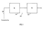
- a digital-to-analog converter 100 adapted to convert an input digital signal to an analog output signal.
- the converter includes an upper part 105 that is responsible for converting a first portion of the digital input word comprising the most significant bit (MSB) of the digital input word and a lower part 110 responsible for converting the remaining portion (i.e. the least significant bits LSBs) of the digital input word.
- the resistance of the upper part, R2 can be less than that of the resistance of the lower part, R1.
- the DAC of the present invention converts an input word to a single analog output corresponding to that input word.
- the input word can be considered as being divisible into two sub-words: a first sub-word containing the least significant bits (LSBs) of the input word and the second sub-word containing the most significant bits (MSBs) of the input word, each of the two sub-words being converted by a part of the DAC.
- the lower part not only provides the corresponding analog output voltage signal for the LSB of the input word but also may be used to tune the upper part.
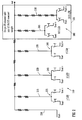
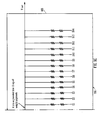
- the upper portion 105 includes a first set of segments 200, shown here as two segments 205, 210.
- the lower part is provided as three legs 215, 220, 225 in a traditional R-2R configuration, with each leg of the lower part providing 1, 2 or 4 LSBs contributing towards the output of the DAC.
- a termination leg 230 is coupled to Vref-, typically a ground signal.
- Each of the three legs of the lower part are switchably coupled via switches 235, 240, 245 respectively between Vref- and Vref+.
- the effect of switching each segment of the set of the upper part on the output of the DAC corresponds to the effect of switching multiples of one bit from the lower part of the digital input word (which is equivalent to a weighting less than one LSB of the upper part of the word)
- the first segment is provided with a weighting of 8/3 LSBs and the second a weighting of 16/3 LSBs (being equivalent to 1 /3 and 2/3 the nominal weight of the bit of the upper part of the word).
- the effect is equal to 8 LSB as in a standard R- 2R arrangement.
- the code loaded to the LSB section of the DAC can be modified to correct the output, i.e. load 10001 for code 7 instead of code 10010 to correct for an error of +1 LSB DNL.
- This basic scheme can be extended to calibrate high resolution DACs.
- the legs of the lower part of the DAC are used to tune the output of the DAC when a segment from the set of the upper part has been selected.
- the calibration algorithm that is used is such to ensure that the lower part is never implemented in full deflection, -i.e. that the legs of the lower part are either all on or all off.
- the legs of the lower part may be used to tune or adapt the contribution from the segments of the upper part to provide the desired output from the DAC for the input digital word, and preferably can be used to ensure that there is no deviation from +DNL ⁇ 1 LSB
- the lower part is preferably provided in a ladder configuration.
- the present invention also provides for modifications to such conventional ladder configurations.
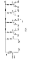
- a modification of a standard R-2R structure shown in Figure 3 , some of the link 'R' resistors, between adjacent legs, are removed and the remaining DAC resistors scaled, i.e. those resistors provided on the legs of the ladder between the termination leg and the removed resistor.
- the number of resistors is increased twofold so that there is provided a 2R-4R configuration.
- the lower part of the DAC is preferably provided with a termination leg, the termination leg being directly coupled to a reference signal, typically ground. It is also known to couple the termination leg of such ladder configurations to ground via a switch, but in accordance with preferred embodiments of the present invention, the coupling is direct as opposed to via the switch.
- a modification to a ladder configuration is provided where in the ladder is additionally coupled to a current source 400, the current source being configured to inject a scaled current (related to the reference) into a node of the R- 2R ladder.
- a scaled current (related to the reference) into a node of the R- 2R ladder.
- Such an injection may be added to any node of the ladder but typically is coupled to the top of a termination resistor, as is shown in Figure 4 . It is preferable to couple the current source to the termination leg as the available headroom within the DAC architecture is greatest here and as such it is easier to design the current source.
- R-2R DAC ladder architecture enables one to extend the resolution of the R-2R DAC without increasing the number of resistors and switches. This serves to extend the resolution provided by such architectures. It will be appreciated that the value of the current injected into the termination leg is typically of the order of microamps, whereas if the current was injected into other legs of the ladder, a signal of much reduced magnitudes would typically be required.
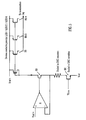
- FIG. 5 shows an example of the type of current source circuit that may be used in implementations of DACs according to the present invention. It will be appreciated however that the structure and components illustrated are exemplary of the type of configuration that may be considered by a person skilled in the art to provide a current injection to the resistor ladder of Figure 4 .
- an amplifier A is provided whose non-inverting input is coupled to Vref+.
- the inverting input is coupled in a feedback configuration to a resistor and a switch Q2, the values of which are scaled to the values of the switches and resistors in the legs of the lower part of the DAC.
- the gate of the switch Q2 is controlled by a bias voltage Vbias, so as to achieve the scaling effect.
- the output of the amplifier controls the gate of a second switch Q1, the source of which controls a master MOSFET device of a mirror arrangement.
- the mirror is adapted to provide for the selective coupling of currents- shown here as B0, B0/2 and B0/4 into the termination leg of the lower part of the DAC- not shown in this Figure, but were previously shown in Figure 3 .
- the selective switching achieves the injection of current equivalent of 1 LSB, 1 LSB/2 and 1 LSB/4 respectively.
- Such injection of current is advantageous in that it improves the resolution of the DAC without requiring additional legs within the resistor ladder DAC arrangement.
- any one of the three embodiments may be used independently of the others, but in preferred implementations all three are combined.
- Such an example is shown in the architecture of Figure 6 .
- Figure 6 has been subdivided into three sheets shown as Figures 6A , 6B and 6C . These can be read in conjunction with one another to view the entire DAC structure.
- the upper part 105 is adapted to provide 4 bits of the input word.
- the lower part of the DAC is provided as a modified R-2R architecture with the link resistor between the lower part and the upper part removed, such that the lower legs (legs B1-B11), (i.e. those legs below the region where the link resistor traditionally would have been found), scaled to provide a 2R-4R architecture.
- the four bits after the segments B11, B10, B9, B8 are alternatively split into the nominal weighting sets of Figure 2 , shown here as 1/3 and 2/3 nominal weighting arrangements.
- the following seven bits (B7...B1) are provided as a standard 2R-4R implementation.
- Bit 0 and weights of LSB/2 and LSB/4 are generated by coupling the termination leg to a current source and using the current source to inject currents into the mid point of that leg, i.e. in the mid point of the 4 resistors provided the termination leg.
- the weights less than 1 LSB are adapted to give extra resolution to the DAC if so required.
- each of the legs (B0-B11 and S0-S14) are switchably coupled to a voltage reference, as is normal for resistor ladder configurations, but for the sake of convenience the individual switch components are not shown.
- the teaching herein provides for an improved DAC architecture where the improvements may be provided independently or in combination with one another.
- This teaching is specifically adapted to provide a DAC structure optimized for digital calibration. The goal is achieved this by providing a DAC structure comprising an upper part defining a main part of the DAC architecture and a lower part defining a subDAC part of the architecture.
- the subDAC part is used to provide a tuning of the upper part of the DAC so as to ensure that for increasing input code applied to the DAC, the DAC provides an output which does not vary by more than 1 LSB. This is achieved by selective switching of the upper and lower parts of the DAC together.
- the underlying DAC architecture should have resolution greater than the desired resolution of the calibrated output and should also have a means of guaranteeing that there are no gaps in the transfer function (i.e., a means of ensuring no positive DNL errors > 1 LSB). These requirements are met by the architectures discussed herein.
- Figure 7 shows a schematic of a DAC calibration system 700 provided for practicing the invention.
- the system provides an apparatus & method for generating a linear, resistor ladder, voltage output DAC in the presence of component matching errors.
- a sixteen bit user input word is provided at a interface decode 705, where the MSBs and LSBs of the word are separated.
- the DAC 700 including a main-section 710 converting the MSBs of the DAC word into an output voltage and a sub-section 715 converting the LSBs of the DAC word.
- the sections are coupled together to provide an overall output voltage at an output 720.
- the main-section 710 may be provided in a configuration, such as that shown in Figure 6 as block 105, containing a resistor ladder structured so that it's LSB is less than full-scale of the sub-section 715 but substantially greater than both the LSB of the sub-section & the overall DAC transfer function LSB.
- the sub-section 715 also containing a resistor ladder structure, an example of the type of structure being shown as block 110 in Figure 6 .
- the ladder structures of the main-section is arranged and the sub-section is scaled so that (in the absence of mismatch) all voltage points in the DAC transfer function (except zero scale (ZS) and full scale (FS)) can be obtained without loading ZS or FS to the sub-section DAC. In this manner it will be apparent that the sub-section DAC uses a reduced code range.
- the interface decode is structured to select a main-section & sub-section DAC word for every user input code (except full scale) so that when a main-section code is selected the sub-section is not at zero-scale or full scale.
- a calibration memory 725 which stores error corrections for each segment of the main-section, is also provided. Selected corrections from the data stored in this memory may be added for each segment of the main-section selected to the LSB word using an adder 730.
- the error in the segments of the main section is measured and corresponding corrections stored in the memory 725. These corrections are then automatically added to the code loaded to the sub-section depending on the main-section code loaded (i.e. the segments selected in the ladder of the main section).
- the present invention provides a DAC configuration that can be used to convert a digital input word into an analog voltage output.
- the illustrated embodiments and principles of operation have been described with reference to an upper and a lower part or a first and second component but it will be appreciated that such nomenclature is used for ease of explanation and it is not intended to limit the protection in any way except as may be deemed necessary in the light of the appended claims. Similarly modifications can be made and will be apparent to those skilled in the art to the exemplary embodiments described herein without departing from the spirit and scope of the present invention.
Claims (17)
- Digital-/Analog-Wandler (DAC), der dazu eingerichtet ist, ein digitales Eingangswort in ein analoges Ausgangsspannungssignal zu wandeln, wobei das digitale Eingangswort in einen oberen und einen unteren Teil teilbar ist, und der DAC enthält: einen ersten Widerstandsleiter-DAC, der vom unteren Teil des Wortes gesteuert wird und eine Ausgangsspannung erzeugt, und einen zweiten Widerstandsleiter-DAC, der vom oberen Teil des Wortes gesteuert wird und eine Ausgangsspannung erzeugt, wobei der erste Widerstandsleiter-DAC eine Mehrzahl binärer gewichteter Zweige und der zweite Widerstandsleiter-DAC mindestens zwei diskrete Segmente aufweist, wobei jedes diskrete Segment eine Gewichtung entsprechend den Mehrfachen eines Bit des unteren Teils des Wortes hat und die mindestens zwei diskreten Segmente der Nenngewichtung des entsprechenden Bit des oberen Teils des Wortes entsprechend,
dadurch gekennzeichnet, dass:eine Schaltsequenz, die aus einer Kalibrierungsphase abgeleitet ist, die Zweige des ersten Widerstandsleiter-DAC und die Segmente des zweiten Widerstandsleiter-DAC so steuert, dass die Ausgangsspannung des DAC in einem gewünschten Wert resultiert, wobei die Schaltsequenz verschieden von der Schaltsequenz des ursprünglichen digitalen Eingangswortes ist undsicherstellt, dass der untere Teil des Wortes niemals in voller Ablenkung implementiert wird. - DAC nach Anspruch 1, bei dem die Gewichtung mindestens eines der Segmente des zweiten Widerstandsleiter-DAC geringer ist als die Gesamt-Gewichtung des unteren Teils des Wortes.
- DAC nach Anspruch 1, bei dem die Leiter des ersten Widerstandsleiter-DAC eine R-2R-Architektur hat.
- DAC nach Anspruch 3, bei dem die Leiter des ersten Widerstandsleiter-DAC eine skalierte R-2R-Architektur mit Zweigen mit einer Mehrzahl Widerständen aufweist, wobei die Zweige durch Verbindungswiderstände getrennt sind.
- DAC nach Anspruch 4, bei dem mindestens einer der Verbindungswiderstände im Vergleich zu einer herkömmlichen R-2R-Architektur entnommen ist und die übrigen Zweigwiderstände entsprechend dieser Entnahme skaliert sind.
- DAC nach Anspruch 1, bei dem der erste Widerstandsleiter-DAC mit einem Abschlusszweig versehen ist, wobei der Abschlusszweig direkt mit einem Referenzsignal gekoppelt ist.
- DAC nach Anspruch 1, bei dem der erste Widerstandsleiter-DAC mit einer Stromquelle gekoppelt ist, wobei die Stromquelle so konfiguriert ist, dass ein skalierter Strom in einen Knoten der Leiter injiziert wird.
- DAC nach Anspruch 7, bei dem der injizierte Strom in einen Abschlusszweig der Leiter injiziert wird.
- DAC nach Anspruch 6, bei dem der Abschlusszweig mit einer Referenzspannung gekoppelt ist und eine Mehrzahl schaltbarer Zweige vorgesehen ist, von denen ein jeder schaltbar mit einer Referenzspannung gekoppelt ist, und bei dem mindestens eines der individuellen Segmente außerdem mit einer Stromquelle gekoppelt ist, wobei die Stromquelle dazu eingerichtet ist, einen verstellbaren Strom in den ersten Widerstandsleiter-DAC zu injizieren, um die Auflösung des DAC zu erhöhen.
- DAC nach Anspruch 9, bei dem der in den ersten Widerstandsleiter-DAC injizierte Strom relativ zur Referenzspannung skaliert ist.
- DAC nach Anspruch 9, bei dem der Wert des Widerstands, der in den Zweigen des ersten Widerstandsleiter-DAC bereitgestellt wird, dem zweifachen Wert des Widerstands in den Zweigen des zweiten Widerstandsleiter-DAC entspricht.
- DAC nach Anspruch 11, bei dem ein oberer Zweig des ersten Widerstandsleiter-DAC direkt mit einem unteren Zweig des zweiten Widerstandsleiter-DAC ohne einen Kopplungswiderstand so gekoppelt ist, dass der Widerstand der Zweige im ersten Widerstandsleiter-DAC ein skaliertes Vielfaches der Zweige im zweiten Abschnitt ist.
- DAC nach Anspruch 12, bei dem mindestens ein Zweig segmentiert ist.
- DAC nach Anspruch 1, bei dem eine Schnittstellen-Decodierung so strukturiert ist, dass das erste Widerstandsleiter-DAC-Wort und das zweite Widerstandsleiter-DAC-Wort für eingegebene Benutzercodes so gewählt wird, dass dann, wenn der zweite Widerstandsleiter-DAC-Code gewählt wird, der erste Widerstandsleiter-DAC zwischen null und Vollausschlag ist, wobei die Schnittstellen-Decodierung den digitalen Eingangscode an ein MSB-DAC-Wort und ein LSB-DAC-Wort trennt; ein Kalibrierungsspeicher zum Speichern der DNL- und/oder INL-Fehlerkorrekturen für den zweiten Widerstandsleiter-DAC und ein Addierer zum Addieren der gewählten Fehlerkorrektur aus dem Kalibrierungsspeicher zum LSB-DAC-Wort vorgesehen sind.
- DAC nach Anspruch 14, bei dem der Kalibrierungsspeicher mit Fehlerkorrekturen während eines Produktionstests des DAC geladen wird.
- DAC nach Anspruch 14, bei dem der Addierer so konfiguriert ist, dass er die Korrekturen zu dem im ersten Widerstandsleiter-DAC geladenen Code bei der Wahl eines vorgegebenen Segments des zweiten Widerstandsleiter-DAC automatisch addiert.
- Verfahren zum Wandeln eines digitalen Eingangswortes in eine entsprechende Ausgangsspannung, wobei das Verfahren die Schritte enthält: Teilen des digitalen Eingangswortes in einen unteren und einen oberen Teil, Wandeln des unteren Teils des digitalen Eingangswortes in eine entsprechende Ausgangsspannung unter Verwendung eines ersten Widerstandsleiter-Digital/Analog-Wandlers (DAC), Wandeln des oberen Teils des digitalen Eingangswortes in eine entsprechende Ausgangsspannung unter Verwendung eines zweiten Widerstandsleiter-Digital/Analog-Wandlers, wobei der erste Widerstandsleiter-DAC eine Mehrzahl binärer gewichteter Zweige und der zweite Widerstandsleiter-DAC mindestens zwei diskrete Segmente aufweist, wobei jedes diskrete Segment eine Gewichtung entsprechend den Mehrfachen eines Bit des unteren Teils des Wortes hat und die mindestens zwei diskreten Segmente der Nenngewichtung des entsprechenden Bit des oberen Teils des Wortes entsprechen,
dadurch gekennzeichnet, dass:eine Schaltsequenz, die aus einer Kalibrierungsphase abgeleitet ist, die Zweige des ersten Widerstandsleiter-DAC und die Segmente des zweiten Widerstandsleiter-DAC so steuert, dass die Ausgangsspannung des DAC in einem gewünschten Wert resultiert, wobei die Schaltsequenz verschieden von der Schaltsequenz des ursprünglichen digitalen Eingangswortes ist undsicherstellt, dass der untere Teil des Wortes niemals in voller Ablenkung implementiert wird.
Applications Claiming Priority (3)
| Application Number | Priority Date | Filing Date | Title |
|---|---|---|---|
| US61146904P | 2004-09-20 | 2004-09-20 | |
| US11/048,374 US7095351B2 (en) | 2004-09-20 | 2005-02-01 | Digital-to-analog converter structures |
| PCT/EP2005/054141 WO2006032592A1 (en) | 2004-09-20 | 2005-08-23 | Digital-to-analog converter structures |
Publications (2)
| Publication Number | Publication Date |
|---|---|
| EP1792402A1 EP1792402A1 (de) | 2007-06-06 |
| EP1792402B1 true EP1792402B1 (de) | 2009-07-15 |
Family
ID=35159837
Family Applications (1)
| Application Number | Title | Priority Date | Filing Date |
|---|---|---|---|
| EP05774067A Not-in-force EP1792402B1 (de) | 2004-09-20 | 2005-08-23 | Strukturen zur digital-analog-wandlung |
Country Status (7)
| Country | Link |
|---|---|
| US (1) | US7095351B2 (de) |
| EP (1) | EP1792402B1 (de) |
| JP (1) | JP4550901B2 (de) |
| CN (1) | CN101023583B (de) |
| DE (1) | DE602005015464D1 (de) |
| TW (1) | TWI296880B (de) |
| WO (1) | WO2006032592A1 (de) |
Families Citing this family (22)
| Publication number | Priority date | Publication date | Assignee | Title |
|---|---|---|---|---|
| US7173552B1 (en) * | 2003-10-01 | 2007-02-06 | Analog Devices, Inc. | High accuracy segmented DAC |
| TWI330001B (en) * | 2006-08-15 | 2010-09-01 | Realtek Semiconductor Corp | Dynamic bias control circuit and related apparatus for digital-to-analog converter |
| US7688240B2 (en) * | 2008-05-02 | 2010-03-30 | Analog Devices, Inc. | Method and apparatus for calibrating an RDAC for end-to-end tolerance correction of output resistance |
| CN101345527B (zh) * | 2008-07-09 | 2010-06-02 | 清华大学 | 一种基于CeRAM单元的数模变换器 |
| DE102010016556A1 (de) * | 2009-04-24 | 2010-11-25 | Intersil Americas Inc., Milpitas | Widerstands-Feineinstellung für Polysilizium |
| US8164495B2 (en) * | 2009-11-12 | 2012-04-24 | Intersil Americas Inc. | Integrated non-linearity (INL) and differential non-linearity (DNL) correction techniques for digital-to-analog converters (DACS) |
| CN101834605B (zh) * | 2010-04-12 | 2013-03-06 | 智原科技股份有限公司 | 模拟数字转换器的测试系统与测试方法 |
| CN101924554B (zh) * | 2010-06-30 | 2013-07-03 | 中国电子科技集团公司第五十八研究所 | 电荷耦合流水线模数转换器的共模误差校准电路 |
| US8514112B2 (en) | 2010-07-15 | 2013-08-20 | Analog Devices, Inc. | Programmable linearity correction circuit for digital-to-analog converter |
| JP6043052B2 (ja) * | 2011-06-20 | 2016-12-14 | ティアック株式会社 | Da変換装置 |
| CN102545906B (zh) * | 2012-02-10 | 2015-01-07 | 英特格灵芯片(天津)有限公司 | 电流型数模转换方法和装置 |
| US8537043B1 (en) * | 2012-04-12 | 2013-09-17 | Analog Devices, Inc. | Digital-to-analog converter with controlled gate voltages |
| US8576101B1 (en) | 2012-11-05 | 2013-11-05 | Google Inc. | Calibration of an R2R ladder based current digital-to-analog converter (DAC) |
| US8912939B2 (en) * | 2012-12-14 | 2014-12-16 | Analog Devices Technology | String DAC leakage current cancellation |
| CN103795415A (zh) * | 2014-01-24 | 2014-05-14 | 中国人民解放军国防科学技术大学 | 基于双路组合数模转换器的高精度数模转换方法及装置 |
| CN104168026B (zh) * | 2014-08-25 | 2017-09-15 | 长沙瑞达星微电子有限公司 | 一种分段式电流舵dac电路 |
| US9276598B1 (en) * | 2015-05-22 | 2016-03-01 | Texas Instruments Incorporated | Trim-matched segmented digital-to-analog converter apparatus, systems and methods |
| US10425098B2 (en) | 2017-05-04 | 2019-09-24 | Analog Devices Global | Digital-to-analog converter (DAC) termination |
| CN116260466A (zh) * | 2017-06-21 | 2023-06-13 | 德州仪器公司 | 分段式数/模转换器 |
| WO2021133708A1 (en) * | 2019-12-23 | 2021-07-01 | Texas Instruments Incorporated | Hybrid multiplying digital analog converter |
| CN113517891B (zh) * | 2021-09-13 | 2022-01-04 | 成都爱旗科技有限公司 | 一种应用于数模转换器的线性校准系统和方法 |
| CN115694483B (zh) * | 2022-10-17 | 2024-03-29 | 电子科技大学 | 电阻网络、低温数模转换器电路、芯片及相关装置 |
Family Cites Families (6)
| Publication number | Priority date | Publication date | Assignee | Title |
|---|---|---|---|---|
| US5119094A (en) * | 1989-11-20 | 1992-06-02 | Analog Devices, Inc. | Termination circuit for an r-2r, ladder that compensates for the temperature drift caused by different current densities along the ladder, using one type of biopolar transistor |
| US5764174A (en) | 1996-05-14 | 1998-06-09 | Analog Devices, Inc. | Switch architecture for R/2R digital to analog converters |
| JPH1117547A (ja) * | 1997-06-19 | 1999-01-22 | Sanyo Electric Co Ltd | D/a変換器 |
| JP4311511B2 (ja) * | 1999-10-25 | 2009-08-12 | 日本バーブラウン株式会社 | デジタル−アナログ変換の方法および装置 |
| JP3803900B2 (ja) * | 1999-11-01 | 2006-08-02 | ローム株式会社 | ディジタル・アナログ変換器 |
| US6429798B1 (en) * | 2000-02-08 | 2002-08-06 | Ericsson Inc. | Combined transmit filter and D-to-A converter |
-
2005
- 2005-02-01 US US11/048,374 patent/US7095351B2/en active Active
- 2005-08-23 JP JP2007531737A patent/JP4550901B2/ja not_active Expired - Fee Related
- 2005-08-23 EP EP05774067A patent/EP1792402B1/de not_active Not-in-force
- 2005-08-23 CN CN2005800312534A patent/CN101023583B/zh not_active Expired - Fee Related
- 2005-08-23 DE DE602005015464T patent/DE602005015464D1/de active Active
- 2005-08-23 WO PCT/EP2005/054141 patent/WO2006032592A1/en active Application Filing
- 2005-09-20 TW TW094132559A patent/TWI296880B/zh not_active IP Right Cessation
Also Published As
| Publication number | Publication date |
|---|---|
| CN101023583B (zh) | 2012-10-10 |
| EP1792402A1 (de) | 2007-06-06 |
| CN101023583A (zh) | 2007-08-22 |
| JP4550901B2 (ja) | 2010-09-22 |
| WO2006032592A1 (en) | 2006-03-30 |
| TWI296880B (en) | 2008-05-11 |
| US7095351B2 (en) | 2006-08-22 |
| DE602005015464D1 (de) | 2009-08-27 |
| TW200637160A (en) | 2006-10-16 |
| JP2008514065A (ja) | 2008-05-01 |
| US20060061500A1 (en) | 2006-03-23 |
Similar Documents
| Publication | Publication Date | Title |
|---|---|---|
| EP1792402B1 (de) | Strukturen zur digital-analog-wandlung | |
| EP1510009B1 (de) | Verfahren zum kalibrieren eines digital/analog-umsetzers und digital/analog-umsetzer | |
| US7068201B1 (en) | Digital-to-analog converter | |
| US6329941B1 (en) | Digital-to-analog converting device and method | |
| US7978110B2 (en) | Digital-to-analog converter | |
| US20050001747A1 (en) | All-analog calibration of string-DAC linearity: application to high voltage processes | |
| EP1869770B1 (de) | Verbesserte netzwerkjustierungsschaltungen und -methodologien | |
| US6509857B1 (en) | Digital-to-analog converting method and digital-to-analog converter | |
| EP2487797A1 (de) | Abgleichungs-DAW zur Erzielung einer minimalen differentiellen nicht-linearität | |
| EP3624345B1 (de) | Änderung der übertragungsfunktion eines digital-analog-wandlers | |
| JP4671766B2 (ja) | デジタル−アナログ変換器とデジタル−アナログ変換方法 | |
| CN114650061A (zh) | 集成电路、数模转换器及其驱动方法 | |
| WO2006103673A2 (en) | A low-power inverted ladder digital-to-analog converter | |
| US4523182A (en) | PROM trimmed digital-to-analog converter | |
| US7173552B1 (en) | High accuracy segmented DAC | |
| US6642867B1 (en) | Replica compensated heterogeneous DACs and methods | |
| CN112152622A (zh) | 一种数模转换器 | |
| US6995701B1 (en) | Multichannel high resolution segmented resistor string digital-to-analog converters | |
| US7633415B2 (en) | System and method for calibrating digital-to-analog convertors | |
| US7046182B1 (en) | DAC having switchable current sources and resistor string | |
| KR100335864B1 (ko) | 디지털/아날로그 변환기 및 변환 방법 | |
| CN114785350A (zh) | 通过输入代码修改的线性dac | |
| US6879276B2 (en) | Split cell bowtie digital to analog converter and method | |
| Ikeda et al. | A 14-bit 100-MS/s digitally calibrated binary-weighted current-steering CMOS DAC without calibration ADC | |
| KR20000072961A (ko) | 전류 세그먼트형 디지털-아날로그 변환기 |
Legal Events
| Date | Code | Title | Description |
|---|---|---|---|
| PUAI | Public reference made under article 153(3) epc to a published international application that has entered the european phase |
Free format text: ORIGINAL CODE: 0009012 |
|
| 17P | Request for examination filed |
Effective date: 20070315 |
|
| AK | Designated contracting states |
Kind code of ref document: A1 Designated state(s): AT BE BG CH CY CZ DE DK EE ES FI FR GB GR HU IE IS IT LI LT LU LV MC NL PL PT RO SE SI SK TR |
|
| 17Q | First examination report despatched |
Effective date: 20070921 |
|
| DAX | Request for extension of the european patent (deleted) | ||
| GRAP | Despatch of communication of intention to grant a patent |
Free format text: ORIGINAL CODE: EPIDOSNIGR1 |
|
| GRAS | Grant fee paid |
Free format text: ORIGINAL CODE: EPIDOSNIGR3 |
|
| GRAA | (expected) grant |
Free format text: ORIGINAL CODE: 0009210 |
|
| AK | Designated contracting states |
Kind code of ref document: B1 Designated state(s): AT BE BG CH CY CZ DE DK EE ES FI FR GB GR HU IE IS IT LI LT LU LV MC NL PL PT RO SE SI SK TR |
|
| REG | Reference to a national code |
Ref country code: CH Ref legal event code: EP Ref country code: GB Ref legal event code: FG4D |
|
| REG | Reference to a national code |
Ref country code: IE Ref legal event code: FG4D |
|
| REF | Corresponds to: |
Ref document number: 602005015464 Country of ref document: DE Date of ref document: 20090827 Kind code of ref document: P |
|
| NLV1 | Nl: lapsed or annulled due to failure to fulfill the requirements of art. 29p and 29m of the patents act | ||
| PG25 | Lapsed in a contracting state [announced via postgrant information from national office to epo] |
Ref country code: ES Free format text: LAPSE BECAUSE OF FAILURE TO SUBMIT A TRANSLATION OF THE DESCRIPTION OR TO PAY THE FEE WITHIN THE PRESCRIBED TIME-LIMIT Effective date: 20091026 Ref country code: AT Free format text: LAPSE BECAUSE OF FAILURE TO SUBMIT A TRANSLATION OF THE DESCRIPTION OR TO PAY THE FEE WITHIN THE PRESCRIBED TIME-LIMIT Effective date: 20090715 Ref country code: LT Free format text: LAPSE BECAUSE OF FAILURE TO SUBMIT A TRANSLATION OF THE DESCRIPTION OR TO PAY THE FEE WITHIN THE PRESCRIBED TIME-LIMIT Effective date: 20090715 Ref country code: IS Free format text: LAPSE BECAUSE OF FAILURE TO SUBMIT A TRANSLATION OF THE DESCRIPTION OR TO PAY THE FEE WITHIN THE PRESCRIBED TIME-LIMIT Effective date: 20091115 Ref country code: FI Free format text: LAPSE BECAUSE OF FAILURE TO SUBMIT A TRANSLATION OF THE DESCRIPTION OR TO PAY THE FEE WITHIN THE PRESCRIBED TIME-LIMIT Effective date: 20090715 Ref country code: SE Free format text: LAPSE BECAUSE OF FAILURE TO SUBMIT A TRANSLATION OF THE DESCRIPTION OR TO PAY THE FEE WITHIN THE PRESCRIBED TIME-LIMIT Effective date: 20090715 |
|
| PG25 | Lapsed in a contracting state [announced via postgrant information from national office to epo] |
Ref country code: LV Free format text: LAPSE BECAUSE OF FAILURE TO SUBMIT A TRANSLATION OF THE DESCRIPTION OR TO PAY THE FEE WITHIN THE PRESCRIBED TIME-LIMIT Effective date: 20090715 Ref country code: SI Free format text: LAPSE BECAUSE OF FAILURE TO SUBMIT A TRANSLATION OF THE DESCRIPTION OR TO PAY THE FEE WITHIN THE PRESCRIBED TIME-LIMIT Effective date: 20090715 Ref country code: NL Free format text: LAPSE BECAUSE OF FAILURE TO SUBMIT A TRANSLATION OF THE DESCRIPTION OR TO PAY THE FEE WITHIN THE PRESCRIBED TIME-LIMIT Effective date: 20090715 Ref country code: PL Free format text: LAPSE BECAUSE OF FAILURE TO SUBMIT A TRANSLATION OF THE DESCRIPTION OR TO PAY THE FEE WITHIN THE PRESCRIBED TIME-LIMIT Effective date: 20090715 |
|
| PG25 | Lapsed in a contracting state [announced via postgrant information from national office to epo] |
Ref country code: BG Free format text: LAPSE BECAUSE OF FAILURE TO SUBMIT A TRANSLATION OF THE DESCRIPTION OR TO PAY THE FEE WITHIN THE PRESCRIBED TIME-LIMIT Effective date: 20091015 Ref country code: MC Free format text: LAPSE BECAUSE OF NON-PAYMENT OF DUE FEES Effective date: 20090831 Ref country code: PT Free format text: LAPSE BECAUSE OF FAILURE TO SUBMIT A TRANSLATION OF THE DESCRIPTION OR TO PAY THE FEE WITHIN THE PRESCRIBED TIME-LIMIT Effective date: 20091115 |
|
| REG | Reference to a national code |
Ref country code: CH Ref legal event code: PL |
|
| PG25 | Lapsed in a contracting state [announced via postgrant information from national office to epo] |
Ref country code: LI Free format text: LAPSE BECAUSE OF NON-PAYMENT OF DUE FEES Effective date: 20090831 Ref country code: DK Free format text: LAPSE BECAUSE OF FAILURE TO SUBMIT A TRANSLATION OF THE DESCRIPTION OR TO PAY THE FEE WITHIN THE PRESCRIBED TIME-LIMIT Effective date: 20090715 Ref country code: CZ Free format text: LAPSE BECAUSE OF FAILURE TO SUBMIT A TRANSLATION OF THE DESCRIPTION OR TO PAY THE FEE WITHIN THE PRESCRIBED TIME-LIMIT Effective date: 20090715 Ref country code: EE Free format text: LAPSE BECAUSE OF FAILURE TO SUBMIT A TRANSLATION OF THE DESCRIPTION OR TO PAY THE FEE WITHIN THE PRESCRIBED TIME-LIMIT Effective date: 20090715 Ref country code: CH Free format text: LAPSE BECAUSE OF NON-PAYMENT OF DUE FEES Effective date: 20090831 Ref country code: RO Free format text: LAPSE BECAUSE OF FAILURE TO SUBMIT A TRANSLATION OF THE DESCRIPTION OR TO PAY THE FEE WITHIN THE PRESCRIBED TIME-LIMIT Effective date: 20090715 |
|
| PLBE | No opposition filed within time limit |
Free format text: ORIGINAL CODE: 0009261 |
|
| STAA | Information on the status of an ep patent application or granted ep patent |
Free format text: STATUS: NO OPPOSITION FILED WITHIN TIME LIMIT |
|
| PG25 | Lapsed in a contracting state [announced via postgrant information from national office to epo] |
Ref country code: BE Free format text: LAPSE BECAUSE OF FAILURE TO SUBMIT A TRANSLATION OF THE DESCRIPTION OR TO PAY THE FEE WITHIN THE PRESCRIBED TIME-LIMIT Effective date: 20090715 Ref country code: SK Free format text: LAPSE BECAUSE OF FAILURE TO SUBMIT A TRANSLATION OF THE DESCRIPTION OR TO PAY THE FEE WITHIN THE PRESCRIBED TIME-LIMIT Effective date: 20090715 |
|
| 26N | No opposition filed |
Effective date: 20100416 |
|
| PG25 | Lapsed in a contracting state [announced via postgrant information from national office to epo] |
Ref country code: IE Free format text: LAPSE BECAUSE OF NON-PAYMENT OF DUE FEES Effective date: 20090823 |
|
| PG25 | Lapsed in a contracting state [announced via postgrant information from national office to epo] |
Ref country code: GR Free format text: LAPSE BECAUSE OF FAILURE TO SUBMIT A TRANSLATION OF THE DESCRIPTION OR TO PAY THE FEE WITHIN THE PRESCRIBED TIME-LIMIT Effective date: 20091016 |
|
| PG25 | Lapsed in a contracting state [announced via postgrant information from national office to epo] |
Ref country code: IT Free format text: LAPSE BECAUSE OF FAILURE TO SUBMIT A TRANSLATION OF THE DESCRIPTION OR TO PAY THE FEE WITHIN THE PRESCRIBED TIME-LIMIT Effective date: 20090715 |
|
| PG25 | Lapsed in a contracting state [announced via postgrant information from national office to epo] |
Ref country code: LU Free format text: LAPSE BECAUSE OF NON-PAYMENT OF DUE FEES Effective date: 20090823 |
|
| PG25 | Lapsed in a contracting state [announced via postgrant information from national office to epo] |
Ref country code: HU Free format text: LAPSE BECAUSE OF FAILURE TO SUBMIT A TRANSLATION OF THE DESCRIPTION OR TO PAY THE FEE WITHIN THE PRESCRIBED TIME-LIMIT Effective date: 20100116 |
|
| PG25 | Lapsed in a contracting state [announced via postgrant information from national office to epo] |
Ref country code: TR Free format text: LAPSE BECAUSE OF FAILURE TO SUBMIT A TRANSLATION OF THE DESCRIPTION OR TO PAY THE FEE WITHIN THE PRESCRIBED TIME-LIMIT Effective date: 20090715 |
|
| PG25 | Lapsed in a contracting state [announced via postgrant information from national office to epo] |
Ref country code: CY Free format text: LAPSE BECAUSE OF FAILURE TO SUBMIT A TRANSLATION OF THE DESCRIPTION OR TO PAY THE FEE WITHIN THE PRESCRIBED TIME-LIMIT Effective date: 20090715 |
|
| REG | Reference to a national code |
Ref country code: FR Ref legal event code: PLFP Year of fee payment: 12 |
|
| REG | Reference to a national code |
Ref country code: FR Ref legal event code: PLFP Year of fee payment: 13 |
|
| REG | Reference to a national code |
Ref country code: FR Ref legal event code: PLFP Year of fee payment: 14 |
|
| PGFP | Annual fee paid to national office [announced via postgrant information from national office to epo] |
Ref country code: FR Payment date: 20210722 Year of fee payment: 17 |
|
| PGFP | Annual fee paid to national office [announced via postgrant information from national office to epo] |
Ref country code: GB Payment date: 20210720 Year of fee payment: 17 Ref country code: DE Payment date: 20210720 Year of fee payment: 17 |
|
| REG | Reference to a national code |
Ref country code: DE Ref legal event code: R119 Ref document number: 602005015464 Country of ref document: DE |
|
| GBPC | Gb: european patent ceased through non-payment of renewal fee |
Effective date: 20220823 |
|
| PG25 | Lapsed in a contracting state [announced via postgrant information from national office to epo] |
Ref country code: FR Free format text: LAPSE BECAUSE OF NON-PAYMENT OF DUE FEES Effective date: 20220831 Ref country code: DE Free format text: LAPSE BECAUSE OF NON-PAYMENT OF DUE FEES Effective date: 20230301 |
|
| PG25 | Lapsed in a contracting state [announced via postgrant information from national office to epo] |
Ref country code: GB Free format text: LAPSE BECAUSE OF NON-PAYMENT OF DUE FEES Effective date: 20220823 |