EP1792402B1 - Digital-to-analog converter structures - Google Patents
Digital-to-analog converter structures Download PDFInfo
- Publication number
- EP1792402B1 EP1792402B1 EP05774067A EP05774067A EP1792402B1 EP 1792402 B1 EP1792402 B1 EP 1792402B1 EP 05774067 A EP05774067 A EP 05774067A EP 05774067 A EP05774067 A EP 05774067A EP 1792402 B1 EP1792402 B1 EP 1792402B1
- Authority
- EP
- European Patent Office
- Prior art keywords
- dac
- resistor ladder
- word
- resistor
- legs
- Prior art date
- Legal status (The legal status is an assumption and is not a legal conclusion. Google has not performed a legal analysis and makes no representation as to the accuracy of the status listed.)
- Not-in-force
Links
Images


Classifications
-
- H—ELECTRICITY
- H03—ELECTRONIC CIRCUITRY
- H03M—CODING; DECODING; CODE CONVERSION IN GENERAL
- H03M1/00—Analogue/digital conversion; Digital/analogue conversion
- H03M1/10—Calibration or testing
- H03M1/1009—Calibration
- H03M1/1033—Calibration over the full range of the converter, e.g. for correcting differential non-linearity
- H03M1/1057—Calibration over the full range of the converter, e.g. for correcting differential non-linearity by trimming, i.e. by individually adjusting at least part of the quantisation value generators or stages to their nominal values
-
- H—ELECTRICITY
- H03—ELECTRONIC CIRCUITRY
- H03M—CODING; DECODING; CODE CONVERSION IN GENERAL
- H03M1/00—Analogue/digital conversion; Digital/analogue conversion
- H03M1/66—Digital/analogue converters
- H03M1/74—Simultaneous conversion
- H03M1/78—Simultaneous conversion using ladder network
- H03M1/785—Simultaneous conversion using ladder network using resistors, i.e. R-2R ladders
Definitions
- the present invention relates to digital-to-analog converters (DACs) and in particular to DAC structures implemented using resistive ladder configurations.
- DACs digital-to-analog converters
- the invention more particularly relates to DAC structures based on an R-2R configuration.
- DAC structures are well known in the art. They are used to convert an input digital signal, usually provided in the form of a binary code, to an analog output signal- either in the form of a corresponding voltage or current. This is achieved using switches or a network of resistors or current sources.
- USP '174 describes an R-2R ladder structure which includes a plurality of legs. Each leg contributes towards the resolution of the device, such that the more legs that are provided in the structure the better the resolution.
- a plurality of corresponding switches which need to be scaled appropriately. The addition of switches is not a trivial activity, as each new switch needs to be scaled appropriately to the preceding switch.
- a further issue with high resolution DACs is that the linearity and monotonicity of the DAC is limited by component matching. Random component mismatch can reduce the monotonicity and linearity of the DAC structure. This problem has traditionally been countered either by laser trimming components to adjust their values or by incorporating calibration circuitry on board.
- JP2001 127634 discloses a DAC which comprises a first conversion circuit and a second conversion circuit.
- the first conversion circuit is driven by lower order bits b0-b5 and comprises an R2R ladder.
- the second conversion circuit is driven by high order bits b6, b7 and comprises a weight resistance system employing a weigh unit R.
- JP11017547 discloses a DAC which comprises a first conversion circuit and a second conversion circuit.
- the first conversion circuit comprises an R2R ladder for converting the LSBs of a digital word, bit switches and constant current sources providing a constant current I.
- the second conversion circuit comprises an R2R ladder and constant current sources providing a constant current 21, and a bit converter.
- the bit converter converts the input of higher two bits into the value of three bits, controls the switches and adds together the currents 21 in sequence. As the numbers of bits in charge of both conversion circuits can be freely changed, the high conversion accuracy is secured.
- a first embodiment of the invention provides a digital-to-analog converter as detailed in claim 1.
- the invention also provides a method as detailed in claim 17.
- Advantageous embodiments are provided in the dependent claims.
- the ladder may typically be provided in a R-2R topology or modified version thereto.
- some of the link 'R' resistors are removed and the remaining DAC resistors scaled. This increases the impedance of the first component or lower DAC section at the expense of resistor area but reduces the current flowing in the DAC and also reduces the effect of switch and wiring non-idealities relative to the resistor value in the lower part of the DAC.
- the present invention provides for a minimization of the total DAC area for a given resolution and reduces the switch scaling problem.
- Such an injection may be added to any node of the ladder but typically is coupled to the top of a termination resistor.
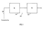
- a digital-to-analog converter 100 adapted to convert an input digital signal to an analog output signal.
- the converter includes an upper part 105 that is responsible for converting a first portion of the digital input word comprising the most significant bit (MSB) of the digital input word and a lower part 110 responsible for converting the remaining portion (i.e. the least significant bits LSBs) of the digital input word.
- the resistance of the upper part, R2 can be less than that of the resistance of the lower part, R1.
- the DAC of the present invention converts an input word to a single analog output corresponding to that input word.
- the input word can be considered as being divisible into two sub-words: a first sub-word containing the least significant bits (LSBs) of the input word and the second sub-word containing the most significant bits (MSBs) of the input word, each of the two sub-words being converted by a part of the DAC.
- the lower part not only provides the corresponding analog output voltage signal for the LSB of the input word but also may be used to tune the upper part.
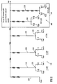
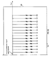
- the upper portion 105 includes a first set of segments 200, shown here as two segments 205, 210.
- the lower part is provided as three legs 215, 220, 225 in a traditional R-2R configuration, with each leg of the lower part providing 1, 2 or 4 LSBs contributing towards the output of the DAC.
- a termination leg 230 is coupled to Vref-, typically a ground signal.
- Each of the three legs of the lower part are switchably coupled via switches 235, 240, 245 respectively between Vref- and Vref+.
- the effect of switching each segment of the set of the upper part on the output of the DAC corresponds to the effect of switching multiples of one bit from the lower part of the digital input word (which is equivalent to a weighting less than one LSB of the upper part of the word)
- the first segment is provided with a weighting of 8/3 LSBs and the second a weighting of 16/3 LSBs (being equivalent to 1 /3 and 2/3 the nominal weight of the bit of the upper part of the word).
- the effect is equal to 8 LSB as in a standard R- 2R arrangement.
- the code loaded to the LSB section of the DAC can be modified to correct the output, i.e. load 10001 for code 7 instead of code 10010 to correct for an error of +1 LSB DNL.
- This basic scheme can be extended to calibrate high resolution DACs.
- the legs of the lower part of the DAC are used to tune the output of the DAC when a segment from the set of the upper part has been selected.
- the calibration algorithm that is used is such to ensure that the lower part is never implemented in full deflection, -i.e. that the legs of the lower part are either all on or all off.
- the legs of the lower part may be used to tune or adapt the contribution from the segments of the upper part to provide the desired output from the DAC for the input digital word, and preferably can be used to ensure that there is no deviation from +DNL ⁇ 1 LSB
- the lower part is preferably provided in a ladder configuration.
- the present invention also provides for modifications to such conventional ladder configurations.
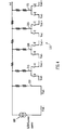
- a modification of a standard R-2R structure shown in Figure 3 , some of the link 'R' resistors, between adjacent legs, are removed and the remaining DAC resistors scaled, i.e. those resistors provided on the legs of the ladder between the termination leg and the removed resistor.
- the number of resistors is increased twofold so that there is provided a 2R-4R configuration.
- the lower part of the DAC is preferably provided with a termination leg, the termination leg being directly coupled to a reference signal, typically ground. It is also known to couple the termination leg of such ladder configurations to ground via a switch, but in accordance with preferred embodiments of the present invention, the coupling is direct as opposed to via the switch.
- a modification to a ladder configuration is provided where in the ladder is additionally coupled to a current source 400, the current source being configured to inject a scaled current (related to the reference) into a node of the R- 2R ladder.
- a scaled current (related to the reference) into a node of the R- 2R ladder.
- Such an injection may be added to any node of the ladder but typically is coupled to the top of a termination resistor, as is shown in Figure 4 . It is preferable to couple the current source to the termination leg as the available headroom within the DAC architecture is greatest here and as such it is easier to design the current source.
- R-2R DAC ladder architecture enables one to extend the resolution of the R-2R DAC without increasing the number of resistors and switches. This serves to extend the resolution provided by such architectures. It will be appreciated that the value of the current injected into the termination leg is typically of the order of microamps, whereas if the current was injected into other legs of the ladder, a signal of much reduced magnitudes would typically be required.
- FIG. 5 shows an example of the type of current source circuit that may be used in implementations of DACs according to the present invention. It will be appreciated however that the structure and components illustrated are exemplary of the type of configuration that may be considered by a person skilled in the art to provide a current injection to the resistor ladder of Figure 4 .
- an amplifier A is provided whose non-inverting input is coupled to Vref+.
- the inverting input is coupled in a feedback configuration to a resistor and a switch Q2, the values of which are scaled to the values of the switches and resistors in the legs of the lower part of the DAC.
- the gate of the switch Q2 is controlled by a bias voltage Vbias, so as to achieve the scaling effect.
- the output of the amplifier controls the gate of a second switch Q1, the source of which controls a master MOSFET device of a mirror arrangement.
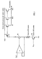
- the mirror is adapted to provide for the selective coupling of currents- shown here as B0, B0/2 and B0/4 into the termination leg of the lower part of the DAC- not shown in this Figure, but were previously shown in Figure 3 .
- the selective switching achieves the injection of current equivalent of 1 LSB, 1 LSB/2 and 1 LSB/4 respectively.
- Such injection of current is advantageous in that it improves the resolution of the DAC without requiring additional legs within the resistor ladder DAC arrangement.
- any one of the three embodiments may be used independently of the others, but in preferred implementations all three are combined.
- Such an example is shown in the architecture of Figure 6 .
- Figure 6 has been subdivided into three sheets shown as Figures 6A , 6B and 6C . These can be read in conjunction with one another to view the entire DAC structure.
- the upper part 105 is adapted to provide 4 bits of the input word.
- the lower part of the DAC is provided as a modified R-2R architecture with the link resistor between the lower part and the upper part removed, such that the lower legs (legs B1-B11), (i.e. those legs below the region where the link resistor traditionally would have been found), scaled to provide a 2R-4R architecture.
- the four bits after the segments B11, B10, B9, B8 are alternatively split into the nominal weighting sets of Figure 2 , shown here as 1/3 and 2/3 nominal weighting arrangements.
- the following seven bits (B7...B1) are provided as a standard 2R-4R implementation.
- Bit 0 and weights of LSB/2 and LSB/4 are generated by coupling the termination leg to a current source and using the current source to inject currents into the mid point of that leg, i.e. in the mid point of the 4 resistors provided the termination leg.
- the weights less than 1 LSB are adapted to give extra resolution to the DAC if so required.
- each of the legs (B0-B11 and S0-S14) are switchably coupled to a voltage reference, as is normal for resistor ladder configurations, but for the sake of convenience the individual switch components are not shown.
- the teaching herein provides for an improved DAC architecture where the improvements may be provided independently or in combination with one another.
- This teaching is specifically adapted to provide a DAC structure optimized for digital calibration. The goal is achieved this by providing a DAC structure comprising an upper part defining a main part of the DAC architecture and a lower part defining a subDAC part of the architecture.
- the subDAC part is used to provide a tuning of the upper part of the DAC so as to ensure that for increasing input code applied to the DAC, the DAC provides an output which does not vary by more than 1 LSB. This is achieved by selective switching of the upper and lower parts of the DAC together.
- the underlying DAC architecture should have resolution greater than the desired resolution of the calibrated output and should also have a means of guaranteeing that there are no gaps in the transfer function (i.e., a means of ensuring no positive DNL errors > 1 LSB). These requirements are met by the architectures discussed herein.
- Figure 7 shows a schematic of a DAC calibration system 700 provided for practicing the invention.
- the system provides an apparatus & method for generating a linear, resistor ladder, voltage output DAC in the presence of component matching errors.
- a sixteen bit user input word is provided at a interface decode 705, where the MSBs and LSBs of the word are separated.
- the DAC 700 including a main-section 710 converting the MSBs of the DAC word into an output voltage and a sub-section 715 converting the LSBs of the DAC word.
- the sections are coupled together to provide an overall output voltage at an output 720.
- the main-section 710 may be provided in a configuration, such as that shown in Figure 6 as block 105, containing a resistor ladder structured so that it's LSB is less than full-scale of the sub-section 715 but substantially greater than both the LSB of the sub-section & the overall DAC transfer function LSB.
- the sub-section 715 also containing a resistor ladder structure, an example of the type of structure being shown as block 110 in Figure 6 .
- the ladder structures of the main-section is arranged and the sub-section is scaled so that (in the absence of mismatch) all voltage points in the DAC transfer function (except zero scale (ZS) and full scale (FS)) can be obtained without loading ZS or FS to the sub-section DAC. In this manner it will be apparent that the sub-section DAC uses a reduced code range.
- the interface decode is structured to select a main-section & sub-section DAC word for every user input code (except full scale) so that when a main-section code is selected the sub-section is not at zero-scale or full scale.
- a calibration memory 725 which stores error corrections for each segment of the main-section, is also provided. Selected corrections from the data stored in this memory may be added for each segment of the main-section selected to the LSB word using an adder 730.
- the error in the segments of the main section is measured and corresponding corrections stored in the memory 725. These corrections are then automatically added to the code loaded to the sub-section depending on the main-section code loaded (i.e. the segments selected in the ladder of the main section).
- the present invention provides a DAC configuration that can be used to convert a digital input word into an analog voltage output.
- the illustrated embodiments and principles of operation have been described with reference to an upper and a lower part or a first and second component but it will be appreciated that such nomenclature is used for ease of explanation and it is not intended to limit the protection in any way except as may be deemed necessary in the light of the appended claims. Similarly modifications can be made and will be apparent to those skilled in the art to the exemplary embodiments described herein without departing from the spirit and scope of the present invention.
Description
- The present invention relates to digital-to-analog converters (DACs) and in particular to DAC structures implemented using resistive ladder configurations. The invention more particularly relates to DAC structures based on an R-2R configuration.
- DAC structures are well known in the art. They are used to convert an input digital signal, usually provided in the form of a binary code, to an analog output signal- either in the form of a corresponding voltage or current. This is achieved using switches or a network of resistors or current sources.
- An example of known DAC structures is given in
US Patent 5 764 174 (USP '174) of Dempsey et al which is assigned to the Assignee of the present application, the content of which is incorporated herein by reference. USP '174 describes an R-2R ladder structure which includes a plurality of legs. Each leg contributes towards the resolution of the device, such that the more legs that are provided in the structure the better the resolution. However, as one adds more legs to the ladder structure it is also necessary to add a plurality of corresponding switches, which need to be scaled appropriately. The addition of switches is not a trivial activity, as each new switch needs to be scaled appropriately to the preceding switch. This scaling of the switches is addressed by the invention of USP'174 which provides a control circuit such that the on resistance of the switches is controlled with regard to a reference value. However, if one wants high resolution from the DAC there is still the problem of keeping the switches in reasonable operating parameters and in providing sufficient area on the circuit layout to accommodate for the large number of switches. - A further issue with high resolution DACs is that the linearity and monotonicity of the DAC is limited by component matching. Random component mismatch can reduce the monotonicity and linearity of the DAC structure. This problem has traditionally been countered either by laser trimming components to adjust their values or by incorporating calibration circuitry on board.
-
JP2001 127634 -
JP11017547 - Schoeff John A (" An inherent Monotonic 12-Bit DAC" IEE Journal of Solid-State Circuits, Vol. SC-14, December 1979 (1979-12) pages 904-911, XP00235323 presents a 12bit DAC which uses diffused resistors and requires no trimming to guarantee monoticity for all grades over the temperature range. The DAC comprises an R2R ladder which departs from the traditional R2R approach.
- Greenly B R et al ("A 1.4V 10b CMOS DC DAC in 0.01 mm<2> "SOC Conference, 2003. Proceedings. IEEE International [Systems-On-Chip] 17-20 SEPT. 2003, Piscataway, NJ, USA, IEEE, 17 September 2003 (2003-09-17), pages 237-238, XP10665618 ISBN: 0-7803-8182-3 presents a laser trimming technique and an application to improve the linearity of a 10bit DAC.
- There is therefore a need to provide a DAC configuration which is adopted to provide for high DAC resolution and which facilitates calibration of DAC linearity errors.
- Accordingly, a first embodiment of the invention provides a digital-to-analog converter as detailed in
claim 1. The invention also provides a method as detailed in claim 17. Advantageous embodiments are provided in the dependent claims. - The ladder may typically be provided in a R-2R topology or modified version thereto. In such a modification of the standard R- 2R structure some of the link 'R' resistors are removed and the remaining DAC resistors scaled. This increases the impedance of the first component or lower DAC section at the expense of resistor area but reduces the current flowing in the DAC and also reduces the effect of switch and wiring non-idealities relative to the resistor value in the lower part of the DAC.
- By coupling a lower part of the DAC to a current source, the current source being configured to inject a scaled current (related to the reference) into a node of the R- 2R ladder the present invention provides for a minimization of the total DAC area for a given resolution and reduces the switch scaling problem. Such an injection may be added to any node of the ladder but typically is coupled to the top of a termination resistor.
- These and other features of the present invention will be better understood with reference to the drawings that follow.
- The present invention will now be described with reference to the accompanying drawings in which:
-
Figure 1 is a schematic of a DAC configuration according to a first illustrative embodiment for practicing the invention; -
Figure 2 is an example of a 4-bit DAC architecture according to the embodiment ofFigure 1 ; -
Figure 3 is an example of a DAC architecture in accordance with an illustrative second embodiment;. -
Figure 4 is an example of a DAC architecture in accordance with a third embodiment;. -
Figure 5 is an example of a current source that may be used with the embodiment ofFigure 4 ; -
Figures 6A ,6B and6C are schematic of a DAC architecture incorporating all three embodiments illustrated inFigures 2 ,3 and4 ; and -
Figure 7 is a schematic showing an illustrative fourth embodiment. - The present invention will now be described with reference to
Figures 1 to 6 . As shown inFigure 1 , in accordance with a first illustrative embodiment of a DAC practicing the present invention, a digital-to-analog converter 100 adapted to convert an input digital signal to an analog output signal is provided. The converter includes anupper part 105 that is responsible for converting a first portion of the digital input word comprising the most significant bit (MSB) of the digital input word and alower part 110 responsible for converting the remaining portion (i.e. the least significant bits LSBs) of the digital input word. The resistance of the upper part, R2, can be less than that of the resistance of the lower part, R1. It will be understood that the DAC of the present invention converts an input word to a single analog output corresponding to that input word. For the sake of explanation, however, the input word can be considered as being divisible into two sub-words: a first sub-word containing the least significant bits (LSBs) of the input word and the second sub-word containing the most significant bits (MSBs) of the input word, each of the two sub-words being converted by a part of the DAC. In accordance with the present invention, the lower part not only provides the corresponding analog output voltage signal for the LSB of the input word but also may be used to tune the upper part. - As shown in
Figure 2 , which it will be appreciated is an exemplary embodiment of the configuration ofFigure 1 as implemented as a 4-bit DAC, theupper portion 105 includes a first set ofsegments 200, shown here as twosegments legs termination leg 230 is coupled to Vref-, typically a ground signal. Each of the three legs of the lower part are switchably coupled viaswitches - The effect of switching each segment of the set of the upper part on the output of the DAC corresponds to the effect of switching multiples of one bit from the lower part of the digital input word (which is equivalent to a weighting less than one LSB of the upper part of the word) In the example of
Figure 2 for a 4-bit DAC, the first segment is provided with a weighting of 8/3 LSBs and the second a weighting of 16/3 LSBs (being equivalent to 1 /3 and 2/3 the nominal weight of the bit of the upper part of the word). When both of the segments of the upper part are switched together, the effect is equal to 8 LSB as in a standard R- 2R arrangement. But these elements can also be switched independently giving the effect on the output of 8/3 LSBs and 16/3 LSBs . As such this set of segments can be thought of as providing a switched resistance whose effect on the DAC output straddles the effect of the preceding leg. Taking account of the matching of the resistors (which will be known for each process), the DAC structure ofFigure 2 can be modified to guarantee that internally within the DAC there is a switch combination which be will approximate all the desired output voltages. The calibration algorithm then becomes a technique of mapping input codes to the switch code which gives the desired output. -
Figure 2 also indicates the bit weight of each switchable element. This is the effect on the DAC output when each bit is switched. As expected for a 4-bit DAC, the output when all elements are switched is equal to 15 LSBs. Table 1 below shows two possible switching sequences which equal or approximate the desired transfer function Output = Code <*> LSB. In the absence of resistor errors,sequence 1 gives the ideal output for each input code. In the presence of positive DNL errors at the midscale transition from code 7 to code 8 (8/ 3 or 16/3 weight or both weights too big) then this DAC cannot be corrected if switchingsequence 1 is used. If the second sequence is selected then, in the absence of mismatch it approximates the ideal output for each input code. In the presence of a positive DNL error due to either the 8/ 3 or 16/ 3 segment or both being too big, the code loaded to the LSB section of the DAC can be modified to correct the output, i.e. load 10001 for code 7 instead of code 10010 to correct for an error of +1 LSB DNL. This basic scheme can be extended to calibrate high resolution DACs.Table 1 Input Code Option 1 switching sequence Option 2 switching sequence 0 00000 00000 = 0 1 00001 00001 = 1 2 00010 00010 = 2 3 00011 00011 = 3 4 00100 00100 = 4 5 00101 00101 = 5 6 00110 00110 = 6 7 00111 10010 = 7.333 8 11000 10011 = 8.333 9 11001 10100 = 9.333 10 11010 10101 = 10.333 11 11011 11011 = 11 12 11100 11100 = 12 13 11101 11101 = 13 14 11110 11110 = 14 15 11111 11111 = 15 - It will be appreciated therefore that if the second switching sequence is used, that the legs of the lower part of the DAC are used to tune the output of the DAC when a segment from the set of the upper part has been selected. The calibration algorithm that is used is such to ensure that the lower part is never implemented in full deflection, -i.e. that the legs of the lower part are either all on or all off. As such, the legs of the lower part may be used to tune or adapt the contribution from the segments of the upper part to provide the desired output from the DAC for the input digital word, and preferably can be used to ensure that there is no deviation from +DNL<1 LSB
- The use of a configuration such as that shown in
Figure 2 is advantageous in applications where there is a requirement for digital calibration to have a positive DNL < 1 LSB. This is difficult to guarantee in a high resolution standard R- 2R structure due to resistor matching limitations. If the midscale transition from 0111 to 1000 in a standard 4-bit R- 2R DAC has a positive DNL > 1 LSB, then there is a desired output voltage which cannot be obtained no matter what code is loaded to the DAC. In the example ofFigure 2 , the R-2R structure has been modified to add redundancy. In a standard N bit R-2R structure there are N switchable elements giving 2N possible outputs. In accordance with the present invention, there are N+ X switchable elements giving 2(N+X) possible outputs. These additional switchable elements are structured and sequenced in such a way as to guarantee that positive DNL < 1 LSB. - As shown in
Figure 2 , the lower part is preferably provided in a ladder configuration. The present invention also provides for modifications to such conventional ladder configurations. In such a modification of a standard R-2R structure, shown inFigure 3 , some of the link 'R' resistors, between adjacent legs, are removed and the remaining DAC resistors scaled, i.e. those resistors provided on the legs of the ladder between the termination leg and the removed resistor. In this instance, the number of resistors is increased twofold so that there is provided a 2R-4R configuration. This increases the impedance of these lower legs at the expense of resistor area but reduces the current flowing in the DAC and also reduces the effect of switch and wiring non-idealities relative to the resistor value in these lower legs of the DAC. By doubling the values of the resistors, most of the voltage in the legs is dropped across the resistors as opposed to the switches. As a result the contribution of the resistance of the switches to the legs is less, and their associated scaling problem contributes less in error than heretofore achievable. - As has been described heretofore, the lower part of the DAC is preferably provided with a termination leg, the termination leg being directly coupled to a reference signal, typically ground. It is also known to couple the termination leg of such ladder configurations to ground via a switch, but in accordance with preferred embodiments of the present invention, the coupling is direct as opposed to via the switch.
- In accordance with a third embodiment, a modification to a ladder configuration is provided where in the ladder is additionally coupled to a
current source 400, the current source being configured to inject a scaled current (related to the reference) into a node of the R- 2R ladder. This minimizes total DAC area for a given resolution and reduces the switch scaling problem. Such an injection may be added to any node of the ladder but typically is coupled to the top of a termination resistor, as is shown inFigure 4 . It is preferable to couple the current source to the termination leg as the available headroom within the DAC architecture is greatest here and as such it is easier to design the current source. The combination of an R-2R DAC ladder architecture and the current source DAC enables one to extend the resolution of the R-2R DAC without increasing the number of resistors and switches. This serves to extend the resolution provided by such architectures. It will be appreciated that the value of the current injected into the termination leg is typically of the order of microamps, whereas if the current was injected into other legs of the ladder, a signal of much reduced magnitudes would typically be required. -
Figure 5 shows an example of the type of current source circuit that may be used in implementations of DACs according to the present invention. It will be appreciated however that the structure and components illustrated are exemplary of the type of configuration that may be considered by a person skilled in the art to provide a current injection to the resistor ladder ofFigure 4 . In this example, an amplifier A is provided whose non-inverting input is coupled to Vref+. The inverting input is coupled in a feedback configuration to a resistor and a switch Q2, the values of which are scaled to the values of the switches and resistors in the legs of the lower part of the DAC. The gate of the switch Q2 is controlled by a bias voltage Vbias, so as to achieve the scaling effect. The output of the amplifier controls the gate of a second switch Q1, the source of which controls a master MOSFET device of a mirror arrangement. The mirror is adapted to provide for the selective coupling of currents- shown here as B0, B0/2 and B0/4 into the termination leg of the lower part of the DAC- not shown in this Figure, but were previously shown inFigure 3 . The selective switching achieves the injection of current equivalent of 1 LSB, 1 LSB/2 and 1 LSB/4 respectively. Such injection of current is advantageous in that it improves the resolution of the DAC without requiring additional legs within the resistor ladder DAC arrangement. - It will be understood that any one of the three embodiments , for example those shown in
Figures 2 ,3 and4 , may be used independently of the others, but in preferred implementations all three are combined. Such an example is shown in the architecture ofFigure 6 . For the sake of clarity,Figure 6 has been subdivided into three sheets shown asFigures 6A ,6B and6C . These can be read in conjunction with one another to view the entire DAC structure. In this embodiment ofFigure 6 , theupper part 105 is adapted to provide 4 bits of the input word. These four bits are provided in a segmented architecture with fifteen equal-weighted segments, 14 legs S1 to S14 each having two resistors and one leg/segments (S0)being further divided to provide a set having a first segment of 1/3 nominal weight and thesecond segment 2/3 the nominal weight. This is provided by 6 resistors in the first leg (Leg S0A) and 3 resistors in the second leg (Leg SOB). - The lower part of the DAC is provided as a modified R-2R architecture with the link resistor between the lower part and the upper part removed, such that the lower legs (legs B1-B11), (i.e. those legs below the region where the link resistor traditionally would have been found), scaled to provide a 2R-4R architecture. The four bits after the segments B11, B10, B9, B8 are alternatively split into the nominal weighting sets of
Figure 2 , shown here as 1/3 and 2/3 nominal weighting arrangements. The following seven bits (B7...B1) are provided as a standard 2R-4R implementation. Bit 0 and weights of LSB/2 and LSB/4 are generated by coupling the termination leg to a current source and using the current source to inject currents into the mid point of that leg, i.e. in the mid point of the 4 resistors provided the termination leg. The weights less than 1 LSB are adapted to give extra resolution to the DAC if so required. As an example of the type of current that should be injected into the termination leg to give the desired results, this current source should inject
(where swres1 = resistance of switch on B1 leg) to give an output change of Lsb/4. - It will be understood that each of the legs (B0-B11 and S0-S14) are switchably coupled to a voltage reference, as is normal for resistor ladder configurations, but for the sake of convenience the individual switch components are not shown.
- It will be appreciated that the teaching herein provides for an improved DAC architecture where the improvements may be provided independently or in combination with one another. This teaching is specifically adapted to provide a DAC structure optimized for digital calibration. The goal is achieved this by providing a DAC structure comprising an upper part defining a main part of the DAC architecture and a lower part defining a subDAC part of the architecture. The subDAC part is used to provide a tuning of the upper part of the DAC so as to ensure that for increasing input code applied to the DAC, the DAC provides an output which does not vary by more than 1 LSB. This is achieved by selective switching of the upper and lower parts of the DAC together.
- In order to calibrate the DNL & INL errors of a DAC using a digital calibration algorithm the underlying DAC architecture should have resolution greater than the desired resolution of the calibrated output and should also have a means of guaranteeing that there are no gaps in the transfer function (i.e., a means of ensuring no positive DNL errors > 1 LSB). These requirements are met by the architectures discussed herein.
-
Figure 7 shows a schematic of aDAC calibration system 700 provided for practicing the invention. The system provides an apparatus & method for generating a linear, resistor ladder, voltage output DAC in the presence of component matching errors. In this illustrative example a sixteen bit user input word is provided at ainterface decode 705, where the MSBs and LSBs of the word are separated. - The
DAC 700 including a main-section 710 converting the MSBs of the DAC word into an output voltage and asub-section 715 converting the LSBs of the DAC word. The sections are coupled together to provide an overall output voltage at anoutput 720. - The main-
section 710 may be provided in a configuration, such as that shown inFigure 6 asblock 105, containing a resistor ladder structured so that it's LSB is less than full-scale of thesub-section 715 but substantially greater than both the LSB of the sub-section & the overall DAC transfer function LSB. - The
sub-section 715 also containing a resistor ladder structure, an example of the type of structure being shown asblock 110 inFigure 6 . - It will be understood that the ladder structures of the main-section is arranged and the sub-section is scaled so that (in the absence of mismatch) all voltage points in the DAC transfer function (except zero scale (ZS) and full scale (FS)) can be obtained without loading ZS or FS to the sub-section DAC. In this manner it will be apparent that the sub-section DAC uses a reduced code range.
- The interface decode is structured to select a main-section & sub-section DAC word for every user input code (except full scale) so that when a main-section code is selected the sub-section is not at zero-scale or full scale. A
calibration memory 725, which stores error corrections for each segment of the main-section, is also provided. Selected corrections from the data stored in this memory may be added for each segment of the main-section selected to the LSB word using anadder 730. - During production tests, the error in the segments of the main section is measured and corresponding corrections stored in the
memory 725. These corrections are then automatically added to the code loaded to the sub-section depending on the main-section code loaded (i.e. the segments selected in the ladder of the main section). - As will be understood by those skilled in the art, the present invention provides a DAC configuration that can be used to convert a digital input word into an analog voltage output. The illustrated embodiments and principles of operation have been described with reference to an upper and a lower part or a first and second component but it will be appreciated that such nomenclature is used for ease of explanation and it is not intended to limit the protection in any way except as may be deemed necessary in the light of the appended claims. Similarly modifications can be made and will be apparent to those skilled in the art to the exemplary embodiments described herein without departing from the spirit and scope of the present invention.
- The words "comprise", "comprises", and "comprising" when used in this specification are to specify the presence of stated features, integers, steps or components but does not preclude the presence or addition of one or more other features, integers, steps, components or groups thereof.
Claims (17)
- A digital-to-analog converter (DAC) adapted to convert a digital input word to an analog output voltage signal, the digital input word being divisible into an upper part and a lower part, the DAC including: a first resistor ladder DAC controlled by the lower part of the word and generating an output voltage, and a second resistor ladder DAC controlled by the upper part of the word and generating an output voltage, the first resistor ladder DAC comprises plurality of binary weighted branches, the second resistor ladder DAC comprises at least two discrete segments, each discrete segment having a weighting corresponding to multiples of one bit of the lower part of the word and the at least two discrete segments amounting to the nominal weight of the corresponding bit of the upper part of the word, characterised in that: a switching sequence derived from a calibration phase controls the branches of the first resistor ladder DAC and the segments of the second resistor ladder DAC such that the output voltage of the DAC results in a desired value, wherein said switching sequence is different from the switching sequence of the original digital input word and ensures that the lower part of the word is never implemented in full deflection.
- The DAC as claimed in claim 1 wherein the weighting of at least one of the segments of the second resistor ladder DAC is less than the total weighting of the lower part of the word.
- The DAC as claimed in claim 1 wherein the ladder of the first resistor ladder DAC has an R-2R architecture.
- The DAC as claimed in claim 3 wherein the ladder of the first resistor ladder DAC has a scaled R-2R architecture, comprising legs having a plurality of resistors, the legs being separated by link resistors.
- The DAC as claimed in claim 4 wherein at least one of the link resistors is removed as compared with a conventional R-2R architecture and the remaining leg resistors are scaled consistent with that removal.
- The DAC as claimed in claim 1 wherein the first resistor ladder DAC is provided with a termination leg, the termination leg being directly coupled to reference signal.
- The DAC as claimed in claim 1 wherein the first resistor ladder DAC is coupled to a current source, the current source being configured to inject a scaled current into a node of the ladder.
- The DAC as claimed in claim 7 wherein the injected current is injected to a termination leg of the ladder.
- A DAC as claimed in claim 6 wherein the termination leg is coupled to a reference voltage and a plurality of switchable legs are provided each being switchably coupled to a reference voltage, and wherein at least one of the individual segments is additionally coupled to a current source, the current source being adapted to inject an adjustable current into the first resistor ladder DAC so as to increase the resolution of the DAC.
- The DAC as claimed in claim 9 wherein the current injected into the first resistor ladder DAC is scaled relative to the reference voltage.
- The DAC as claimed in claim 9 wherein the value of the resistance being provided in the legs of the first resistor ladder DAC being twice the value of the resistance in the legs of the second resistor ladder DAC.
- The DAC as claimed in claim 11 wherein an upper leg of the first resistor ladder DAC is directly coupled to a lower leg of the second resistor ladder DAC without a coupling resistor, such that the resistance of the legs in the first resistor ladder DAC is a scaled multiple of the resistance of the legs in the second portion.
- The DAC as claimed in claim 12 wherein at least one leg is segmented.
- A DAC as claimed in claim 1 wherein an interface decode structured to select the first resistor ladder DAC and the second resistor ladder DAC word for input user codes such that when a second resistor ladder DAC code is selected the first resistor ladder DAC is between zero and full scale, the interface decode separating the input digital code to an MSB DAC word and an LSB DAC word; a calibration memory for storing DNL and/or INL error corrections for the second resistor ladder DAC, and an adder for adding selected error correction from the calibration memory to the LSB DAC word.
- The DAC of claim 14 wherein the calibration memory is loaded with error corrections during a production test of the DAC.
- The DAC of claim 14 wherein the adder is configured to automatically add the corrections to the code loaded to the first resistor ladder DAC on selection of a predetermined segment of the second resistor ladder DAC.
- A method of converting a digital input word to a corresponding output voltage, the method including the steps of: dividing the digital input word into a lower part and an upper part, converting the lower part of the digital input word to a corresponding voltage output using a first resistor ladder digital to analog converter (DAC), converting the upper part of the digital input word to a corresponding voltage output using a second resistor ladder digital to analog converter, the first resistor ladder DAC comprises plurality of binary weighted branches, the second resistor ladder DAC comprises at least two discrete segments, each discrete segment having a weighting corresponding to multiples of one bit of the lower part of the word and the at least two discrete segments amounting to the nominal weight of the corresponding bit of the upper part of the word, characterised in that: a switching sequence derived from a calibration phase controls the branches of the first resistor ladder DAC and the segments of the second resistor ladder DAC such that the output voltage of the DAC results in a desired value, wherein said switching sequence is different from the switching sequence of the original digital input word and ensures that the lower part of the word is never implemented in full deflection.
Applications Claiming Priority (3)
| Application Number | Priority Date | Filing Date | Title |
|---|---|---|---|
| US61146904P | 2004-09-20 | 2004-09-20 | |
| US11/048,374 US7095351B2 (en) | 2004-09-20 | 2005-02-01 | Digital-to-analog converter structures |
| PCT/EP2005/054141 WO2006032592A1 (en) | 2004-09-20 | 2005-08-23 | Digital-to-analog converter structures |
Publications (2)
| Publication Number | Publication Date |
|---|---|
| EP1792402A1 EP1792402A1 (en) | 2007-06-06 |
| EP1792402B1 true EP1792402B1 (en) | 2009-07-15 |
Family
ID=35159837
Family Applications (1)
| Application Number | Title | Priority Date | Filing Date |
|---|---|---|---|
| EP05774067A Not-in-force EP1792402B1 (en) | 2004-09-20 | 2005-08-23 | Digital-to-analog converter structures |
Country Status (7)
| Country | Link |
|---|---|
| US (1) | US7095351B2 (en) |
| EP (1) | EP1792402B1 (en) |
| JP (1) | JP4550901B2 (en) |
| CN (1) | CN101023583B (en) |
| DE (1) | DE602005015464D1 (en) |
| TW (1) | TWI296880B (en) |
| WO (1) | WO2006032592A1 (en) |
Families Citing this family (22)
| Publication number | Priority date | Publication date | Assignee | Title |
|---|---|---|---|---|
| US7173552B1 (en) * | 2003-10-01 | 2007-02-06 | Analog Devices, Inc. | High accuracy segmented DAC |
| TWI330001B (en) * | 2006-08-15 | 2010-09-01 | Realtek Semiconductor Corp | Dynamic bias control circuit and related apparatus for digital-to-analog converter |
| US7688240B2 (en) * | 2008-05-02 | 2010-03-30 | Analog Devices, Inc. | Method and apparatus for calibrating an RDAC for end-to-end tolerance correction of output resistance |
| CN101345527B (en) * | 2008-07-09 | 2010-06-02 | 清华大学 | D/A converter based on CeRAM unit |
| DE102010016556A1 (en) * | 2009-04-24 | 2010-11-25 | Intersil Americas Inc., Milpitas | Digital-to-analog-converter, has memory for storing digital information representing control voltages, and auxiliary-digital-analog-converter receiving information from memory and generating voltages for voltage sources |
| US8164495B2 (en) * | 2009-11-12 | 2012-04-24 | Intersil Americas Inc. | Integrated non-linearity (INL) and differential non-linearity (DNL) correction techniques for digital-to-analog converters (DACS) |
| CN101834605B (en) * | 2010-04-12 | 2013-03-06 | 智原科技股份有限公司 | System and method for testing analog-digital converter |
| CN101924554B (en) * | 2010-06-30 | 2013-07-03 | 中国电子科技集团公司第五十八研究所 | Common mode error calibrating circuit of charge coupled pipeline analog-to-digital converter (ADC) |
| US8514112B2 (en) | 2010-07-15 | 2013-08-20 | Analog Devices, Inc. | Programmable linearity correction circuit for digital-to-analog converter |
| JP6043052B2 (en) * | 2011-06-20 | 2016-12-14 | ティアック株式会社 | DA converter |
| CN102545906B (en) * | 2012-02-10 | 2015-01-07 | 英特格灵芯片(天津)有限公司 | Current digital to analog conversion method and device |
| US8537043B1 (en) * | 2012-04-12 | 2013-09-17 | Analog Devices, Inc. | Digital-to-analog converter with controlled gate voltages |
| US8576101B1 (en) | 2012-11-05 | 2013-11-05 | Google Inc. | Calibration of an R2R ladder based current digital-to-analog converter (DAC) |
| US8912939B2 (en) * | 2012-12-14 | 2014-12-16 | Analog Devices Technology | String DAC leakage current cancellation |
| CN103795415A (en) * | 2014-01-24 | 2014-05-14 | 中国人民解放军国防科学技术大学 | High-precision analog to digital conversion method and device based on double-path combination analog to digital converter |
| CN104168026B (en) * | 2014-08-25 | 2017-09-15 | 长沙瑞达星微电子有限公司 | A kind of segmented current steering DAC circuit |
| US9276598B1 (en) * | 2015-05-22 | 2016-03-01 | Texas Instruments Incorporated | Trim-matched segmented digital-to-analog converter apparatus, systems and methods |
| US10425098B2 (en) | 2017-05-04 | 2019-09-24 | Analog Devices Global | Digital-to-analog converter (DAC) termination |
| WO2018232614A1 (en) * | 2017-06-21 | 2018-12-27 | Texas Instruments Incorporated | Segmented digital-to-analog converter |
| WO2021133708A1 (en) * | 2019-12-23 | 2021-07-01 | Texas Instruments Incorporated | Hybrid multiplying digital analog converter |
| CN113517891B (en) * | 2021-09-13 | 2022-01-04 | 成都爱旗科技有限公司 | Linear calibration system and method applied to digital-to-analog converter |
| CN115694483B (en) * | 2022-10-17 | 2024-03-29 | 电子科技大学 | Resistor network, low-temperature digital-to-analog converter circuit, chip and related devices |
Family Cites Families (6)
| Publication number | Priority date | Publication date | Assignee | Title |
|---|---|---|---|---|
| US5119094A (en) * | 1989-11-20 | 1992-06-02 | Analog Devices, Inc. | Termination circuit for an r-2r, ladder that compensates for the temperature drift caused by different current densities along the ladder, using one type of biopolar transistor |
| US5764174A (en) | 1996-05-14 | 1998-06-09 | Analog Devices, Inc. | Switch architecture for R/2R digital to analog converters |
| JPH1117547A (en) | 1997-06-19 | 1999-01-22 | Sanyo Electric Co Ltd | Digital-to-analog converter |
| JP4311511B2 (en) * | 1999-10-25 | 2009-08-12 | 日本バーブラウン株式会社 | Method and apparatus for digital-analog conversion |
| JP3803900B2 (en) | 1999-11-01 | 2006-08-02 | ローム株式会社 | Digital / analog converter |
| US6429798B1 (en) * | 2000-02-08 | 2002-08-06 | Ericsson Inc. | Combined transmit filter and D-to-A converter |
-
2005
- 2005-02-01 US US11/048,374 patent/US7095351B2/en active Active
- 2005-08-23 WO PCT/EP2005/054141 patent/WO2006032592A1/en active Application Filing
- 2005-08-23 DE DE602005015464T patent/DE602005015464D1/en active Active
- 2005-08-23 EP EP05774067A patent/EP1792402B1/en not_active Not-in-force
- 2005-08-23 CN CN2005800312534A patent/CN101023583B/en not_active Expired - Fee Related
- 2005-08-23 JP JP2007531737A patent/JP4550901B2/en not_active Expired - Fee Related
- 2005-09-20 TW TW094132559A patent/TWI296880B/en not_active IP Right Cessation
Also Published As
| Publication number | Publication date |
|---|---|
| JP4550901B2 (en) | 2010-09-22 |
| WO2006032592A1 (en) | 2006-03-30 |
| JP2008514065A (en) | 2008-05-01 |
| EP1792402A1 (en) | 2007-06-06 |
| DE602005015464D1 (en) | 2009-08-27 |
| CN101023583B (en) | 2012-10-10 |
| TWI296880B (en) | 2008-05-11 |
| TW200637160A (en) | 2006-10-16 |
| US20060061500A1 (en) | 2006-03-23 |
| CN101023583A (en) | 2007-08-22 |
| US7095351B2 (en) | 2006-08-22 |
Similar Documents
| Publication | Publication Date | Title |
|---|---|---|
| EP1792402B1 (en) | Digital-to-analog converter structures | |
| EP1510009B1 (en) | Method for calibrating a digital-to-analog converter and a digital-to-analog converter | |
| US7068201B1 (en) | Digital-to-analog converter | |
| US6329941B1 (en) | Digital-to-analog converting device and method | |
| US7978110B2 (en) | Digital-to-analog converter | |
| US6703956B1 (en) | Technique for improved linearity of high-precision, low-current digital-to-analog converters | |
| US20050001747A1 (en) | All-analog calibration of string-DAC linearity: application to high voltage processes | |
| EP1869770B1 (en) | Improved network adjustment circuits and methodologies | |
| US6509857B1 (en) | Digital-to-analog converting method and digital-to-analog converter | |
| EP2487797A1 (en) | Minimum differential non-linearity trim DAC | |
| EP3624345B1 (en) | Digital-to-analog converter transfer function modification | |
| JP4671766B2 (en) | Digital-analog converter and digital-analog conversion method | |
| WO2006103673A2 (en) | A low-power inverted ladder digital-to-analog converter | |
| US4523182A (en) | PROM trimmed digital-to-analog converter | |
| US7173552B1 (en) | High accuracy segmented DAC | |
| US6642867B1 (en) | Replica compensated heterogeneous DACs and methods | |
| CN112152622A (en) | Digital-to-analog converter | |
| US6995701B1 (en) | Multichannel high resolution segmented resistor string digital-to-analog converters | |
| US7633415B2 (en) | System and method for calibrating digital-to-analog convertors | |
| US7046182B1 (en) | DAC having switchable current sources and resistor string | |
| KR100335864B1 (en) | Digital/analog converter and digital/analog converting method | |
| CN114785350A (en) | Linear DAC modified by input code | |
| US6879276B2 (en) | Split cell bowtie digital to analog converter and method | |
| Ikeda et al. | A 14-bit 100-MS/s digitally calibrated binary-weighted current-steering CMOS DAC without calibration ADC | |
| KR20000072961A (en) | Current segment type digital-analog converter |
Legal Events
| Date | Code | Title | Description |
|---|---|---|---|
| PUAI | Public reference made under article 153(3) epc to a published international application that has entered the european phase |
Free format text: ORIGINAL CODE: 0009012 |
|
| 17P | Request for examination filed |
Effective date: 20070315 |
|
| AK | Designated contracting states |
Kind code of ref document: A1 Designated state(s): AT BE BG CH CY CZ DE DK EE ES FI FR GB GR HU IE IS IT LI LT LU LV MC NL PL PT RO SE SI SK TR |
|
| 17Q | First examination report despatched |
Effective date: 20070921 |
|
| DAX | Request for extension of the european patent (deleted) | ||
| GRAP | Despatch of communication of intention to grant a patent |
Free format text: ORIGINAL CODE: EPIDOSNIGR1 |
|
| GRAS | Grant fee paid |
Free format text: ORIGINAL CODE: EPIDOSNIGR3 |
|
| GRAA | (expected) grant |
Free format text: ORIGINAL CODE: 0009210 |
|
| AK | Designated contracting states |
Kind code of ref document: B1 Designated state(s): AT BE BG CH CY CZ DE DK EE ES FI FR GB GR HU IE IS IT LI LT LU LV MC NL PL PT RO SE SI SK TR |
|
| REG | Reference to a national code |
Ref country code: CH Ref legal event code: EP Ref country code: GB Ref legal event code: FG4D |
|
| REG | Reference to a national code |
Ref country code: IE Ref legal event code: FG4D |
|
| REF | Corresponds to: |
Ref document number: 602005015464 Country of ref document: DE Date of ref document: 20090827 Kind code of ref document: P |
|
| NLV1 | Nl: lapsed or annulled due to failure to fulfill the requirements of art. 29p and 29m of the patents act | ||
| PG25 | Lapsed in a contracting state [announced via postgrant information from national office to epo] |
Ref country code: ES Free format text: LAPSE BECAUSE OF FAILURE TO SUBMIT A TRANSLATION OF THE DESCRIPTION OR TO PAY THE FEE WITHIN THE PRESCRIBED TIME-LIMIT Effective date: 20091026 Ref country code: AT Free format text: LAPSE BECAUSE OF FAILURE TO SUBMIT A TRANSLATION OF THE DESCRIPTION OR TO PAY THE FEE WITHIN THE PRESCRIBED TIME-LIMIT Effective date: 20090715 Ref country code: LT Free format text: LAPSE BECAUSE OF FAILURE TO SUBMIT A TRANSLATION OF THE DESCRIPTION OR TO PAY THE FEE WITHIN THE PRESCRIBED TIME-LIMIT Effective date: 20090715 Ref country code: IS Free format text: LAPSE BECAUSE OF FAILURE TO SUBMIT A TRANSLATION OF THE DESCRIPTION OR TO PAY THE FEE WITHIN THE PRESCRIBED TIME-LIMIT Effective date: 20091115 Ref country code: FI Free format text: LAPSE BECAUSE OF FAILURE TO SUBMIT A TRANSLATION OF THE DESCRIPTION OR TO PAY THE FEE WITHIN THE PRESCRIBED TIME-LIMIT Effective date: 20090715 Ref country code: SE Free format text: LAPSE BECAUSE OF FAILURE TO SUBMIT A TRANSLATION OF THE DESCRIPTION OR TO PAY THE FEE WITHIN THE PRESCRIBED TIME-LIMIT Effective date: 20090715 |
|
| PG25 | Lapsed in a contracting state [announced via postgrant information from national office to epo] |
Ref country code: LV Free format text: LAPSE BECAUSE OF FAILURE TO SUBMIT A TRANSLATION OF THE DESCRIPTION OR TO PAY THE FEE WITHIN THE PRESCRIBED TIME-LIMIT Effective date: 20090715 Ref country code: SI Free format text: LAPSE BECAUSE OF FAILURE TO SUBMIT A TRANSLATION OF THE DESCRIPTION OR TO PAY THE FEE WITHIN THE PRESCRIBED TIME-LIMIT Effective date: 20090715 Ref country code: NL Free format text: LAPSE BECAUSE OF FAILURE TO SUBMIT A TRANSLATION OF THE DESCRIPTION OR TO PAY THE FEE WITHIN THE PRESCRIBED TIME-LIMIT Effective date: 20090715 Ref country code: PL Free format text: LAPSE BECAUSE OF FAILURE TO SUBMIT A TRANSLATION OF THE DESCRIPTION OR TO PAY THE FEE WITHIN THE PRESCRIBED TIME-LIMIT Effective date: 20090715 |
|
| PG25 | Lapsed in a contracting state [announced via postgrant information from national office to epo] |
Ref country code: BG Free format text: LAPSE BECAUSE OF FAILURE TO SUBMIT A TRANSLATION OF THE DESCRIPTION OR TO PAY THE FEE WITHIN THE PRESCRIBED TIME-LIMIT Effective date: 20091015 Ref country code: MC Free format text: LAPSE BECAUSE OF NON-PAYMENT OF DUE FEES Effective date: 20090831 Ref country code: PT Free format text: LAPSE BECAUSE OF FAILURE TO SUBMIT A TRANSLATION OF THE DESCRIPTION OR TO PAY THE FEE WITHIN THE PRESCRIBED TIME-LIMIT Effective date: 20091115 |
|
| REG | Reference to a national code |
Ref country code: CH Ref legal event code: PL |
|
| PG25 | Lapsed in a contracting state [announced via postgrant information from national office to epo] |
Ref country code: LI Free format text: LAPSE BECAUSE OF NON-PAYMENT OF DUE FEES Effective date: 20090831 Ref country code: DK Free format text: LAPSE BECAUSE OF FAILURE TO SUBMIT A TRANSLATION OF THE DESCRIPTION OR TO PAY THE FEE WITHIN THE PRESCRIBED TIME-LIMIT Effective date: 20090715 Ref country code: CZ Free format text: LAPSE BECAUSE OF FAILURE TO SUBMIT A TRANSLATION OF THE DESCRIPTION OR TO PAY THE FEE WITHIN THE PRESCRIBED TIME-LIMIT Effective date: 20090715 Ref country code: EE Free format text: LAPSE BECAUSE OF FAILURE TO SUBMIT A TRANSLATION OF THE DESCRIPTION OR TO PAY THE FEE WITHIN THE PRESCRIBED TIME-LIMIT Effective date: 20090715 Ref country code: CH Free format text: LAPSE BECAUSE OF NON-PAYMENT OF DUE FEES Effective date: 20090831 Ref country code: RO Free format text: LAPSE BECAUSE OF FAILURE TO SUBMIT A TRANSLATION OF THE DESCRIPTION OR TO PAY THE FEE WITHIN THE PRESCRIBED TIME-LIMIT Effective date: 20090715 |
|
| PLBE | No opposition filed within time limit |
Free format text: ORIGINAL CODE: 0009261 |
|
| STAA | Information on the status of an ep patent application or granted ep patent |
Free format text: STATUS: NO OPPOSITION FILED WITHIN TIME LIMIT |
|
| PG25 | Lapsed in a contracting state [announced via postgrant information from national office to epo] |
Ref country code: BE Free format text: LAPSE BECAUSE OF FAILURE TO SUBMIT A TRANSLATION OF THE DESCRIPTION OR TO PAY THE FEE WITHIN THE PRESCRIBED TIME-LIMIT Effective date: 20090715 Ref country code: SK Free format text: LAPSE BECAUSE OF FAILURE TO SUBMIT A TRANSLATION OF THE DESCRIPTION OR TO PAY THE FEE WITHIN THE PRESCRIBED TIME-LIMIT Effective date: 20090715 |
|
| 26N | No opposition filed |
Effective date: 20100416 |
|
| PG25 | Lapsed in a contracting state [announced via postgrant information from national office to epo] |
Ref country code: IE Free format text: LAPSE BECAUSE OF NON-PAYMENT OF DUE FEES Effective date: 20090823 |
|
| PG25 | Lapsed in a contracting state [announced via postgrant information from national office to epo] |
Ref country code: GR Free format text: LAPSE BECAUSE OF FAILURE TO SUBMIT A TRANSLATION OF THE DESCRIPTION OR TO PAY THE FEE WITHIN THE PRESCRIBED TIME-LIMIT Effective date: 20091016 |
|
| PG25 | Lapsed in a contracting state [announced via postgrant information from national office to epo] |
Ref country code: IT Free format text: LAPSE BECAUSE OF FAILURE TO SUBMIT A TRANSLATION OF THE DESCRIPTION OR TO PAY THE FEE WITHIN THE PRESCRIBED TIME-LIMIT Effective date: 20090715 |
|
| PG25 | Lapsed in a contracting state [announced via postgrant information from national office to epo] |
Ref country code: LU Free format text: LAPSE BECAUSE OF NON-PAYMENT OF DUE FEES Effective date: 20090823 |
|
| PG25 | Lapsed in a contracting state [announced via postgrant information from national office to epo] |
Ref country code: HU Free format text: LAPSE BECAUSE OF FAILURE TO SUBMIT A TRANSLATION OF THE DESCRIPTION OR TO PAY THE FEE WITHIN THE PRESCRIBED TIME-LIMIT Effective date: 20100116 |
|
| PG25 | Lapsed in a contracting state [announced via postgrant information from national office to epo] |
Ref country code: TR Free format text: LAPSE BECAUSE OF FAILURE TO SUBMIT A TRANSLATION OF THE DESCRIPTION OR TO PAY THE FEE WITHIN THE PRESCRIBED TIME-LIMIT Effective date: 20090715 |
|
| PG25 | Lapsed in a contracting state [announced via postgrant information from national office to epo] |
Ref country code: CY Free format text: LAPSE BECAUSE OF FAILURE TO SUBMIT A TRANSLATION OF THE DESCRIPTION OR TO PAY THE FEE WITHIN THE PRESCRIBED TIME-LIMIT Effective date: 20090715 |
|
| REG | Reference to a national code |
Ref country code: FR Ref legal event code: PLFP Year of fee payment: 12 |
|
| REG | Reference to a national code |
Ref country code: FR Ref legal event code: PLFP Year of fee payment: 13 |
|
| REG | Reference to a national code |
Ref country code: FR Ref legal event code: PLFP Year of fee payment: 14 |
|
| PGFP | Annual fee paid to national office [announced via postgrant information from national office to epo] |
Ref country code: FR Payment date: 20210722 Year of fee payment: 17 |
|
| PGFP | Annual fee paid to national office [announced via postgrant information from national office to epo] |
Ref country code: GB Payment date: 20210720 Year of fee payment: 17 Ref country code: DE Payment date: 20210720 Year of fee payment: 17 |
|
| REG | Reference to a national code |
Ref country code: DE Ref legal event code: R119 Ref document number: 602005015464 Country of ref document: DE |
|
| GBPC | Gb: european patent ceased through non-payment of renewal fee |
Effective date: 20220823 |
|
| PG25 | Lapsed in a contracting state [announced via postgrant information from national office to epo] |
Ref country code: FR Free format text: LAPSE BECAUSE OF NON-PAYMENT OF DUE FEES Effective date: 20220831 Ref country code: DE Free format text: LAPSE BECAUSE OF NON-PAYMENT OF DUE FEES Effective date: 20230301 |
|
| PG25 | Lapsed in a contracting state [announced via postgrant information from national office to epo] |
Ref country code: GB Free format text: LAPSE BECAUSE OF NON-PAYMENT OF DUE FEES Effective date: 20220823 |