EP1784050A2 - Keramisches Heizelement und Verfahren zur Herstellung von keramischen Heizern. - Google Patents
Keramisches Heizelement und Verfahren zur Herstellung von keramischen Heizern. Download PDFInfo
- Publication number
- EP1784050A2 EP1784050A2 EP06255610A EP06255610A EP1784050A2 EP 1784050 A2 EP1784050 A2 EP 1784050A2 EP 06255610 A EP06255610 A EP 06255610A EP 06255610 A EP06255610 A EP 06255610A EP 1784050 A2 EP1784050 A2 EP 1784050A2
- Authority
- EP
- European Patent Office
- Prior art keywords
- plate member
- boron nitride
- conductive layer
- heater
- rod member
- Prior art date
- Legal status (The legal status is an assumption and is not a legal conclusion. Google has not performed a legal analysis and makes no representation as to the accuracy of the status listed.)
- Granted
Links
Images
Classifications
-
- H—ELECTRICITY
- H05—ELECTRIC TECHNIQUES NOT OTHERWISE PROVIDED FOR
- H05B—ELECTRIC HEATING; ELECTRIC LIGHT SOURCES NOT OTHERWISE PROVIDED FOR; CIRCUIT ARRANGEMENTS FOR ELECTRIC LIGHT SOURCES, IN GENERAL
- H05B3/00—Ohmic-resistance heating
- H05B3/10—Heating elements characterised by the composition or nature of the materials or by the arrangement of the conductor
- H05B3/12—Heating elements characterised by the composition or nature of the materials or by the arrangement of the conductor characterised by the composition or nature of the conductive material
- H05B3/14—Heating elements characterised by the composition or nature of the materials or by the arrangement of the conductor characterised by the composition or nature of the conductive material the material being non-metallic
- H05B3/141—Conductive ceramics, e.g. metal oxides, metal carbides, barium titanate, ferrites, zirconia, vitrous compounds
- H05B3/143—Conductive ceramics, e.g. metal oxides, metal carbides, barium titanate, ferrites, zirconia, vitrous compounds applied to semiconductors, e.g. wafers heating
-
- H—ELECTRICITY
- H05—ELECTRIC TECHNIQUES NOT OTHERWISE PROVIDED FOR
- H05B—ELECTRIC HEATING; ELECTRIC LIGHT SOURCES NOT OTHERWISE PROVIDED FOR; CIRCUIT ARRANGEMENTS FOR ELECTRIC LIGHT SOURCES, IN GENERAL
- H05B3/00—Ohmic-resistance heating
- H05B3/02—Details
- H05B3/06—Heater elements structurally combined with coupling elements or holders
-
- H10P72/0432—
Definitions
- the present invention relates to, a ceramic heater used for heating a semiconductor wafer in semiconductor production process or for heating a substrate when a thin film is formed according to chemical vapor deposition method or sputtering method, and a method for producing the ceramic heater.
- a ceramic heater used for heating a semiconductor wafer in semiconductor production process or for heating a substrate when a thin film is formed according to chemical vapor deposition method or sputtering method there has been used a heater having a structure in which a heating element consisting of metal foil or rolled circuit or a heating element formed by screen-printing a conductive paste containing metal particles or conductive ceramic particles is buried in a supporting substrate made of sintered body such as silicon nitride, aluminum nitride, or boron nitride (see, Japanese Patent Laid-open (Kokai) No. 2004-220966 ; and Japanese Patent Laid-open (Kokai) No. 2004-253799 ).
- a conductive layer made of pyrolytic graphite is made by chemical vapor deposition method on a supporting substrate made of pyrolytic boron nitride generated by chemical vapor deposition method and a desired heater pattern is formed by machining therein and furthermore the heater pattern is coated with a coating layer made of pyrolytic boron nitride according to chemical vapor deposition method, a conductive layer having a uniform film-thickness can be easily obtained and a ceramic heater having good heating uniformity can be provided (see, Japanese Patent No. 3560456 ).
- a conductive layer made of pyrolytic graphite is made by chemical vapor deposition method on a supporting substrate made of pyrolytic boron nitride generated by chemical vapor deposition method and a desired heater pattern is formed by machining therein and furthermore the heater pattern is coated with a coating layer made of pyrolytic boron nitride according to chemical vapor deposition method, through-holes are provided on both ends of the heater pattern and the coating layer at periphery of the through-hole is removed to expose the conductive layer, and a conductive wire from a power source is fixed to the exposed part of the conductive layer by a bolt and a nut that are made of metal or carbon material such as graphite, carbon, or carbon complex material, and thereby the heater is connected to the power source.
- the conductive layer being exposed at the part connected to the power source is wasted and causes abnormal heat generation, and if it is more wasted, electric discharge is caused and the heater becomes damaged. Therefore, there is a problem that use conditions of the heater (heating temperature, atmosphere) are limited. Moreover, in the case that a bolt and a nut that are made of graphite, carbon, carbon complex material, or the like, are used, they become a source origin of particles. Moreover, in the case that a bolt and a nut that are made of metal, particles are difficult to be generated in some time period from an initiation of use, compared to the case that a bolt and a nut that are made of graphite, carbon, carbon complex material, or the like.
- a ceramic heater described in Japanese Patent No. 2702609 can be exemplified.
- This is a ceramic heater having a structure in which a heater main body is provided with a heater pattern made of pyrolytic graphite in a substrate made of pyrolytic boron nitride and through-holes are provided in contact ends located in the both ends of the heater pattern and graphite rod members having a predetermined length are fixed through the through-holes using graphite screws so as to be located in the face opposite to the heater patter and then the heater main body and the graphite screws and graphite rod members are integrally coated with a coating layer made of pyrolytic boron nitride.
- the conductive layer made of pyrolytic graphite to form the heater pattern, the graphite screws, and the members made of carbon material such as graphite rod members are almost entirely coated with a coating layer made of pyrolytic boron nitride. Therefore, it becomes a heater available even in an atmosphere having reactivity with carbon, and generation of particles from the graphite screws, the graphite rod members, or the like, can be suppressed.
- the coating layer made of pyrolytic boron nitride is not formed and a conductive wire is connected to this part.
- this part is apart from the heater pattern by the distance of the length of the graphite rod member having the predetermined length, temperature thereof is suppressed to be low. Accordingly, if the heater is used in an atmosphere having reactivity with carbon, degradation thereof is small to some extent.
- the screw made of metal is used for the connection of the conductive wire, the metal screw hardly becomes a source origin of particles by degradation with heat because the temperature is low.
- the heating by directly putting there are not such problems. Moreover, the heating by directly putting is better in heating efficiency than the radiant heating. Therefore, the heating by directly putting is more appropriate in cost in a high-temperature process.
- a large heater has become used as a heater for heating such a wafer.
- a heater having a two-zone system in which a first heating region in the vicinity of the heater center to be heated by a first power source and a second heating region in the outside thereof to be heated by a second power source are provided and the heater is heated by two power sources.
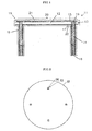
- the semiconductor wafer is put on the region inside the dashed line 1 in Fig. 6.
- the heater center is the first heating region 2 and the outside thereof is the second heating region 3.
- Graphite rod members 4 connected to the first heating region 2 and graphite rod members 5 connected to the second heating region 3 are respectively provided in the most peripheral part of the heater. That is, because the graphite rod members 4 connected to the first heating region 2 located in the vicinity of the heater center are provided in the most peripheral part of the heater, the conductive pathways 6 connecting the first heating region 2 and the graphite rod members 4 have to be provided in the second heating region 3.
- the conductive pathway 6 becomes a local heating part or a local low-temperature part. Therefore, there is a problem that temperature distribution of the wafer is adversely affected thereby.
- the present invention has been accomplished to solve the above-mentioned problems, and a main object of the present invention is to provide a ceramic heater by which an object to be heated being directly put thereon can be heated uniformly and of which heating efficiency is high and in which the heater main body is not large in size and is compact, and a method for producing the ceramic heater.
- the heater main body does not become large in size and has a compact structure.
- the ceramic heater can heat uniformly an object to be heated being put directly on the flat heater with high heating efficiency.
- the plate member is made of any one of pyrolytic boron nitride, pyrolytic boron nitride containing carbon, pyrolytic boron nitride containing silicon, and pyrolytic boron nitride containing aluminum.
- the plate member is made of any one of pyrolytic boron nitride and pyrolytic boron nitride containing carbon and pyrolytic boron nitride containing silicon and pyrolytic boron nitride containing aluminum
- the plate member can be produced by chemical vapor deposition method and can be stably used at a high temperature, and therefore there is no scattering of impurities and therefore the heater is applicable to heating process in which high purity is required.
- the plate member is made of pyrolytic boron nitride containing carbon or pyrolytic boron nitride containing silicon or pyrolytic boron nitride containing aluminum
- resistivity of the plate member becomes smaller as the carbon content or the silicon content or the aluminum content becomes larger. It is necessary that the carbon content or the silicon content or the aluminum content is suppressed to amount by which insulation can be held at gaps of the heater pattern.
- the rod member is made of any one of graphite, sintered silicon carbide, and sintered boron carbide.
- the conductive layer is made of any one of pyrolytic graphite and pyrolytic graphite containing boron and/or boron carbide.
- the conductive layer is made of any one of pyrolytic graphite and pyrolytic graphite containing boron and/or boron carbide
- the conductive layer is easier to be processed than metal foil or rolled circuit and therefore it becomes easy that as the heater pattern having meandering pattern, width and thickness thereof are changed and thereby to make a discretionary temperature gradient therein or to make a heating distribution therein according to the heat environment to uniform heat.
- the thickness of the conductive layer can be more uniform, compared to a method of coating a conductive paste by screen-printing.
- the coating layer is made of any one of pyrolytic boron nitride, pyrolytic boron nitride containing carbon, pyrolytic boron nitride containing silicon, and pyrolytic boron nitride containing aluminum.
- the coating layer is made of any one of pyrolytic boron nitride and pyrolytic boron nitride containing carbon and pyrolytic boron nitride containing silicon and pyrolytic boron nitride containing aluminum, there are no delamination and no scattering of impurities due to use at a high temperature, and therefore, the coating layer becomes applicable to heating process in which high purity is required.
- the coating layer is made of pyrolytic boron nitride containing carbon or pyrolytic boron nitride containing silicon or pyrolytic boron nitride containing aluminum
- resistivity of the coating layer becomes smaller as the carbon content or the silicon content or the aluminum content becomes larger. It is necessary that the carbon content or the silicon content or the aluminum content is suppressed to amount by which insulation can be held at gaps of the heater pattern or between the heater pattern and the object to be heated.
- the present invention provides a method for producing a ceramic heater, comprising at least steps of:
- the rod member and the plate member can be firmly fixed.
- the rod member and the plate member can be firmly fixed easily and it is not necessary to use screw and such.
- the heater pattern is formed by processing the conductive layer on the main surface of the plate member having the same plane and the conductive layer on the opposite main surface of the plate member is partially or totally removed and thereby to insulate electrically the rod members not to be short-circuited to each other, and thereby there can be easily produced a heater by which heating can be performed uniformly with high heating efficiency.
- the rod member and the plate member can be easily fixed, for example, along with forming the coating layer by chemical vapor deposition method.
- the rod member is inserted into the through-hole of the plate member by press-fit.
- the rod member When the rod member is inserted into the through-hole of the plate member by press-fit, screw is not used for connecting the plate member and the rod member, and the contact of the conductive layer and the rod member can be good and cross-section area of the rod member can be small. Therefore, amount of heat to outflow to the outside can be suppressed to small and the object to be heated can be heated uniformly with higher heating efficiency.
- the plate member When any one of pyrolytic boron nitride and pyrolytic boron nitride containing carbon and pyrolytic boron nitride containing silicon and pyrolytic boron nitride containing aluminum is used as the plate member, the plate member can be produced by chemical vapor deposition method and there is no scattering of impurities due to use at a high temperature, and therefore, there can be produced a heater being also applicable to heating process in which high purity is required.
- the plate member is made of pyrolytic boron nitride containing carbon or pyrolytic boron nitride containing silicon or pyrolytic boron nitride containing aluminum
- resistivity of the plate member becomes smaller as the carbon content or the silicon content or the aluminum content becomes larger. It is necessary that the carbon content or the silicon content or the aluminum content is suppressed to amount by which insulation can be held at gaps of the heater pattern.
- the conductive layer is formed by chemically vapor-depositing any one of pyrolytic graphite and pyrolytic graphite containing boron and/or boron carbide.
- the coating layer is formed by chemically vapor-depositing any one of pyrolytic boron nitride, pyrolytic boron nitride containing carbon, pyrolytic boron nitride containing silicon, and pyrolytic boron nitride containing aluminum.
- the coating layer is made of pyrolytic boron nitride containing carbon or pyrolytic boron nitride containing silicon or pyrolytic boron nitride containing aluminum
- resistivity of the coating layer becomes smaller as the carbon content or the silicon content or the aluminum content becomes larger. It is necessary that the carbon content or the silicon content or the aluminum content is suppressed to amount by which insulation can be held at gaps of the heater pattern or between the heater pattern and the object to be heated.
- the contact of the conductive layer and the rod member is good and also endurance thereof is also high and also cross-section area of the rod member can become small, and therefore, the object to be heated can be heated uniformly with higher heating efficiency.
- the present inventors have investigated thoroughly. They have found that by the following ceramic heater, an object to be heated being directly put on a flat heater can be heated uniformly and heating efficiency thereof is high and the heater main body is not large in size and is compact.
- the present invention provides a ceramic heater comprising: at least
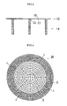
- Fig. 1 is a view showing an example of a ceramic heater of the present invention.
- Fig. 2 and 3 show an example of a plate member and a rod member in the ceramic heater of the present invention.
- the present invention provides a ceramic heater 11 comprising: at least
- the ceramic heater can be smaller in size than a conventional one and the heater can be flat without sticking-out thing on the heating surface of the heater.
- the ceramic heater can heat uniformly an object to be heated being put directly on the flat heater with high heating efficiency.
- a heater pattern 20 is also formed on one end face 16 of the rod member 14.
- the rod members 14 are electrically insulated not to be short-circuited to each other in a main surface 17 of the plate member 12 opposite to a side on which the heater pattern is formed.
- the conductive layer on the opposite surface may be partially or totally removed. In Fig. 1, the conductive layer is partially removed by forming a groove 22.
- the plate member 12 is made of insulating ceramics in which one or more pair(s) of through-holes 13 are formed and functions as a supporting substrate in which a heater pattern 20 is formed.
- the plate member is made of any one of pyrolytic boron nitride, pyrolytic boron nitride containing carbon, pyrolytic boron nitride containing silicon, and pyrolytic boron nitride containing aluminum.
- the plate member 12 can be produced by chemical vapor deposition method and has a high insulating property and there is no scattering of impurities due to use at a high temperature, and therefore is applicable to heating process in which high purity is required. In particular, it can be also used stably in a high-temperature process at about 1500 °C and additionally at a rapidly rising or falling temperature of 100 °C/min or more. It is preferable that thickness of the plate member 12 is 1-5 mm, and more preferably, 2-4 mm. In the case that the thickness of the plate member 12 is thinner than 1 mm, bow is occasionally caused.
- the rod member 14 has a power-supply terminal 18 to be supplied with power source at one end thereof and is inserted into the through-hole 13 of the plate member 12 at another end thereof and is made of conductive ceramics, and one end face 16 opposite to a side having the power-supply terminal 18 has a same plane with a main surface 15 of the plate member.
- the heater main body does not become large in size and has a compact structure. And, there can be produced a heater being capable of heating uniformly an object to be heated being put directly on the flat heater with high heating efficiency by the heater pattern to be formed on the same plane.
- the rod member 14 is pressed-fit into the through-hole 13 of the plate member 12 and fixed by being coated with the conductive layer 19 and the coating layer 21.
- this can be formed by pressing-fit the rod members 14 into the plate member 12 and then performing flat-surface processing by subjecting the main surface 15 of the plate member and the one end face 16 to flat-surface grinding or the like so that the end face has the same plane with the main surface 15.
- this has a structure being fixed without using screw for connecting the plate member and the rod member.
- the rod member 14 made of conductive ceramics is made to be thick for an object of preventing the trouble in the screw ridges as a conventional technique, cross-section area of the rod member 14 can be small. Therefore, amount of heat to outflow to the outside can be suppressed to small and the object to be heated can be heated uniformly with higher heating efficiency.
- the rod member 14 is made of any one of graphite, sintered silicon carbide, and sintered boron carbide.
- the rod member becomes excellent in heat resistance and additionally the outer face thereof are coated with the conductive layer and the coating layer, and therefore, there is no scattering of impurities and therefore the heater is applicable to heating process in which high purity is required.
- graphite is more preferable because it is relatively low in price and easy to be processed.
- a shape of the rod member 14 is a cylindrical shape as shown in Fig. 1 or 3.
- the shape is not limited thereto and may be a shape being capable of being inserted and fixed to the through-hole 13.
- Diameter of the rod member 14 is not particularly limited. However, it may be a diameter of 3-20 mm and more preferably 8-14 mm. If the diameter is smaller than 3 mm, the rod member occasionally breaks. If the diameter is larger than 20 mm, outflow of heat to the outside from the rod member 14 is large and temperature distribution of the heater occasionally becomes large.
- the conductive layer 19 coats and fixes the plate member 12 and the rod member 14 pressed-fit into the through-hole 13 therein. Thereby, the rod member 14 and the plate member 12 can be firmly fixed, and the electrical contact of the conductive layer and the rod member can be good.
- the conductive layer 19 is made of any one of pyrolytic graphite and pyrolytic graphite containing boron and/or boron carbide.
- the heater can be stably used until a high temperature, and the conductive layer is easier to be processed than metal foil or rolled circuit and therefore it becomes easy that as the heater pattern having meandering pattern, width and thickness thereof are changed and thereby to make a discretionary temperature gradient therein or to make a heating distribution therein according to the heat environment to uniform heat.
- the thickness of the conductive layer can be more uniform, compared to a method of coating a conductive paste by screen-printing.
- the thickness of the conductive layer 19 is not particularly limited. However, it is desirable that the thickness is 10-300 ⁇ m and particularly 30-150 ⁇ m. It is sufficient that an appropriate thickness is selected well-considering the relation of the electric capacity or the shape of the heater pattern 20 for making the heater temperature reach an objective temperature and uniform heat.
- the conductive layer 19 on the surface 16 of the rod member having the same plane and on the main surface 15 of the plate member is processed and thereby the heater pattern 20 is formed.
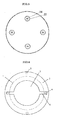
- the heater pattern 20 is formed so that one pair of the rod members can supply current in the pattern forming the first heating region 2 shown as the inner white part and the other pair of the rod members can supply current in the pattern forming the second heating region 3 shown as the outer gray part.
- a large heater has become used as a heater for heating such a wafer.
- a heater pattern which has two-zone system as described above or which is divided into more regions. However, it is not necessarily limited thereto.
- the rod members 14 are electrically insulated not to be short-circuited to each other.
- the electrical insulating can be performed easily.
- the heater being capable of uniform heating with high heating efficiency can be produced by processing the conductive layer 19 on the surface 16 of the rod member and the main surface 15 of the plate member which have the same plane and thereby forming the heater pattern 20 and removing partially or totally the conductive layer 19 on the opposite main surface 17 of the plate member 12 and thereby electrically insulating the rod members 14 not to be short-circuited to each other.
- the coating layer 21 is made of insulating ceramics formed on the conductive layer 19 and made of any one of pyrolytic boron nitride, pyrolytic boron nitride containing carbon, pyrolytic boron nitride containing silicon, and pyrolytic boron nitride containing aluminum.
- the coating layer becomes applicable to heating process in which high purity is required.
- it can be also used stably in a high-temperature process at about 1500 °C and additionally at a rapidly rising or falling temperature of 100 °C/min or more.
- the coating layer is made of pyrolytic boron nitride containing carbon or pyrolytic boron nitride containing silicon or pyrolytic boron nitride containing aluminum
- resistivity of the coating layer becomes smaller as the carbon content or the silicon content or the aluminum content becomes larger. It is necessary that the carbon content or the silicon content or the aluminum content is suppressed to amount by which insulation can be held at gaps of the heater pattern or between the heater pattern and the object to be heated.
- the thickness of the coating layer 21 is not particularly limited. However, it is desirable that the thickness is 20-300 ⁇ m and particularly 50-200 ⁇ m. If the thickness of the coating layer 21 is thicker than 20 ⁇ m, there is not a risk of dielectric breakdown or the like, and if the thickness is thinner than 300 ⁇ m, delamination or the like is not caused.
- the coating layer 21 is being formed by chemical vapor deposition method and at the same time the rod member and the plate member can be easily fixed.
- Such a ceramic heater 11 according to the present invention can be produced by a method for producing a ceramic heater, comprising at least steps of:
- a ceramic heater according to the present invention in which the heater main body is not large in size and has a compact structure and by which an object to be heated being directly put on a flat heater can be heated uniformly with high heating efficiency can be easily produced at low cost.
- the plate member made of pyrolytic boron nitride having a diameter of 310 mm and a thickness of 2.5 mm was produced by reacting 4 SLM of ammonium and 2 SLM of boron trichloride under a pressure of 10 Torr at a temperature of 1850 °C.
- the through-holes having a 12 mm diameter were provided in two places on a 102 mm radius from the center of this plate member and in two places on a 111 mm radius therefrom.
- a pyrolytic graphite layer containing boron carbide having a thickness of 50 ⁇ m was provided by pyrolyzing 3 SLM of methane and 0.1 SLM of boron trichloride under a pressure of 5 Torr at a temperature of 1750 °C, the heater pattern as Fig. 4 was formed by machining therein, and thereby, this was made to be a ceramic heater having two-zone system.
- the first heating region in the central part of the heater and the second heating region located in the outside thereof were divided at the part of a 108.8 mm radius as shown as "A" in Fig. 4.
- the first heating region had an almost concentric shape and the second heating region had a ring shape.
- the ceramic heater according to the present invention even if it is a heater for heating a semiconductor wafer having a large diameter of 300 mm (12 inches), it is not necessary that the positions in which the rod members are provided are made to be outside the region on the plate member on which a semiconductor wafer is put, and therefore, the heater main body does not become large in size and has a compact structure whose diameter is only about 310 mm.
- the ceramic heater can heat uniformly an object to be heated with high heating efficiency.
Landscapes
- Chemical & Material Sciences (AREA)
- Engineering & Computer Science (AREA)
- Ceramic Engineering (AREA)
- Resistance Heating (AREA)
- Surface Heating Bodies (AREA)
Applications Claiming Priority (1)
| Application Number | Priority Date | Filing Date | Title |
|---|---|---|---|
| JP2005323967A JP2007134088A (ja) | 2005-11-08 | 2005-11-08 | セラミックスヒーターおよびセラミックスヒーターの製造方法 |
Publications (3)
| Publication Number | Publication Date |
|---|---|
| EP1784050A2 true EP1784050A2 (de) | 2007-05-09 |
| EP1784050A3 EP1784050A3 (de) | 2008-09-24 |
| EP1784050B1 EP1784050B1 (de) | 2015-09-02 |
Family
ID=37547500
Family Applications (1)
| Application Number | Title | Priority Date | Filing Date |
|---|---|---|---|
| EP06255610.5A Not-in-force EP1784050B1 (de) | 2005-11-08 | 2006-10-31 | Keramisches Heizelement und Verfahren zur Herstellung von keramischen Heizern. |
Country Status (5)
| Country | Link |
|---|---|
| US (1) | US7329842B2 (de) |
| EP (1) | EP1784050B1 (de) |
| JP (1) | JP2007134088A (de) |
| KR (1) | KR101299496B1 (de) |
| TW (1) | TWI350122B (de) |
Cited By (1)
| Publication number | Priority date | Publication date | Assignee | Title |
|---|---|---|---|---|
| CN104427666A (zh) * | 2013-08-21 | 2015-03-18 | 信越化学工业株式会社 | 立体形状的陶瓷加热器 |
Families Citing this family (17)
| Publication number | Priority date | Publication date | Assignee | Title |
|---|---|---|---|---|
| KR101299495B1 (ko) * | 2005-12-08 | 2013-08-29 | 신에쓰 가가꾸 고교 가부시끼가이샤 | 세라믹스 히터, 히터 급전 부품 및 세라믹스 히터의제조방법 |
| JP2009123577A (ja) * | 2007-11-16 | 2009-06-04 | Ulvac Japan Ltd | 基板加熱装置 |
| JP2009301796A (ja) * | 2008-06-11 | 2009-12-24 | Shin-Etsu Chemical Co Ltd | セラミックスヒーター及びその製造方法 |
| AU2009316245A1 (en) * | 2008-11-14 | 2010-05-20 | Quickir Cuisine Pty Ltd | A cooking apparatus with non-metal plates |
| JP5894401B2 (ja) * | 2011-09-12 | 2016-03-30 | モメンティブ・パフォーマンス・マテリアルズ・ジャパン合同会社 | ポスト型セラミックスヒータおよびその製造方法 |
| JP5996519B2 (ja) * | 2013-03-13 | 2016-09-21 | 信越化学工業株式会社 | セラミックヒーター |
| US10154542B2 (en) * | 2015-10-19 | 2018-12-11 | Watlow Electric Manufacturing Company | Composite device with cylindrical anisotropic thermal conductivity |
| CN107059112B (zh) * | 2017-04-14 | 2023-12-08 | 南京晶能半导体科技有限公司 | 半导体级硅单晶炉底部加热器 |
| KR101989855B1 (ko) * | 2017-04-18 | 2019-06-17 | 주식회사 아모센스 | 궐련형 전자담배장치용 발열히터 |
| JP2019060819A (ja) * | 2017-09-28 | 2019-04-18 | 日本特殊陶業株式会社 | 電子部品検査装置用配線基板 |
| US10681778B2 (en) * | 2017-11-21 | 2020-06-09 | Watlow Electric Manufacturing Company | Integrated heater and method of manufacture |
| US11083050B2 (en) | 2017-11-21 | 2021-08-03 | Watlow Electric Manufacturing Company | Integrated heater and method of manufacture |
| TWI697253B (zh) * | 2018-05-22 | 2020-06-21 | 美商瓦特洛威電子製造公司 | 一體式加熱器及製造方法 |
| JP7175324B2 (ja) * | 2018-09-28 | 2022-11-18 | 京セラ株式会社 | セラミック構造体及びウェハ用システム |
| WO2020090379A1 (ja) * | 2018-10-30 | 2020-05-07 | 京セラ株式会社 | 基板状構造体及びヒータシステム |
| US12114402B2 (en) * | 2018-11-19 | 2024-10-08 | Niterra Co., Ltd. | Holding device and method of manufacturing holding device |
| CN113271692B (zh) * | 2021-04-29 | 2023-01-17 | 苏州极限深灰光电科技有限公司 | 陶瓷发热体、方法、红外加热管及设备 |
Family Cites Families (13)
| Publication number | Priority date | Publication date | Assignee | Title |
|---|---|---|---|---|
| US5343022A (en) * | 1992-09-29 | 1994-08-30 | Advanced Ceramics Corporation | Pyrolytic boron nitride heating unit |
| JP2984164B2 (ja) * | 1993-03-26 | 1999-11-29 | 日本碍子株式会社 | 半導体製造用サセプター |
| JPH10189227A (ja) * | 1996-12-27 | 1998-07-21 | Shin Etsu Chem Co Ltd | 加熱ユニットおよびその接続方法 |
| JP3560456B2 (ja) * | 1997-12-11 | 2004-09-02 | 信越化学工業株式会社 | 複層セラミックスヒータ |
| JP3477062B2 (ja) * | 1997-12-26 | 2003-12-10 | 京セラ株式会社 | ウエハ加熱装置 |
| JP3914377B2 (ja) * | 2000-07-17 | 2007-05-16 | 信越化学工業株式会社 | 静電吸着機能を有するウエーハ加熱装置 |
| JP4521107B2 (ja) * | 2000-10-17 | 2010-08-11 | 株式会社ブリヂストン | ヒータ及び半導体製造装置 |
| JP2002313531A (ja) * | 2001-04-17 | 2002-10-25 | Toshiba Ceramics Co Ltd | 面状セラミックスヒーター及び製造方法 |
| JP2002313539A (ja) * | 2001-04-17 | 2002-10-25 | Toshiba Ceramics Co Ltd | 面状セラミックスヒーター及びその製造方法 |
| US20040074898A1 (en) * | 2002-10-21 | 2004-04-22 | Mariner John T. | Encapsulated graphite heater and process |
| JP2004220966A (ja) | 2003-01-16 | 2004-08-05 | Ngk Insulators Ltd | ヒーターおよびその製造方法 |
| JP4602662B2 (ja) * | 2003-12-01 | 2010-12-22 | 株式会社ブリヂストン | セラミックヒータユニット |
| JP2004253799A (ja) | 2004-02-16 | 2004-09-09 | Ibiden Co Ltd | 半導体製造・検査装置 |
-
2005
- 2005-11-08 JP JP2005323967A patent/JP2007134088A/ja active Pending
-
2006
- 2006-09-08 KR KR1020060086782A patent/KR101299496B1/ko not_active Expired - Fee Related
- 2006-10-24 TW TW095139238A patent/TWI350122B/zh not_active IP Right Cessation
- 2006-10-31 EP EP06255610.5A patent/EP1784050B1/de not_active Not-in-force
- 2006-11-01 US US11/590,812 patent/US7329842B2/en not_active Expired - Fee Related
Cited By (2)
| Publication number | Priority date | Publication date | Assignee | Title |
|---|---|---|---|---|
| CN104427666A (zh) * | 2013-08-21 | 2015-03-18 | 信越化学工业株式会社 | 立体形状的陶瓷加热器 |
| CN104427666B (zh) * | 2013-08-21 | 2016-02-10 | 信越化学工业株式会社 | 立体形状的陶瓷加热器 |
Also Published As
| Publication number | Publication date |
|---|---|
| KR101299496B1 (ko) | 2013-08-29 |
| JP2007134088A (ja) | 2007-05-31 |
| US20070102419A1 (en) | 2007-05-10 |
| KR20070049543A (ko) | 2007-05-11 |
| TW200735690A (en) | 2007-09-16 |
| EP1784050A3 (de) | 2008-09-24 |
| US7329842B2 (en) | 2008-02-12 |
| TWI350122B (en) | 2011-10-01 |
| EP1784050B1 (de) | 2015-09-02 |
Similar Documents
| Publication | Publication Date | Title |
|---|---|---|
| EP1784050B1 (de) | Keramisches Heizelement und Verfahren zur Herstellung von keramischen Heizern. | |
| US6242719B1 (en) | Multiple-layered ceramic heater | |
| KR102193401B1 (ko) | 입체 형상의 세라믹스 히터 | |
| EP1799014B1 (de) | Keramischer Heizer, Verfahren zur Herstellung eines keramischen Heizers und Heizerstromversorgungsbauteil | |
| KR101371004B1 (ko) | 가열소자 | |
| EP0929204B1 (de) | Keramisches Heizelement | |
| KR19980063671A (ko) | 기판의 균일 가열을 위한 기판 지지부재 | |
| US7053339B2 (en) | Ceramic heater | |
| KR102087640B1 (ko) | 세라믹 히터 | |
| JP3145664B2 (ja) | ウエハ加熱装置 | |
| KR20150006405A (ko) | 내부식성 적층 세라믹스 부재 | |
| JP7103340B2 (ja) | セラミックスヒータ | |
| JP3560456B2 (ja) | 複層セラミックスヒータ | |
| JP2007157661A (ja) | セラミックスヒーターおよびセラミックスヒーターの製造方法 | |
| JP2001338862A (ja) | ウエハ加熱装置 | |
| JP2002110524A (ja) | ウエハ加熱装置 | |
| JP2007250403A (ja) | セラミックスヒーターおよびヒーター給電部品 | |
| JP2001189276A (ja) | ウエハ加熱装置 | |
| JP3906026B2 (ja) | ウエハ加熱装置 | |
| JP4000236B2 (ja) | セラミックスヒータ | |
| JP2001357964A (ja) | 複層セラミックスヒーター | |
| JP2005011769A (ja) | 窒化アルミニウムのセラミックスヒータ | |
| WO2025046907A1 (ja) | ウエハ支持台及びrfロッド | |
| JP2001237166A (ja) | ウエハ加熱装置 | |
| JP2004296578A (ja) | ウェハ支持部材 |
Legal Events
| Date | Code | Title | Description |
|---|---|---|---|
| PUAI | Public reference made under article 153(3) epc to a published international application that has entered the european phase |
Free format text: ORIGINAL CODE: 0009012 |
|
| AK | Designated contracting states |
Kind code of ref document: A2 Designated state(s): AT BE BG CH CY CZ DE DK EE ES FI FR GB GR HU IE IS IT LI LT LU LV MC NL PL PT RO SE SI SK TR |
|
| AX | Request for extension of the european patent |
Extension state: AL BA HR MK YU |
|
| PUAL | Search report despatched |
Free format text: ORIGINAL CODE: 0009013 |
|
| AK | Designated contracting states |
Kind code of ref document: A3 Designated state(s): AT BE BG CH CY CZ DE DK EE ES FI FR GB GR HU IE IS IT LI LT LU LV MC NL PL PT RO SE SI SK TR |
|
| AX | Request for extension of the european patent |
Extension state: AL BA HR MK RS |
|
| AKX | Designation fees paid | ||
| REG | Reference to a national code |
Ref country code: DE Ref legal event code: 8566 |
|
| 17P | Request for examination filed |
Effective date: 20090312 |
|
| RBV | Designated contracting states (corrected) |
Designated state(s): DE FR GB |
|
| 17Q | First examination report despatched |
Effective date: 20110524 |
|
| GRAP | Despatch of communication of intention to grant a patent |
Free format text: ORIGINAL CODE: EPIDOSNIGR1 |
|
| INTG | Intention to grant announced |
Effective date: 20150413 |
|
| GRAS | Grant fee paid |
Free format text: ORIGINAL CODE: EPIDOSNIGR3 |
|
| GRAA | (expected) grant |
Free format text: ORIGINAL CODE: 0009210 |
|
| AK | Designated contracting states |
Kind code of ref document: B1 Designated state(s): DE FR GB |
|
| REG | Reference to a national code |
Ref country code: GB Ref legal event code: FG4D |
|
| REG | Reference to a national code |
Ref country code: FR Ref legal event code: PLFP Year of fee payment: 10 |
|
| REG | Reference to a national code |
Ref country code: DE Ref legal event code: R096 Ref document number: 602006046489 Country of ref document: DE |
|
| PGFP | Annual fee paid to national office [announced via postgrant information from national office to epo] |
Ref country code: FR Payment date: 20150923 Year of fee payment: 10 |
|
| PGFP | Annual fee paid to national office [announced via postgrant information from national office to epo] |
Ref country code: GB Payment date: 20151028 Year of fee payment: 10 |
|
| REG | Reference to a national code |
Ref country code: DE Ref legal event code: R097 Ref document number: 602006046489 Country of ref document: DE |
|
| PLBE | No opposition filed within time limit |
Free format text: ORIGINAL CODE: 0009261 |
|
| STAA | Information on the status of an ep patent application or granted ep patent |
Free format text: STATUS: NO OPPOSITION FILED WITHIN TIME LIMIT |
|
| 26N | No opposition filed |
Effective date: 20160603 |
|
| GBPC | Gb: european patent ceased through non-payment of renewal fee |
Effective date: 20161031 |
|
| REG | Reference to a national code |
Ref country code: FR Ref legal event code: ST Effective date: 20170630 |
|
| PG25 | Lapsed in a contracting state [announced via postgrant information from national office to epo] |
Ref country code: GB Free format text: LAPSE BECAUSE OF NON-PAYMENT OF DUE FEES Effective date: 20161031 Ref country code: FR Free format text: LAPSE BECAUSE OF NON-PAYMENT OF DUE FEES Effective date: 20161102 |
|
| PGFP | Annual fee paid to national office [announced via postgrant information from national office to epo] |
Ref country code: DE Payment date: 20181016 Year of fee payment: 13 |
|
| REG | Reference to a national code |
Ref country code: DE Ref legal event code: R119 Ref document number: 602006046489 Country of ref document: DE |
|
| PG25 | Lapsed in a contracting state [announced via postgrant information from national office to epo] |
Ref country code: DE Free format text: LAPSE BECAUSE OF NON-PAYMENT OF DUE FEES Effective date: 20200501 |