EP1760699A1 - Substrat für ein magnetisches Informationsaufzeichnungsmedium und Verfahren zur Substratherstellung für ein magnetisches Informationsaufzeichnungsmedium - Google Patents
Substrat für ein magnetisches Informationsaufzeichnungsmedium und Verfahren zur Substratherstellung für ein magnetisches Informationsaufzeichnungsmedium Download PDFInfo
- Publication number
- EP1760699A1 EP1760699A1 EP06254457A EP06254457A EP1760699A1 EP 1760699 A1 EP1760699 A1 EP 1760699A1 EP 06254457 A EP06254457 A EP 06254457A EP 06254457 A EP06254457 A EP 06254457A EP 1760699 A1 EP1760699 A1 EP 1760699A1
- Authority
- EP
- European Patent Office
- Prior art keywords
- base plate
- substrate
- resin
- layer
- covering layer
- Prior art date
- Legal status (The legal status is an assumption and is not a legal conclusion. Google has not performed a legal analysis and makes no representation as to the accuracy of the status listed.)
- Withdrawn
Links
- 239000000758 substrate Substances 0.000 title claims abstract description 167
- 238000000034 method Methods 0.000 title claims abstract description 61
- 229920005989 resin Polymers 0.000 claims abstract description 286
- 239000011347 resin Substances 0.000 claims abstract description 286
- 239000000463 material Substances 0.000 claims abstract description 59
- 239000010410 layer Substances 0.000 claims description 330
- 239000002245 particle Substances 0.000 claims description 81
- 230000003746 surface roughness Effects 0.000 claims description 65
- 238000005498 polishing Methods 0.000 claims description 28
- 239000011521 glass Substances 0.000 claims description 26
- 238000000465 moulding Methods 0.000 claims description 26
- 238000001746 injection moulding Methods 0.000 claims description 20
- PXHVJJICTQNCMI-UHFFFAOYSA-N nickel Substances [Ni] PXHVJJICTQNCMI-UHFFFAOYSA-N 0.000 claims description 16
- KDLHZDBZIXYQEI-UHFFFAOYSA-N palladium Substances [Pd] KDLHZDBZIXYQEI-UHFFFAOYSA-N 0.000 claims description 12
- OKTJSMMVPCPJKN-UHFFFAOYSA-N Carbon Chemical compound [C] OKTJSMMVPCPJKN-UHFFFAOYSA-N 0.000 claims description 9
- XEEYBQQBJWHFJM-UHFFFAOYSA-N iron Substances [Fe] XEEYBQQBJWHFJM-UHFFFAOYSA-N 0.000 claims description 9
- 229910052751 metal Inorganic materials 0.000 claims description 9
- 239000002184 metal Substances 0.000 claims description 9
- 238000000748 compression moulding Methods 0.000 claims description 8
- 239000010936 titanium Substances 0.000 claims description 8
- 239000011701 zinc Substances 0.000 claims description 8
- 239000010949 copper Substances 0.000 claims description 6
- 230000009477 glass transition Effects 0.000 claims description 6
- 239000011572 manganese Substances 0.000 claims description 6
- 229910052710 silicon Inorganic materials 0.000 claims description 6
- 239000010703 silicon Substances 0.000 claims description 6
- KRHYYFGTRYWZRS-UHFFFAOYSA-M Fluoride anion Chemical compound [F-] KRHYYFGTRYWZRS-UHFFFAOYSA-M 0.000 claims description 5
- UCKMPCXJQFINFW-UHFFFAOYSA-N Sulphide Chemical compound [S-2] UCKMPCXJQFINFW-UHFFFAOYSA-N 0.000 claims description 5
- 229910052799 carbon Inorganic materials 0.000 claims description 5
- 239000000919 ceramic Substances 0.000 claims description 5
- CPELXLSAUQHCOX-UHFFFAOYSA-M Bromide Chemical compound [Br-] CPELXLSAUQHCOX-UHFFFAOYSA-M 0.000 claims description 4
- XMWRBQBLMFGWIX-UHFFFAOYSA-N C60 fullerene Chemical compound C12=C3C(C4=C56)=C7C8=C5C5=C9C%10=C6C6=C4C1=C1C4=C6C6=C%10C%10=C9C9=C%11C5=C8C5=C8C7=C3C3=C7C2=C1C1=C2C4=C6C4=C%10C6=C9C9=C%11C5=C5C8=C3C3=C7C1=C1C2=C4C6=C2C9=C5C3=C12 XMWRBQBLMFGWIX-UHFFFAOYSA-N 0.000 claims description 4
- 229920000049 Carbon (fiber) Polymers 0.000 claims description 4
- BVKZGUZCCUSVTD-UHFFFAOYSA-L Carbonate Chemical compound [O-]C([O-])=O BVKZGUZCCUSVTD-UHFFFAOYSA-L 0.000 claims description 4
- VEXZGXHMUGYJMC-UHFFFAOYSA-M Chloride anion Chemical compound [Cl-] VEXZGXHMUGYJMC-UHFFFAOYSA-M 0.000 claims description 4
- 229910002651 NO3 Inorganic materials 0.000 claims description 4
- NHNBFGGVMKEFGY-UHFFFAOYSA-N Nitrate Chemical compound [O-][N+]([O-])=O NHNBFGGVMKEFGY-UHFFFAOYSA-N 0.000 claims description 4
- 229910019142 PO4 Inorganic materials 0.000 claims description 4
- QAOWNCQODCNURD-UHFFFAOYSA-L Sulfate Chemical compound [O-]S([O-])(=O)=O QAOWNCQODCNURD-UHFFFAOYSA-L 0.000 claims description 4
- ATJFFYVFTNAWJD-UHFFFAOYSA-N Tin Chemical compound [Sn] ATJFFYVFTNAWJD-UHFFFAOYSA-N 0.000 claims description 4
- RTAQQCXQSZGOHL-UHFFFAOYSA-N Titanium Chemical compound [Ti] RTAQQCXQSZGOHL-UHFFFAOYSA-N 0.000 claims description 4
- HCHKCACWOHOZIP-UHFFFAOYSA-N Zinc Chemical compound [Zn] HCHKCACWOHOZIP-UHFFFAOYSA-N 0.000 claims description 4
- 239000004917 carbon fiber Substances 0.000 claims description 4
- 239000002041 carbon nanotube Substances 0.000 claims description 4
- 229910021393 carbon nanotube Inorganic materials 0.000 claims description 4
- 229910003472 fullerene Inorganic materials 0.000 claims description 4
- 239000003365 glass fiber Substances 0.000 claims description 4
- 238000002347 injection Methods 0.000 claims description 4
- 239000007924 injection Substances 0.000 claims description 4
- VNWKTOKETHGBQD-UHFFFAOYSA-N methane Chemical compound C VNWKTOKETHGBQD-UHFFFAOYSA-N 0.000 claims description 4
- 150000004767 nitrides Chemical class 0.000 claims description 4
- 229910052763 palladium Inorganic materials 0.000 claims description 4
- 230000002093 peripheral effect Effects 0.000 claims description 4
- NBIIXXVUZAFLBC-UHFFFAOYSA-K phosphate Chemical compound [O-]P([O-])([O-])=O NBIIXXVUZAFLBC-UHFFFAOYSA-K 0.000 claims description 4
- 239000010452 phosphate Substances 0.000 claims description 4
- 239000004065 semiconductor Substances 0.000 claims description 4
- 229910052719 titanium Inorganic materials 0.000 claims description 4
- 229910052725 zinc Inorganic materials 0.000 claims description 4
- RYGMFSIKBFXOCR-UHFFFAOYSA-N Copper Chemical compound [Cu] RYGMFSIKBFXOCR-UHFFFAOYSA-N 0.000 claims description 3
- GYHNNYVSQQEPJS-UHFFFAOYSA-N Gallium Chemical compound [Ga] GYHNNYVSQQEPJS-UHFFFAOYSA-N 0.000 claims description 3
- PWHULOQIROXLJO-UHFFFAOYSA-N Manganese Chemical compound [Mn] PWHULOQIROXLJO-UHFFFAOYSA-N 0.000 claims description 3
- OAICVXFJPJFONN-UHFFFAOYSA-N Phosphorus Chemical compound [P] OAICVXFJPJFONN-UHFFFAOYSA-N 0.000 claims description 3
- 239000010941 cobalt Substances 0.000 claims description 3
- 229910017052 cobalt Inorganic materials 0.000 claims description 3
- GUTLYIVDDKVIGB-UHFFFAOYSA-N cobalt atom Chemical compound [Co] GUTLYIVDDKVIGB-UHFFFAOYSA-N 0.000 claims description 3
- 229910052802 copper Inorganic materials 0.000 claims description 3
- 229910052733 gallium Inorganic materials 0.000 claims description 3
- 229910052732 germanium Inorganic materials 0.000 claims description 3
- GNPVGFCGXDBREM-UHFFFAOYSA-N germanium atom Chemical compound [Ge] GNPVGFCGXDBREM-UHFFFAOYSA-N 0.000 claims description 3
- 229910052742 iron Inorganic materials 0.000 claims description 3
- 229910052748 manganese Inorganic materials 0.000 claims description 3
- 229910052759 nickel Inorganic materials 0.000 claims description 3
- 239000012044 organic layer Substances 0.000 claims description 3
- 229910052698 phosphorus Inorganic materials 0.000 claims description 3
- 239000011574 phosphorus Substances 0.000 claims description 3
- 239000002131 composite material Substances 0.000 claims description 2
- 239000002585 base Substances 0.000 description 269
- 238000007517 polishing process Methods 0.000 description 22
- 229910052782 aluminium Inorganic materials 0.000 description 17
- XAGFODPZIPBFFR-UHFFFAOYSA-N aluminium Chemical compound [Al] XAGFODPZIPBFFR-UHFFFAOYSA-N 0.000 description 17
- 238000000227 grinding Methods 0.000 description 15
- 239000000956 alloy Substances 0.000 description 12
- 229910045601 alloy Inorganic materials 0.000 description 12
- 239000004925 Acrylic resin Substances 0.000 description 11
- 238000004519 manufacturing process Methods 0.000 description 11
- 230000000694 effects Effects 0.000 description 9
- 238000005530 etching Methods 0.000 description 9
- 239000000126 substance Substances 0.000 description 9
- 238000004544 sputter deposition Methods 0.000 description 8
- 229920001721 polyimide Polymers 0.000 description 7
- 239000004695 Polyether sulfone Substances 0.000 description 6
- 239000004697 Polyetherimide Substances 0.000 description 6
- QVGXLLKOCUKJST-UHFFFAOYSA-N atomic oxygen Chemical compound [O] QVGXLLKOCUKJST-UHFFFAOYSA-N 0.000 description 6
- 238000006243 chemical reaction Methods 0.000 description 6
- 230000007423 decrease Effects 0.000 description 6
- 238000002156 mixing Methods 0.000 description 6
- 229910052760 oxygen Inorganic materials 0.000 description 6
- 239000001301 oxygen Substances 0.000 description 6
- 238000007747 plating Methods 0.000 description 6
- 229920006393 polyether sulfone Polymers 0.000 description 6
- 229920001601 polyetherimide Polymers 0.000 description 6
- 229920000178 Acrylic resin Polymers 0.000 description 5
- VYPSYNLAJGMNEJ-UHFFFAOYSA-N Silicium dioxide Chemical compound O=[Si]=O VYPSYNLAJGMNEJ-UHFFFAOYSA-N 0.000 description 5
- XUIMIQQOPSSXEZ-UHFFFAOYSA-N Silicon Chemical compound [Si] XUIMIQQOPSSXEZ-UHFFFAOYSA-N 0.000 description 5
- 238000004140 cleaning Methods 0.000 description 5
- 125000004122 cyclic group Chemical group 0.000 description 5
- -1 etc.) Polymers 0.000 description 5
- 229920005672 polyolefin resin Polymers 0.000 description 5
- 229920001187 thermosetting polymer Polymers 0.000 description 5
- KAKZBPTYRLMSJV-UHFFFAOYSA-N Butadiene Chemical compound C=CC=C KAKZBPTYRLMSJV-UHFFFAOYSA-N 0.000 description 4
- 229920000106 Liquid crystal polymer Polymers 0.000 description 4
- 239000004642 Polyimide Substances 0.000 description 4
- 239000003822 epoxy resin Substances 0.000 description 4
- 229920000647 polyepoxide Polymers 0.000 description 4
- ZWEHNKRNPOVVGH-UHFFFAOYSA-N 2-Butanone Chemical compound CCC(C)=O ZWEHNKRNPOVVGH-UHFFFAOYSA-N 0.000 description 3
- 239000004696 Poly ether ether ketone Substances 0.000 description 3
- 239000004962 Polyamide-imide Substances 0.000 description 3
- MPIAGWXWVAHQBB-UHFFFAOYSA-N [3-prop-2-enoyloxy-2-[[3-prop-2-enoyloxy-2,2-bis(prop-2-enoyloxymethyl)propoxy]methyl]-2-(prop-2-enoyloxymethyl)propyl] prop-2-enoate Chemical compound C=CC(=O)OCC(COC(=O)C=C)(COC(=O)C=C)COCC(COC(=O)C=C)(COC(=O)C=C)COC(=O)C=C MPIAGWXWVAHQBB-UHFFFAOYSA-N 0.000 description 3
- QXZUUHYBWMWJHK-UHFFFAOYSA-N [Co].[Ni] Chemical compound [Co].[Ni] QXZUUHYBWMWJHK-UHFFFAOYSA-N 0.000 description 3
- 230000006835 compression Effects 0.000 description 3
- 238000007906 compression Methods 0.000 description 3
- 238000005516 engineering process Methods 0.000 description 3
- 239000007789 gas Substances 0.000 description 3
- 229920002312 polyamide-imide Polymers 0.000 description 3
- 229920002530 polyetherether ketone Polymers 0.000 description 3
- 239000009719 polyimide resin Substances 0.000 description 3
- 239000002904 solvent Substances 0.000 description 3
- 229920002803 thermoplastic polyurethane Polymers 0.000 description 3
- VTYYLEPIZMXCLO-UHFFFAOYSA-L Calcium carbonate Chemical compound [Ca+2].[O-]C([O-])=O VTYYLEPIZMXCLO-UHFFFAOYSA-L 0.000 description 2
- PPBRXRYQALVLMV-UHFFFAOYSA-N Styrene Chemical compound C=CC1=CC=CC=C1 PPBRXRYQALVLMV-UHFFFAOYSA-N 0.000 description 2
- GWEVSGVZZGPLCZ-UHFFFAOYSA-N Titan oxide Chemical compound O=[Ti]=O GWEVSGVZZGPLCZ-UHFFFAOYSA-N 0.000 description 2
- NIXOWILDQLNWCW-UHFFFAOYSA-N acrylic acid group Chemical group C(C=C)(=O)O NIXOWILDQLNWCW-UHFFFAOYSA-N 0.000 description 2
- 229920000122 acrylonitrile butadiene styrene Polymers 0.000 description 2
- 239000000853 adhesive Substances 0.000 description 2
- 230000001070 adhesive effect Effects 0.000 description 2
- 238000000137 annealing Methods 0.000 description 2
- 239000012298 atmosphere Substances 0.000 description 2
- 238000007611 bar coating method Methods 0.000 description 2
- 239000003795 chemical substances by application Substances 0.000 description 2
- 239000008119 colloidal silica Substances 0.000 description 2
- 150000001875 compounds Chemical class 0.000 description 2
- 238000010586 diagram Methods 0.000 description 2
- 238000003618 dip coating Methods 0.000 description 2
- 238000009713 electroplating Methods 0.000 description 2
- 238000000605 extraction Methods 0.000 description 2
- PCHJSUWPFVWCPO-UHFFFAOYSA-N gold Chemical compound [Au] PCHJSUWPFVWCPO-UHFFFAOYSA-N 0.000 description 2
- 238000007654 immersion Methods 0.000 description 2
- 239000011777 magnesium Substances 0.000 description 2
- 238000005259 measurement Methods 0.000 description 2
- 239000003973 paint Substances 0.000 description 2
- 239000003504 photosensitizing agent Substances 0.000 description 2
- 229920003207 poly(ethylene-2,6-naphthalate) Polymers 0.000 description 2
- 239000004417 polycarbonate Substances 0.000 description 2
- 229920000515 polycarbonate Polymers 0.000 description 2
- 229920000728 polyester Polymers 0.000 description 2
- 239000011112 polyethylene naphthalate Substances 0.000 description 2
- 229920000642 polymer Polymers 0.000 description 2
- 229920005862 polyol Polymers 0.000 description 2
- 150000003077 polyols Chemical class 0.000 description 2
- 238000007639 printing Methods 0.000 description 2
- KCTAWXVAICEBSD-UHFFFAOYSA-N prop-2-enoyloxy prop-2-eneperoxoate Chemical compound C=CC(=O)OOOC(=O)C=C KCTAWXVAICEBSD-UHFFFAOYSA-N 0.000 description 2
- 229920002050 silicone resin Polymers 0.000 description 2
- 239000002002 slurry Substances 0.000 description 2
- 238000005507 spraying Methods 0.000 description 2
- 229920005992 thermoplastic resin Polymers 0.000 description 2
- NLELYIIJDKQXTL-UHFFFAOYSA-N (2,3-diethoxyphenyl)-phenylmethanone Chemical compound CCOC1=CC=CC(C(=O)C=2C=CC=CC=2)=C1OCC NLELYIIJDKQXTL-UHFFFAOYSA-N 0.000 description 1
- ARXJGSRGQADJSQ-UHFFFAOYSA-N 1-methoxypropan-2-ol Chemical compound COCC(C)O ARXJGSRGQADJSQ-UHFFFAOYSA-N 0.000 description 1
- CURLTUGMZLYLDI-UHFFFAOYSA-N Carbon dioxide Chemical compound O=C=O CURLTUGMZLYLDI-UHFFFAOYSA-N 0.000 description 1
- FYYHWMGAXLPEAU-UHFFFAOYSA-N Magnesium Chemical compound [Mg] FYYHWMGAXLPEAU-UHFFFAOYSA-N 0.000 description 1
- ZOKXTWBITQBERF-UHFFFAOYSA-N Molybdenum Chemical compound [Mo] ZOKXTWBITQBERF-UHFFFAOYSA-N 0.000 description 1
- 229910018104 Ni-P Inorganic materials 0.000 description 1
- 229910018536 Ni—P Inorganic materials 0.000 description 1
- 239000004698 Polyethylene Substances 0.000 description 1
- 239000004734 Polyphenylene sulfide Substances 0.000 description 1
- 239000004793 Polystyrene Substances 0.000 description 1
- 239000004963 Torlon Substances 0.000 description 1
- 229920003997 Torlon® Polymers 0.000 description 1
- 229920004738 ULTEM® Polymers 0.000 description 1
- 229920001646 UPILEX Polymers 0.000 description 1
- 229920001807 Urea-formaldehyde Polymers 0.000 description 1
- 229920004695 VICTREX™ PEEK Polymers 0.000 description 1
- 239000003513 alkali Substances 0.000 description 1
- PNEYBMLMFCGWSK-UHFFFAOYSA-N aluminium oxide Inorganic materials [O-2].[O-2].[O-2].[Al+3].[Al+3] PNEYBMLMFCGWSK-UHFFFAOYSA-N 0.000 description 1
- 229910000147 aluminium phosphate Inorganic materials 0.000 description 1
- 230000003466 anti-cipated effect Effects 0.000 description 1
- 101150059062 apln gene Proteins 0.000 description 1
- 229910052788 barium Inorganic materials 0.000 description 1
- DSAJWYNOEDNPEQ-UHFFFAOYSA-N barium atom Chemical compound [Ba] DSAJWYNOEDNPEQ-UHFFFAOYSA-N 0.000 description 1
- JUPQTSLXMOCDHR-UHFFFAOYSA-N benzene-1,4-diol;bis(4-fluorophenyl)methanone Chemical compound OC1=CC=C(O)C=C1.C1=CC(F)=CC=C1C(=O)C1=CC=C(F)C=C1 JUPQTSLXMOCDHR-UHFFFAOYSA-N 0.000 description 1
- 229910000019 calcium carbonate Inorganic materials 0.000 description 1
- 229910002090 carbon oxide Inorganic materials 0.000 description 1
- 238000005229 chemical vapour deposition Methods 0.000 description 1
- 229910052681 coesite Inorganic materials 0.000 description 1
- 238000007796 conventional method Methods 0.000 description 1
- 229910052593 corundum Inorganic materials 0.000 description 1
- 229910052906 cristobalite Inorganic materials 0.000 description 1
- 238000005520 cutting process Methods 0.000 description 1
- 238000006073 displacement reaction Methods 0.000 description 1
- 238000001704 evaporation Methods 0.000 description 1
- 239000012467 final product Substances 0.000 description 1
- 238000007667 floating Methods 0.000 description 1
- 238000010438 heat treatment Methods 0.000 description 1
- 229910052738 indium Inorganic materials 0.000 description 1
- APFVFJFRJDLVQX-UHFFFAOYSA-N indium atom Chemical compound [In] APFVFJFRJDLVQX-UHFFFAOYSA-N 0.000 description 1
- 239000003999 initiator Substances 0.000 description 1
- 239000010954 inorganic particle Substances 0.000 description 1
- 238000005342 ion exchange Methods 0.000 description 1
- 230000001788 irregular Effects 0.000 description 1
- 229910052746 lanthanum Inorganic materials 0.000 description 1
- FZLIPJUXYLNCLC-UHFFFAOYSA-N lanthanum atom Chemical compound [La] FZLIPJUXYLNCLC-UHFFFAOYSA-N 0.000 description 1
- 238000003754 machining Methods 0.000 description 1
- 229910052749 magnesium Inorganic materials 0.000 description 1
- 229910001635 magnesium fluoride Inorganic materials 0.000 description 1
- 239000006060 molten glass Substances 0.000 description 1
- 229910052750 molybdenum Inorganic materials 0.000 description 1
- 239000011733 molybdenum Substances 0.000 description 1
- 239000000178 monomer Substances 0.000 description 1
- 239000005011 phenolic resin Substances 0.000 description 1
- 229910001392 phosphorus oxide Inorganic materials 0.000 description 1
- 229920003023 plastic Polymers 0.000 description 1
- 239000004033 plastic Substances 0.000 description 1
- 229920002492 poly(sulfone) Polymers 0.000 description 1
- 229920006122 polyamide resin Polymers 0.000 description 1
- 229920001225 polyester resin Polymers 0.000 description 1
- 239000004645 polyester resin Substances 0.000 description 1
- 229920000098 polyolefin Polymers 0.000 description 1
- 229920000069 polyphenylene sulfide Polymers 0.000 description 1
- 229920005990 polystyrene resin Polymers 0.000 description 1
- 239000000047 product Substances 0.000 description 1
- 230000005855 radiation Effects 0.000 description 1
- 150000003839 salts Chemical class 0.000 description 1
- 239000000377 silicon dioxide Substances 0.000 description 1
- 229910052682 stishovite Inorganic materials 0.000 description 1
- 229910052712 strontium Inorganic materials 0.000 description 1
- CIOAGBVUUVVLOB-UHFFFAOYSA-N strontium atom Chemical compound [Sr] CIOAGBVUUVVLOB-UHFFFAOYSA-N 0.000 description 1
- 229910000018 strontium carbonate Inorganic materials 0.000 description 1
- LEDMRZGFZIAGGB-UHFFFAOYSA-L strontium carbonate Chemical compound [Sr+2].[O-]C([O-])=O LEDMRZGFZIAGGB-UHFFFAOYSA-L 0.000 description 1
- 229910052715 tantalum Inorganic materials 0.000 description 1
- GUVRBAGPIYLISA-UHFFFAOYSA-N tantalum atom Chemical compound [Ta] GUVRBAGPIYLISA-UHFFFAOYSA-N 0.000 description 1
- VSAISIQCTGDGPU-UHFFFAOYSA-N tetraphosphorus hexaoxide Chemical compound O1P(O2)OP3OP1OP2O3 VSAISIQCTGDGPU-UHFFFAOYSA-N 0.000 description 1
- 229920001169 thermoplastic Polymers 0.000 description 1
- 239000004416 thermosoftening plastic Substances 0.000 description 1
- 229910052905 tridymite Inorganic materials 0.000 description 1
- 239000013638 trimer Substances 0.000 description 1
- WFKWXMTUELFFGS-UHFFFAOYSA-N tungsten Chemical compound [W] WFKWXMTUELFFGS-UHFFFAOYSA-N 0.000 description 1
- 229910052721 tungsten Inorganic materials 0.000 description 1
- 239000010937 tungsten Substances 0.000 description 1
- 229920006337 unsaturated polyester resin Polymers 0.000 description 1
- 238000001771 vacuum deposition Methods 0.000 description 1
- 229910052720 vanadium Inorganic materials 0.000 description 1
- GPPXJZIENCGNKB-UHFFFAOYSA-N vanadium Chemical compound [V]#[V] GPPXJZIENCGNKB-UHFFFAOYSA-N 0.000 description 1
- 229910001845 yogo sapphire Inorganic materials 0.000 description 1
Images


Classifications
-
- G—PHYSICS
- G11—INFORMATION STORAGE
- G11B—INFORMATION STORAGE BASED ON RELATIVE MOVEMENT BETWEEN RECORD CARRIER AND TRANSDUCER
- G11B5/00—Recording by magnetisation or demagnetisation of a record carrier; Reproducing by magnetic means; Record carriers therefor
- G11B5/62—Record carriers characterised by the selection of the material
- G11B5/73—Base layers, i.e. all non-magnetic layers lying under a lowermost magnetic recording layer, e.g. including any non-magnetic layer in between a first magnetic recording layer and either an underlying substrate or a soft magnetic underlayer
- G11B5/739—Magnetic recording media substrates
-
- G—PHYSICS
- G11—INFORMATION STORAGE
- G11B—INFORMATION STORAGE BASED ON RELATIVE MOVEMENT BETWEEN RECORD CARRIER AND TRANSDUCER
- G11B5/00—Recording by magnetisation or demagnetisation of a record carrier; Reproducing by magnetic means; Record carriers therefor
- G11B5/62—Record carriers characterised by the selection of the material
- G11B5/73—Base layers, i.e. all non-magnetic layers lying under a lowermost magnetic recording layer, e.g. including any non-magnetic layer in between a first magnetic recording layer and either an underlying substrate or a soft magnetic underlayer
- G11B5/739—Magnetic recording media substrates
- G11B5/73923—Organic polymer substrates
- G11B5/73925—Composite or coated non-esterified substrates
-
- G—PHYSICS
- G11—INFORMATION STORAGE
- G11B—INFORMATION STORAGE BASED ON RELATIVE MOVEMENT BETWEEN RECORD CARRIER AND TRANSDUCER
- G11B5/00—Recording by magnetisation or demagnetisation of a record carrier; Reproducing by magnetic means; Record carriers therefor
- G11B5/74—Record carriers characterised by the form, e.g. sheet shaped to wrap around a drum
- G11B5/82—Disk carriers
-
- G—PHYSICS
- G11—INFORMATION STORAGE
- G11B—INFORMATION STORAGE BASED ON RELATIVE MOVEMENT BETWEEN RECORD CARRIER AND TRANSDUCER
- G11B5/00—Recording by magnetisation or demagnetisation of a record carrier; Reproducing by magnetic means; Record carriers therefor
- G11B5/84—Processes or apparatus specially adapted for manufacturing record carriers
- G11B5/8404—Processes or apparatus specially adapted for manufacturing record carriers manufacturing base layers
-
- Y—GENERAL TAGGING OF NEW TECHNOLOGICAL DEVELOPMENTS; GENERAL TAGGING OF CROSS-SECTIONAL TECHNOLOGIES SPANNING OVER SEVERAL SECTIONS OF THE IPC; TECHNICAL SUBJECTS COVERED BY FORMER USPC CROSS-REFERENCE ART COLLECTIONS [XRACs] AND DIGESTS
- Y10—TECHNICAL SUBJECTS COVERED BY FORMER USPC
- Y10S—TECHNICAL SUBJECTS COVERED BY FORMER USPC CROSS-REFERENCE ART COLLECTIONS [XRACs] AND DIGESTS
- Y10S428/00—Stock material or miscellaneous articles
- Y10S428/90—Magnetic feature
Definitions
- the present invention relates to a substrate for a magnetic information recording medium used as a substrate for a magnetic disk recording apparatus and a producing method of the same substrate. Specifically, the present invention relates to a substrate for a magnetic information recording medium including a resin base plate.
- An aluminum-base alloy or glass disk is used as a substrate for a magnetic disk recording apparatus, such as hard disk, which is used in a computer.
- a thin metallic, magnetic film is formed on that substrate, and the thin metallic, magnetic film is magnetized by a magnetic head thereby recording information.
- a magnetic head for reading magnetic recorded information that has been recorded on a magnetic information recording medium is designed such that the magnetic head moves while it is floating above the surface of the magnetic information recording medium. If the surface of a magnetic information recording medium becomes rough, the magnetic head collides with the asperity when the magnetic head moves, which may cause damage to the magnetic head or a magnetic information recording medium.
- an aluminum plate is first made into a disc by means of pressure molding, and its surface is then finely ground, highly polished and carefully cleaned so as to become smooth; subsequently the surface of the aluminum plate is plated, for example with Ni-P, polished, textured, and then sputtered to form a cobalt-base alloy magnetic layer on the surface.
- a magnetic information recording medium is produced.
- the surface of the aluminum substrate or glass substrate becomes smooth by repeating the grinding and polishing processes and the cleaning process.
- the grinding and polishing processes to make the substrate surface smooth are laborious and the surface of the substrate is very rough after the pressure molding process and before the grinding and polishing processes, it takes considerably long periods of time for the grinding and polishing processes to obtain the surface roughness required for magnetic information recording medium substrate.
- substrate production costs become high, causing an increase in the price of the magnetic information recording medium.
- the surface roughness of an aluminum substrate or a glass substrate is referred to as Ra
- the final surface roughness Ra ⁇ 1 nm is to be required.
- the "surface roughness Ra” is an arithmetic average roughness Ra which is a "surface roughness" prescribed by JIS B0601.
- a portable magnetic disk recording apparatus be light in order to accommodate portability, an aluminum substrate or a glass substrate itself is relatively heavy; therefore, when an aluminum substrate or a glass substrate is used for a portable recording apparatus, it is difficult to reduce the weight of the apparatus.
- An objective of the present invention is to solve the above problems and provide a substrate for a magnetic information recording medium that can be made to eliminate the polishing process during the production procedure by using a resin base plate as a base material for the substrate for the magnetic information recording medium.
- Another objective of the present invention is to provide a substrate for a magnetic information recording medium which is not easily broken and enables the magnetic disk recording apparatus to be light.
- An inventor of this application has focused on the characteristics of resin base plate.
- the inventor produced a disc-shaped resin base plate by molding resin, and then formed a covering layer on the surface of the resin base plate thereby creating a substrate for a magnetic information recording medium.
- a resin base plate is made by injection molding or cast molding, dimensional accuracy and surface accuracy of the base plate depend on the surface accuracy and molding conditions of a die used for injection molding or other molding techniques. Therefore, by using a precisely machined die and accurately controlling the molding process, it is possible to accurately mass-produce base plates of excellent dimension and uniform smooth surface quality. For example, it is possible to reduce surface roughness Ra of the resin base plate to 10 nm or less. This can eliminate the polishing process.
- a substrate for a magnetic information recording medium is created by forming a covering layer on the resin base plate. If a substrate for a magnetic information recording medium does not have the desired surface accuracy (for example, surface roughness Ra of 1 nm or less) after the covering layer has been formed, polishing the covering layer helps attain the desired surface accuracy. Finally, a magnetic layer is formed on the substrate for a magnetic information recording medium as state above, thereby creating a magnetic information recording medium.
- the plurality of particles in the intermediate layer may be formed of a material which is different from a material surrounding the particles.
- the plurality of particles in the base plate may be formed of a material which is different from a material surrounding the particles.
- a molded resin base plate is provided, it is possible to obtain a base plate with high dimensional quality and excellent surface roughness in an additional process after the molded substrate has been taken out; consequently processing can be reduced. Even if grinding and polishing processes are necessary after a molded substrate has been taken out to achieve desired surface accuracy (surface roughness or undulation) or dimensional accuracy, processing can be largely simplified when compared to the processing in the production procedure of a substrate that uses glass or aluminum for a base material. As a consequence, productivity increases thereby making it possible to reduce costs for producing magnetic recording media.
- a molded resin base plate is not easily broken and is relatively light when compared to a glass substrate or an aluminum substrate made according to conventional technology, which makes it possible to create a light-weight magnetic information recording medium and a light-weight magnetic disk recording apparatus. Moreover, when a magnetic information recording medium is light, it is possible to accordingly reduce power consumed by the magnetic disk recording apparatus.
- particles mixed into the resin base plate or the intermediate layer may be particles formed of a material different from a material surrounding the particles, or may be particles formed of the same material as a material surrounding the particles.
- the central portion of the resin base plate thicker than the circumferential portion of the base plate, it is possible to reduce wobbling of the magnetic information recording medium caused by rotation when the magnetic information recording medium is rotated in a magnetic disk recording apparatus. Furthermore, tracking performance of the magnetic head can be increased.
- FIGs. 1(a) to 1(c) are schematic diagrams of a substrate for a magnetic information recording medium of a first embodiment according to the present invention.
- FIG. 1(a) shows a perspective view of a substrate for a magnetic information recording medium
- FIGs. 1(b) and 1(c) are cross-sectional views taken along line I-I in FIG. 1(a).
- the substrate 1 for a magnetic information recording medium is in a disc shape, which has a hole 1c at the center, and used as a substrate for a magnetic information recording medium such as hard disk.
- a substrate 1 for a magnetic information recording medium includes a resin base plate 2 which is made of resin and shaped like a disc, and a covering layer 3a is formed on the surface of one side of the resin base plate 2.
- the surfaces of both sides of the resin base plate 2 are made flat and horizontal.
- thermosetting resin thermosetting resin
- active ray-curable resin and other various kinds of resins can be used for a resin base plate 2.
- thermoplastic resin that can be used as a resin base plate 2 may include the following: polycarbonate, polyether ether ketone resin (PEEK resin), cyclic polyolefin resin, metacrylate styrene resin (MS resin), polystyrene resin (PS resin), polyetherimide resin (PEI resin), ABS resin, polyester resin (PET resin, PBT resin, etc.), polyolefin resin (PE resin, PP resin, etc.), polysulfone resin, polyether sulfone resin (PES resin), polyalylate resin, polyphenylene sulfide resin, polyamide resin, or acrylic resin.
- thermosetting resin that can be used as a resin base plate 2 includes the following: phenol resin, urea resin, unsaturated polyester resin (BMC resin, etc.), silicone resin, urethane resin, epoxy resin, polyimide resin, polyamide-imide resin, or polybenzoimidazole resin.
- BMC resin unsaturated polyester resin
- silicone resin silicone resin
- urethane resin epoxy resin
- polyimide resin polyamide-imide resin
- polybenzoimidazole resin polyethylene naphthalate resin
- PEN resin polyethylene naphthalate resin
- ultraviolet-curable resin can be used as active ray-curable resin.
- ultraviolet-curable resin includes the following: ultraviolet-curable acrylic urethane resin, ultraviolet-curable polyester acrylate resin, ultraviolet-curable epoxy acrylate resin, ultraviolet-curable polyol acrylate resin, ultraviolet-curable epoxy resin, ultraviolet-curable silicon resin, or ultraviolet-curable acrylic resin.
- a photoinitiator be used to accelerate the curing reaction before radiating an active ray to cure the coated layer.
- a photosensitizing agent may simultaneously be used.
- an active ray When oxygen in the air suppresses the above curing reaction, it is possible to radiate an active ray within an atmosphere of inactive gas in order to decrease oxygen concentration or eliminate oxygen.
- an infrared ray, visible light, or ultraviolet ray can be used as an active ray, it is preferable to use an ultraviolet ray. However, it does not mean that an active ray is limited to the ultraviolet ray. Furthermore, it is possible to enhance the curing reaction by applying heat before, during, or after the irradiation of an active ray.
- liquid crystalline polymer or organic/inorganic hybrid resin for example, macromolecular component with silicon included as a backbone substance
- a resin base plate 2 liquid crystalline polymer or organic/inorganic hybrid resin (for example, macromolecular component with silicon included as a backbone substance) can be used.
- the above-mentioned resin is an example of resins that can be used for a resin base plate 2, and a resin base plate according to the present invention is not intended to be limited to those kinds of resin materials. Two or more different kinds of resin materials may be mixed to form a resin base plate. Furthermore, different components used for different layers may be adjacent to each other thereby forming a resin base plate.
- a resin base plate 2 can be made by means of injection molding, cast molding, sheet forming, injection compression molding, or compression molding. Moreover, a molded resin base plate can be cut, punched, or pressure-molded whenever necessary to create a resin base plate 2.
- a resin base plate 2 is created by the above-mentioned injection molding or other techniques, at least one of the following in the resin base plate 2 can be simultaneously formed: the dimension of the inner diameter, dimension of the outside diameter, shape of the internal circumference, or shape of the outer circumference. That is, a die used for injection molding is created in accordance with the dimension of the inner diameter and/or the outside diameter of the resin base plate 2; and by using the die, the desired inner diameter and/or outside diameter has been achieved when the resin base plate is molded.
- a die is created in accordance with the shape of the internal circumference and/or outer circumference of the resin base plate 2; and by using the die, the desired shape of the internal circumference and/or outer circumference has been achieved at the time when the resin base plate is molded.
- a metal layer, ceramic layer, magnetic layer, glass layer, or a compound layer (hybrid layer) which combines an inorganic layer with an organic layer is used.
- Specific components contained in a covering layer 3a including at least one of a component selected from Ni (nickel), Fe (iron), Cu (copper), Ti (titanium), P (phosphorus), Co (cobalt), Si (silicon), Sn (tin), Pd (palladium), Zn (zinc), Ga (gallium), Ge (germanium), and Mn (manganese).
- the covering layer 3a must be formed by including the amount of cover that will be removed during the polishing process.
- the thickness of the covering layer 3a is between 0.01 and 30 ⁇ m, whereas when polishing is necessary, the thickness of the covering layer 3a before polishing should be between 0.01 and 50 ⁇ m.
- the covering layer 3a be twice as thick as the amount of the covering layer removed during the polishing process.
- a covering layer 3a on the surface of the resin base plate 2 by a plating method, such as electroplating or chemical plating.
- a plating method such as electroplating or chemical plating.
- Other methods such as the sputtering, vacuum deposition, or the CVD method, can also be used.
- Other applying methods such as a bar coating method, dip coating (immersion and extraction) method, spin coat method, spraying method, or printing method, can also be used.
- the use of resin as a base material enables a resin base plate 2 to be made by injection molding or cast molding.
- Dimensional accuracy and surface accuracy of the base plate depend on the surface accuracy and molding conditions of a die used for injection molding or other molding techniques. Therefore, by using a precisely machined die and accurately controlling the molding process, it is possible to accurately mass-produce base plates of excellent dimension and uniform smooth surface quality. For example, it is possible to reduce surface roughness Ra of the resin base plate to 10 nm or less. This can eliminate the polishing process.
- polishing, grinding and cleaning processes can be largely simplified when compared to those polishing, grinding and cleaning processes in the production procedure of substrate that uses glass or aluminum for a base material. As a consequence, it is possible to reduce production costs.
- the base plate is made of resin, it is not easily broken and is relatively light when compared to glass or aluminum substrates made in accordance with the conventional technology, which makes it possible to make a magnetic information recording medium and a magnetic disk recording apparatus light.
- a resin base plate 2 can be made by injection molding or cast molding, it is relatively easy to create base plates that have complicated shapes by designing and making dies for them. A pattern can also be directly formed on the resin base plate.
- the surface roughness Ra can be 1 nm or less.
- the amount of the covering layer 3a to be polished depends on the surface roughness Ra of the resin base plate 2 before the covering layer 3a has been formed; and as the surface roughness Ra becomes greater, more of the covering layer 3a has to be polished.
- surface roughness of the substrate for a magnetic information recording medium that is, surface roughness Ra of the covering layer 3a has a correlation with surface roughness Ra of the resin base plate 2. Therefore, when surface roughness Ra of the resin base plate 2 becomes great, surface roughness of the substrate for a magnetic information recording medium also becomes great.
- the surface roughness Ra of the resin base plate 2 be 20 nm or less.
- the surface roughness Ra of the resin base plate 2 be 20 nm or less.
- surface roughness Ra of the resin base plate 2 is 10 nm or less. Therefore, it is possible to reduce the polishing time by 50% when compared to a situation in which a covering layer 3a is formed on the surface of the resin base plate 2 which has surface roughness Ra of 20 nm. Therefore, it is preferable that surface roughness Ra of the resin base plate 2 be 10 nm or less.
- undulation Wa of a substrate for a magnetic information recording medium be 50 ⁇ or less.
- undulation Wa be 30 ⁇ or less.
- a concrete measuring method of a undulation a method specified by a contact instrument for the measurement of surface roughness according to "Geometrical Product Specification (GPS) - Surface texture: Profile method - Nominal characteristics of contact (stylus) instruments” in JIS B0651 or a method specified by "Instruments for the measurement of surface roughness by the interferometric method” in JIS B0652.
- the P/L equation be as follows: P/L ⁇ 3.2 x 10 -4 .
- the allowable temperature limit or glass transition temperature Tg of the resin base plate 2 used as a base material be as high as possible. Because a magnetic layer is formed on the polished covering layer 3a by the sputtering operation, the allowable temperature limit or glass transition temperature Tg should be higher than the sputtering temperature. For example, it is preferable that resin be used whose allowable temperature limit or glass transition temperature Tg is 200 °C or higher.
- Resin whose glass transition temperature Tg is 200 °C or higher includes the following: polyether sulfone resin (PES resin), polyetherimide resin (PEI resin), polyamide-imide resin, polyimide resin, polybenzoimidazole resin, BMC resin, or liquid crystalline polymer.
- UDEL Solvay Advanced Polymers
- PES resin polyether sulfone resin
- PEI resin polyetherimide resin
- TORLON Solvay Advanced Polymers
- AURUM Mitsubishi Chemicals
- UPILEX Ube Industries
- PBI/Celazole Clariant in Japan
- Sumikasuper LCP Suditomo Chemical
- Victrex Victrex-MC
- resin which has very low hygroscopic property is used for a resin base plate 2 so as to prevent displacement with the magnetic head due to change in dimension of the substrate caused by moisture.
- Typical resins with a very low hygroscopic property include polycarbonate and cyclic polyolefin resin.
- resin material used for a resin base plate 2 includes resin that has a polar radical on its surface, resin that has large surface roughness Ra, and resin that includes particles.
- the covering layer 3a must be thick enough to eliminate roughness of the surface of the base plate and compensate for friction caused by the polishing operation after the covering layer 3a has been formed in order to achieve surface roughness Ra ⁇ 1 nm. Therefore, if surface roughness Ra of the base plate is made too large, the efficiency of the machining process decreases. For example, surface roughness Ra ⁇ 1000 nm or surface roughness Ra ⁇ 100 nm is preferable.
- particles with a material same to the surrounding material may be used, however, a material being different from the resin used for a base material and having higher degree of hardness than the resin used for a base material or a smaller linear expansion coefficient than the resin used for a base material may preferably used. Furthermore, there are also may be used to use particles which have durability properties, such as chemical resistance to the etching with solvent or chemicals, heat resistance, or vulnerability to ultraviolet rays, are different from those of the base mateiral.
- the shape of the particle can be spherical, irregular, elliptic, or fibrous. Particles may be applied in one direction or in random directions.
- the size of a particle should be between 0.1 and 10 ⁇ m.
- Usable particles are metal, semiconductor, oxide, carbide, nitride, phosphide, sulfide, carbonate, phosphate, sulfate, nitrate, fluoride, chloride, bromide, glass, glass fiber, carbon fiber, carbon power, carbon nanotube, or fullerene.
- Si silicon
- Al aluminum
- C carbon
- Sn titanium
- Zn zinc
- Ti titanium
- In indium
- Mg magnesium
- Pd palladium
- Ba barium
- La lanthanum
- Ta tantalum
- Mo molecular-denum
- W tungsten
- V vanadium
- Sr strontium
- SiO 2 , Al 2 O 3 , TiO 2 , SrCO 3 , C, AlPO 4 , CaCO 3 , ITO, ZnS, or MgF 2 are used for such particles.
- ABS resin already contains butadiene particles, and by selectively etching butadiene particles, it is possible to change the shape of the substrate surface.
- mixing particles into the resin base material can increase damage resistance and rigidity as well as increase the adhesiveness between the resin base plate 2 and the covering layer 3a because portions of particles on the surface of the resin base plate 2 protrude and the surface becomes rough.
- the degree of the surface roughness can be controlled by selecting a particular kind of particle (ex. type of particle, size of particle, amount of particle added), etching, heating, radiating energy particle, or a combination of those processes.
- a multilayer film in which two or more layers are laminated may be used as a covering layer 3a, and an inclined component layer in which the component is gradually changed in the direction of the thickness may also be used.
- a layer that is highly adhesive to resin is formed on the surface that comes in direct contact with the resin base plate 2, and a layer that is hard enough to be polished is formed on the top-most surface.
- by making the layer formed on the top-most surface harder than the layer formed on the surface facing the resin base plate 2 it is possible to easily obtain desired surface accuracy by polishing the covering layer 3a.
- Ni-Co alloy is a representative alloy for the soft magnetic layer. By using Ni-Co alloy as a covering layer 3a, it is also able to function as a soft magnetic layer in the perpendicular magnetic information recording medium.
- covering layers 3a and 3b may be formed on both sides of the resin base plate 2. It is also possible to simultaneously cover the side end surface of the base plate. In this case, a cobalt-base alloy magnetic layer is formed on the covering layer 3a that has been formed on one side of the substrate, thereby making a magnetic information recording medium.
- covering layers 3a and 3b on both sides of the resin base plate 2, it is possible to reduce warpage of the magnetic information recording medium substrate. That is, if a covering layer 3a is formed on only one side of the resin base plate 2, tensile stress or compression stress resulting from the covering layer 3a may cause the magnetic information recording medium substrate to warp. On the contrary, by forming covering layers 3a and 3b on both sides of the resin base plate 2, tensile stress or compression stress occurs on both sides, which results in reduced warpage of the magnetic information recording medium substrate because those stresses counteract each other. Furthermore, effects of covering the resin base plate improve chemical stability such as hygroscopic characteristics and gas discharge characteristics.
- the thickness of the covering layer 3a may be the same as or different from that of the covering layer 3b. Even if the thickness of those two layers is different, by forming the covering layers 3a and 3b on both sides, it is possible to reduce warpage of the magnetic information recording medium substrate when compared to substrates on which a covering layer 3b is not formed.
- FIGs. 2(a) and 2(b) are a cross-sectional views that show the configuration of a substrate for a magnetic information recording medium of a second embodiment according to the present invention.
- a substrate for a magnetic information recording medium 5 comprises a resin base plate 2; an intermediate layer 6a is formed on one side of the resin base plate 2 and a covering layer 3a is formed on the intermediate layer 6a.
- a covering layer 3a is directly formed on the resin base plate 2; however, in the second embodiment, an intermediate layer 6a is formed between the resin base plate 2 and the covering layer 3a.
- Thermosetting resin, active ray-curable resin, and other different kinds of resins can be used for an intermediate layer 6a.
- epoxy resin or silicone resin is used as thermosetting resin.
- an infrared ray, visible light, or ultraviolet ray can be used as an active ray
- an active ray is limited to the ultraviolet ray.
- An intermediate layer 6a is formed by being applied on the resin base plate 2.
- the intermediate layer 6a is formed on the resin base plate 2 by a bar coating method, dip coating (immersion and extraction) method, spin coat method, spraying method, or printing method.
- an explanation will be given about the adhesiveness.
- adhesiveness between a resin base plate 2 and a covering layer 3a may be weak depending on a material combination of the resin base plate 2 with the covering layer 3a.
- forming an intermediate layer 6a will enable the adhesiveness between the resin base plate 2 and the covering layer 3a to become stronger.
- a planar dimension of the area at which the surface of the intermediate layer 6a comes in contact with the covering layer 3a increases.
- adhesiveness between the intermediate layer 6a and the covering layer 3a increases, thereby making it possible to firmly form a covering layer 3a on the resin base plate 2.
- an intermediate layer 6a is provided with a resin in which particles formed of a material same to the resin is mixed, however, in this embodiment, an intermediate layer 6a is provided with a resin in which particles formed of a material different form the resin is mixed.
- particles of a material that is harder than resin, particles that have smaller linear expansion coefficient than resin, or particles that have different durability than resin can be used.
- a resin base plate 2 which uses resin for a base material is soft, there is a possibility that the base plate may warp and deform depending on the thickness of the base plate. If the resin base plate 2 thus warps, a problem will arise with the tracking performance of the magnetic head when a magnetic information recording medium rotates. Therefore, it is possible to reinforce strength of the resin base plate 2 by providing an intermediate layer 6a between the resin base plate 2 and the covering layer 3a. Furthermore, in order to further increase strength, resin that contains particles may be used as an intermediate layer 6a.
- the resin base plate 2 is created by using the same material (resin) as used in the first embodiment as the base material and also by using the same method. Accordingly, it is possible to mix particles into the resin base plate 2.
- the covering layer 3a uses the same material as used in the first embodiment and is made by the same method. Therefore, the covering layer 3a may be a multi-layer film.
- intermediate layers 6a and 6b are formed on both sides of the resin base plate 2 and also form covering layers 3a and 3b on those intermediate layers 6a and 6b.
- intermediate layers 6a and 6b and covering layers 3a and 3b are formed on both sides of the resin base plate 2, tensile stress or compression stress that occurs on both sides is cancelled out thereby making it possible to reduce the warpage of the base plate for a magnetic information recording medium.
- the thickness of the intermediate layers 6a and 6b and the covering layers 3a and 3b may be the same or different.
- a magnetic film is formed on the covering layer 3a which has been formed on one side of the base plate thereby making a magnetic information recording medium.
- surface roughness Ra of the covering layer 3a is not of a desired value (for example, Ra ⁇ 1 nm)
- the surface of the covering layer 3a is ground and polished so as to have a desired surface roughness Ra thereby creating a magnetic information recording medium substrate; then, a magnetic layer is formed on the covering layer 3a thereby creating a magnetic information recording medium.
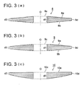
- FIGs. 3(a) to 3(c) show cross-sectional views that show a base plate used as a base material for a substrate for a magnetic information recording medium of a third embodiment according to the present invention.
- the surface of the resin base plate 2 is made flat and horizontal, and the thickness of the resin base plate 2 is uniform from its central portion to its circumferential portion; however in the third embodiment, the thickness of the central portion of the resin base plate is different from the thickness of the circumferential portion.
- a resin base plate 8 As shown in a cross-sectional view of FIG. 3(a), a resin base plate 8 according to a third embodiment has an aperture 8c which penetrates vertically at the central portion O of the base plate, and thickness of the base plate gradually decreases from the central portion O towards the circumferential portion 8d of the resin base plate 8. That is, the circumferential portion is thinner than the central portion O.
- surfaces 8a and 8b of the resin base plate 8 are made flat and inclined thereby making the substrate gradually thinner towards the circumferential portion 8d.
- the thickness of the central portion O is "thickness d1" and if the thickness of the circumferential portion 8d is "thickness d2,” the established relation is thickness d1 > thickness d2.
- This resin base plate 8 can also be made in the same manner as the first and second embodiments (injection molding, etc.). Moreover, the angle of inclination of the surfaces 8a and 8b can be flexibly determined by changing the shape of the die used for making the resin base plate 8. For example, given a base plate with an outside diameter of 1 inch, if the thickness d1 of the central portion O is 1 mm, the thickness of the circumferential portion 8d may be reduced down to 0.3 mm.
- a resin base plate is made by injection molding
- resin is filled from a gate provided at the central portion to form a substrate, and then an aperture is formed by removing an area located at the central portion, thereby creating a molded base plate.
- An inclination angle of the surface 8a may be identical to or different from the inclination angle of the surface 8b. Regardless of the inclination angles of two surfaces 8a and 8b, as long as the substrate is thick at the central portion O and gradually becomes thinner towards the circumferential portion 8d, the above operation and effects can be obtained.
- a resin base plate 9 as shown in FIG. 3(b) may be used as a resin base plate.
- a resin base plate 9 also has an aperture 9c which penetrates vertically at the central portion O of the base plate, and the thickness of the base plate gradually decreases from the central portion O towards the circumferential portion 9d of the resin base plate 9.
- surfaces 9a and 9b of the resin base plate 9 are convex curved surfaces, and by making the two surfaces 9a and 9 convex and curved, it is possible to make the substrate gradually thinner towards the circumferential portion 9d.
- a resin base plate 10 as shown in FIG. 3(c) may be used as a resin base plate.
- a resin base plate 10 also has an aperture 10c which penetrates vertically at the central portion O of the base plate, and the thickness of the base plate gradually decreases from the central portion O towards the circumferential portion 10d of the resin base plate 10.
- surfaces 10a and 10b of the resin base plate 10 are flat, but, the surface 10a is horizontal and the opposite surface 10b is inclined.
- Both sides of the resin base plate 8a are inclined; however, one side (surface 10a) of the resin base plate 10, shown in FIG. 3(c), is uniformly horizontal and only the other side (surface 10b) is inclined.
- one surface is made into an inclined plane (surface 10b), the thickness of the base plate gradually becomes thinner from the central portion O towards the circumferential portion 10d.
- a covering layer 3a and an intermediate layer 6a are formed on the resin base plate 10, they are formed on the horizontal surface 10a. Moreover, it is also possible to form a covering layer 3b and an intermediate layer 6b on the inclined surface 10b.
- resin base plate 8, 9 and 10 according to the third embodiment are different in shape from the resin base plate according to the first and second embodiments; however, material, surface roughness Ra, and arbitrarily included particles are the same as those in the first and second embodiments.
- a covering layer 6a is formed on the surfaces of the resin base plate 8, 9 and 10, shown in FIGs. 3(a), 3(b) and 3(c) respectively, in the same manner as the first embodiment, thereby making a substrate for a magnetic information recording medium. If surface roughness Ra of the covering layer 3a is not a desired value (for example, Ra ⁇ 1 nm), the surface of the covering layer 3a is ground and polished to have desired surface roughness Ra thereby creating a magnetic information recording medium substrate; then, a magnetic layer is formed on the covering layer 3a thereby creating a magnetic information recording medium.
- a desired value for example, Ra ⁇ 1 nm
- an intermediate layer 3a between the resin base plate 8, 9 and 10 and the covering layer 6a in the same manner as the second embodiment.
- Covering layers 6a and 6b and intermediate layers 6a and 6b may also be formed on both sides of the resin base plate 8, 9 and 10.
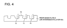
- particles formed of a material different from the surrounding material are included in the resin base plate or intermediate layer 6a (6b), and the surface of the resin base plate 2 or the intermediate layer 6a(6b) is dissolved by a solvent thereby making particles contained in the resin base plate 2 or the intermediate layer 6a(6b) exposed and thus purposely making the surface rough.
- etching the resin base plate 2 or the intermediate layer 6a(6b) to remove portions of or the entire particles included in the surface area it is possible to purposely make the surface rough.
- the rough shapes include deep concave shapes that were made by scooping out resin from the surface, adhesiveness may be further increased. For example, as shown in a cross-sectional view of FIG.
- the example 1 corresponds to the above first embodiment.
- a covering layer 3a is formed on the surface of one side of a resin base plate 2 to create a substrate for a magnetic information recording medium.
- a substrate for a magnetic information recording medium according to example 1 employs polyimide as a base material (resin base plate), and a resin base plate 2 is formed in a disc shape by the injection molding technique.
- polyimide As polyimide, AURUM (Mitsui Chemicals) was used.
- the dimensions of the resin base plate 2 are as follows:
- NiP layer an NiP alloy plated layer (hereafter, referred to as NiP layer) was formed on the Ni layer by further conducting the nonelectrolytic plating.
- the NiP layer is 30 ⁇ m thick.
- the Ni layer and the NiP layer constitute a covering layer 3a.
- the surface of the covering layer 3a was polished.
- Slurry that is mainly composed of colloidal silica was used as a polishing agent in this polishing process.
- Surface roughness Ra of the polished substrate for a magnetic information recording medium was 0.4 nm.
- a cobalt-base alloy magnetic layer was formed on the covering layer 3a by the sputtering operation, thereby creating a magnetic information recording medium.
- polyimide was used for a base material of the resin base plate 2 in this example 1; however, other different kinds of resin mentioned in the above first embodiment can be used to obtain the same effects as example 1.
- the covering layer 3a was an NiP layer, however, a layer that includes other components mentioned in the first embodiment can be used to obtain the same effects as example 1.
- the example 2 corresponds to the above second embodiment.
- an explanation will be given about an example in which an intermediate layer 6a is formed on the surface of one side of a resin base plate 2, and a covering layer 3a is then formed on the intermediate layer 6a thereby creating a substrate for a magnetic information recording medium.
- a substrate for a magnetic information recording medium according to example 2 employs cyclic polyolefin resin as a base material (resin base plate), and a resin base plate 2 is formed in a disc shape by the injection molding technique.
- cyclic polyolefin APEL (Mitsui Chemicals) was used.
- the dimensions of the resin base plate 2 are as follows:
- a covering layer 3a was formed on the intermediate layer 6a.
- the resin base plate 2 on which an intermediate layer 6a has been formed was etched.
- etching was conducted until portions of the particles contained in the intermediate layer 6a protrude from the surface.
- the intermediate layer 6a was removed by etching, and portions of the particles contained in the intermediate layer 6a protrude from the surface. Protruding particles cause rough shapes to be formed on the surface of the intermediate layer 6a.
- Ni layer was formed on the intermediate layer 6a by means of nonelectrolytic plating, and then an NiP layer was formed on the Ni layer by further conducting the nonelectrolytic plating.
- the NiP layer was 35 ⁇ m thick.
- a 5- ⁇ m thick Cr layer was formed on the NiP layer by the electrolytic plating.
- the Ni layer, NiP layer, and Cr layer constitute a covering layer 3a.
- portions of the particles contained in the intermediate layer 6a protrude from the surface; and the protruding particles cause level differences to be formed on the surface of the intermediate layer 6a thereby making the surface rough.
- surface of the intermediate layer 6a becomes rough, and therefore the plated Ni layer and NiP layer firmly adhere to the surface of the intermediate layer 6a. That is, by making the surface of the intermediate layer 6a rough as the result of the presence of the particles, it is possible to increase adhesiveness between the intermediate layer 6a and the covering layer 3a such as an NiP layer.
- forming a Cr layer on an NiP layer makes it possible to prevent the NiP layer from becoming cloudy.
- the surface of the covering layer 3a was polished.
- Slurry that is mainly composed of colloidal silica was used as a polishing agent in this polishing process.
- the surface roughness Ra of the polished substrate 1 for a magnetic information recording medium was 0.4 nm.
- a cobalt-base alloy magnetic layer is formed on the covering layer 3a by the sputtering operation, thereby creating a magnetic information recording medium.
- cyclic polyolefin resin was used for a base material of the resin base plate 2 in this example 2, however, other different kinds of resin mentioned in the above first embodiment can be used to obtain the same effects as example 2.
- ultraviolet-curable acrylic resin was used for an intermediate layer 6a; however, other different kinds of resin mentioned in the above second embodiment can be used to obtain the same effects as example 2.
- the covering layer 3a comprised an NiP layer and a Cr layer, however, a layer that includes other components mentioned in the first embodiment can be used to obtain the same effects as example 2.
- the example 3 corresponds to the above third embodiment.
- a specific example of the resin base plate 9 shown in FIG. 3(b) will be explained.
- the dimensions of the resin base plate 9 according to example 3 are as follows:
- a covering layer 3a was formed on the resin base plate 9 which has been created as stated above, and its surface was polished thereby creating a final substrate for a magnetic information recording medium.
- the thickness of the covering layer 3a before and after the polishing process is the same as that of the above example 1.
- an intermediate layer 6a was formed on the resin base plate 9, and a covering layer 3a was formed on the intermediate layer 6a; subsequently, the surface of the covering layer 3a was polished thereby creating a final substrate for a magnetic information recording medium.
- the thickness of the intermediate layer 6a is the same as that of the above example 2.
- a cobalt-base alloy magnetic layer was formed on the covering layer 3a by the sputtering operation, thereby creating a magnetic information recording medium.
- example 3 it is possible to reduce wobbling caused by the rotation of a magnetic information recording medium, thereby increasing the tracking performance of the magnetic head. Furthermore, because the central portion of the base plate is made thicker than the circumferential portion, it was verified that fluidity of resin is increased and the molding process is made easy when a resin base plate 9 is made by injection molding.
- curvature radius R of surfaces 9a and 9b depends on the dimensions of the base plate, for example, when the size of the base plate is 1 inch, it is preferable that the curvature radius R be 135 mm or more.
Landscapes
- Engineering & Computer Science (AREA)
- Manufacturing & Machinery (AREA)
- Magnetic Record Carriers (AREA)
- Manufacturing Of Magnetic Record Carriers (AREA)
Applications Claiming Priority (1)
| Application Number | Priority Date | Filing Date | Title |
|---|---|---|---|
| JP2005249878A JP2007066390A (ja) | 2005-08-30 | 2005-08-30 | 磁気記録媒体用基板、及び磁気記録媒体用基板の製造方法 |
Publications (1)
| Publication Number | Publication Date |
|---|---|
| EP1760699A1 true EP1760699A1 (de) | 2007-03-07 |
Family
ID=37074599
Family Applications (1)
| Application Number | Title | Priority Date | Filing Date |
|---|---|---|---|
| EP06254457A Withdrawn EP1760699A1 (de) | 2005-08-30 | 2006-08-25 | Substrat für ein magnetisches Informationsaufzeichnungsmedium und Verfahren zur Substratherstellung für ein magnetisches Informationsaufzeichnungsmedium |
Country Status (6)
| Country | Link |
|---|---|
| US (1) | US20070048553A1 (de) |
| EP (1) | EP1760699A1 (de) |
| JP (1) | JP2007066390A (de) |
| KR (1) | KR20070026038A (de) |
| CN (1) | CN1925012A (de) |
| TW (1) | TW200729176A (de) |
Families Citing this family (10)
| Publication number | Priority date | Publication date | Assignee | Title |
|---|---|---|---|---|
| DE102005034627A1 (de) * | 2005-07-19 | 2007-02-01 | Takata-Petri Ag | Vorrichtung und Verfahren zum Entfernen eines längs erstreckten Grates an einem Formteil |
| WO2007119306A1 (ja) * | 2006-03-13 | 2007-10-25 | Konica Minolta Opto, Inc. | 磁気記録媒体用基板、その製造方法、及び磁気記録媒体 |
| JP4539723B2 (ja) * | 2008-01-21 | 2010-09-08 | Dic株式会社 | 熱転写用積層体およびこれを用いた磁気記録媒体の製造方法 |
| WO2010001844A1 (ja) * | 2008-06-30 | 2010-01-07 | Hoya株式会社 | 磁気ディスク用基板及びその製造方法並びに磁気ディスク |
| CN102964140B (zh) * | 2011-08-31 | 2014-09-03 | 深圳光启高等理工研究院 | 一种超材料介质基板的制备方法 |
| WO2013047189A1 (ja) * | 2011-09-30 | 2013-04-04 | コニカミノルタアドバンストレイヤー株式会社 | 情報記録媒体用ガラス基板および情報記録媒体 |
| US9224412B2 (en) * | 2014-01-31 | 2015-12-29 | HGST Netherlands B.V. | Perpendicular magnetic recording disk with template layer formed of a blend of nanoparticles |
| JP5863206B2 (ja) * | 2014-06-09 | 2016-02-16 | 東芝エレベータ株式会社 | エレベータ群管理装置 |
| PH12021552252A1 (en) * | 2017-03-31 | 2022-05-02 | Hoya Corp | Non-magnetic substrate for magnetic disk, and magnetic disk |
| WO2019004484A1 (ja) | 2017-06-30 | 2019-01-03 | Hoya株式会社 | 磁気ディスク用基板及び磁気ディスク |
Citations (22)
| Publication number | Priority date | Publication date | Assignee | Title |
|---|---|---|---|---|
| JPS61236021A (ja) * | 1985-04-10 | 1986-10-21 | Diafoil Co Ltd | 磁気デイスク用3−メチルブテン−1重合体フイルム |
| US4654741A (en) * | 1984-09-28 | 1987-03-31 | Kabushiki Kaisha Toshiba | Magnetic disc apparatus with liner that avoids bent edges of magnetic discs |
| JPS63268122A (ja) * | 1987-04-24 | 1988-11-04 | Matsushita Electric Works Ltd | 磁気デイスク基板 |
| JPS63268123A (ja) * | 1987-04-24 | 1988-11-04 | Matsushita Electric Works Ltd | 磁気デイスク基板 |
| JPH01106334A (ja) * | 1987-10-19 | 1989-04-24 | Toa Nenryo Kogyo Kk | 磁気ディスク用支持体およびその製造方法 |
| JPH01302530A (ja) * | 1988-05-30 | 1989-12-06 | Tonen Corp | 磁気ディスク用基体およびその製造法 |
| JPH02161609A (ja) * | 1988-12-13 | 1990-06-21 | Sekisui Chem Co Ltd | 磁気記録媒体 |
| JPH02208819A (ja) * | 1989-02-08 | 1990-08-20 | Sekisui Chem Co Ltd | 磁気記録媒体 |
| JPH02252120A (ja) * | 1989-03-27 | 1990-10-09 | Nissei Plastics Ind Co | 記録ディスク用基盤 |
| JPH035918A (ja) * | 1989-05-31 | 1991-01-11 | Sekisui Chem Co Ltd | 磁気記録媒体用基板 |
| JPH0388118A (ja) * | 1989-08-31 | 1991-04-12 | Toray Ind Inc | 磁気記録媒体 |
| JPH04143920A (ja) * | 1990-10-03 | 1992-05-18 | Tdk Corp | 磁気ディスク |
| US5119259A (en) * | 1989-12-06 | 1992-06-02 | Fuji Photo Film Co., Ltd. | Magnetic disk |
| EP0655734A1 (de) * | 1993-11-30 | 1995-05-31 | Sony Corporation | Magnetplattensubstrat und Magnetplatte welche dieses verwendet |
| JPH0991690A (ja) * | 1995-09-22 | 1997-04-04 | Sony Corp | 磁気ディスク及びディスクドライブ装置 |
| JPH10134334A (ja) * | 1996-09-03 | 1998-05-22 | Hitachi Ltd | 磁気ディスク及びそれを用いた磁気記録装置 |
| JPH11306534A (ja) * | 1998-04-23 | 1999-11-05 | Sony Corp | 磁気記録媒体 |
| JPH11353649A (ja) * | 1998-06-12 | 1999-12-24 | Sony Corp | 樹脂製情報記録媒体の製造方法及び製造用スペーサ |
| DE10032565A1 (de) * | 1999-07-07 | 2001-01-11 | Fuji Electric Co Ltd | Magnetscheibensubstrat, Magnetaufzeichnungsmedium und Verfahren zum Herstellen eines Magnetscheibensubstrats |
| US20030035980A1 (en) * | 2001-05-09 | 2003-02-20 | Takahiro Igari | Magnetic recording medium |
| EP1316947A1 (de) * | 2000-09-04 | 2003-06-04 | Zeon Corporation | Magnetplattensubstrat und magnetplatte |
| US20040151948A1 (en) * | 2002-11-14 | 2004-08-05 | Youichi Tei | Magnetic recording medium substrate using thermoplastic allyloxymethylstyrene resin, magnetic recording medium using the substrate, and method of manufacturing the magnetic recording medium |
Family Cites Families (16)
| Publication number | Priority date | Publication date | Assignee | Title |
|---|---|---|---|---|
| JPS61187117A (ja) * | 1985-02-15 | 1986-08-20 | Ayao Wada | 磁気デイスク用基板 |
| JPS6248015U (de) * | 1985-09-13 | 1987-03-25 | ||
| JPS6488916A (en) * | 1987-09-29 | 1989-04-03 | Kobe Steel Ltd | Composite substrate for magnetic disk |
| JPH02130718A (ja) * | 1988-11-09 | 1990-05-18 | Sekisui Chem Co Ltd | 磁気記録媒体 |
| US6066380A (en) * | 1996-08-23 | 2000-05-23 | Sony Corporation | Disc medium substrate and disc device |
| JP3509838B2 (ja) * | 1996-12-16 | 2004-03-22 | 戸田工業株式会社 | 鉄を主成分とする金属磁性粒子粉末を使用している磁気記録媒体の非磁性下地層用酸化チタン粒子粉末、該酸化チタン粒子粉末を用いた非磁性下地層を有する磁気記録媒体の基体並びに該基体を用いた磁気記録媒体 |
| EP0853066B1 (de) * | 1997-01-08 | 2000-10-04 | Toda Kogyo Corp. | Hematitteilchen und magnetischer Aufzeichnungsträger welcher die Hematitteilchen als nicht-magnitische Teilchen in einer nicht-magnetischen Unterschicht verwendet |
| JP3514068B2 (ja) * | 1997-03-27 | 2004-03-31 | 戸田工業株式会社 | 磁気記録媒体の非磁性下地層用ヘマタイト粒子粉末及びその製造法、磁気記録媒体の非磁性下地層及び磁気記録媒体 |
| JPH10334445A (ja) * | 1997-06-02 | 1998-12-18 | Kobe Steel Ltd | 磁気ディスク用基板 |
| US6159592A (en) * | 1997-11-28 | 2000-12-12 | Toda Kogyo Corporation | Magnetic recording medium |
| US6764734B2 (en) * | 1998-05-19 | 2004-07-20 | Seagate Technology Llc | High modulus and high damping plastic composite disc substrate for improved servo control by injection and co-injection molding |
| JPH11345412A (ja) * | 1998-05-29 | 1999-12-14 | Sony Corp | 記録媒体用基板及び記録媒体 |
| WO2000048172A2 (en) * | 1999-02-12 | 2000-08-17 | General Electric Company | Data storage media |
| US6974642B2 (en) * | 2000-03-15 | 2005-12-13 | Fujitsu Limited | Carbonaceous protective layer, magnetic recording medium, production method thereof, and magnetic disk apparatus |
| US6767584B2 (en) * | 2002-05-13 | 2004-07-27 | International Business Machines Corporation | Disk substrate with monosized microbumps |
| JP2005092991A (ja) * | 2003-09-18 | 2005-04-07 | Fuji Photo Film Co Ltd | 磁気記録媒体 |
-
2005
- 2005-08-30 JP JP2005249878A patent/JP2007066390A/ja active Pending
-
2006
- 2006-08-25 US US11/509,772 patent/US20070048553A1/en not_active Abandoned
- 2006-08-25 KR KR1020060080832A patent/KR20070026038A/ko not_active Withdrawn
- 2006-08-25 CN CNA2006101262172A patent/CN1925012A/zh active Pending
- 2006-08-25 EP EP06254457A patent/EP1760699A1/de not_active Withdrawn
- 2006-08-28 TW TW095131676A patent/TW200729176A/zh unknown
Patent Citations (23)
| Publication number | Priority date | Publication date | Assignee | Title |
|---|---|---|---|---|
| US4654741A (en) * | 1984-09-28 | 1987-03-31 | Kabushiki Kaisha Toshiba | Magnetic disc apparatus with liner that avoids bent edges of magnetic discs |
| JPS61236021A (ja) * | 1985-04-10 | 1986-10-21 | Diafoil Co Ltd | 磁気デイスク用3−メチルブテン−1重合体フイルム |
| JPS63268122A (ja) * | 1987-04-24 | 1988-11-04 | Matsushita Electric Works Ltd | 磁気デイスク基板 |
| JPS63268123A (ja) * | 1987-04-24 | 1988-11-04 | Matsushita Electric Works Ltd | 磁気デイスク基板 |
| JPH01106334A (ja) * | 1987-10-19 | 1989-04-24 | Toa Nenryo Kogyo Kk | 磁気ディスク用支持体およびその製造方法 |
| JPH01302530A (ja) * | 1988-05-30 | 1989-12-06 | Tonen Corp | 磁気ディスク用基体およびその製造法 |
| JPH02161609A (ja) * | 1988-12-13 | 1990-06-21 | Sekisui Chem Co Ltd | 磁気記録媒体 |
| JPH02208819A (ja) * | 1989-02-08 | 1990-08-20 | Sekisui Chem Co Ltd | 磁気記録媒体 |
| JPH02252120A (ja) * | 1989-03-27 | 1990-10-09 | Nissei Plastics Ind Co | 記録ディスク用基盤 |
| JPH035918A (ja) * | 1989-05-31 | 1991-01-11 | Sekisui Chem Co Ltd | 磁気記録媒体用基板 |
| JPH0388118A (ja) * | 1989-08-31 | 1991-04-12 | Toray Ind Inc | 磁気記録媒体 |
| US5119259A (en) * | 1989-12-06 | 1992-06-02 | Fuji Photo Film Co., Ltd. | Magnetic disk |
| JPH04143920A (ja) * | 1990-10-03 | 1992-05-18 | Tdk Corp | 磁気ディスク |
| EP0655734A1 (de) * | 1993-11-30 | 1995-05-31 | Sony Corporation | Magnetplattensubstrat und Magnetplatte welche dieses verwendet |
| EP1001408A2 (de) * | 1993-11-30 | 2000-05-17 | Sony Corporation | Magnetplattensubstrat und Magnetplatte welche dieses verwendet |
| JPH0991690A (ja) * | 1995-09-22 | 1997-04-04 | Sony Corp | 磁気ディスク及びディスクドライブ装置 |
| JPH10134334A (ja) * | 1996-09-03 | 1998-05-22 | Hitachi Ltd | 磁気ディスク及びそれを用いた磁気記録装置 |
| JPH11306534A (ja) * | 1998-04-23 | 1999-11-05 | Sony Corp | 磁気記録媒体 |
| JPH11353649A (ja) * | 1998-06-12 | 1999-12-24 | Sony Corp | 樹脂製情報記録媒体の製造方法及び製造用スペーサ |
| DE10032565A1 (de) * | 1999-07-07 | 2001-01-11 | Fuji Electric Co Ltd | Magnetscheibensubstrat, Magnetaufzeichnungsmedium und Verfahren zum Herstellen eines Magnetscheibensubstrats |
| EP1316947A1 (de) * | 2000-09-04 | 2003-06-04 | Zeon Corporation | Magnetplattensubstrat und magnetplatte |
| US20030035980A1 (en) * | 2001-05-09 | 2003-02-20 | Takahiro Igari | Magnetic recording medium |
| US20040151948A1 (en) * | 2002-11-14 | 2004-08-05 | Youichi Tei | Magnetic recording medium substrate using thermoplastic allyloxymethylstyrene resin, magnetic recording medium using the substrate, and method of manufacturing the magnetic recording medium |
Also Published As
| Publication number | Publication date |
|---|---|
| CN1925012A (zh) | 2007-03-07 |
| US20070048553A1 (en) | 2007-03-01 |
| JP2007066390A (ja) | 2007-03-15 |
| KR20070026038A (ko) | 2007-03-08 |
| TW200729176A (en) | 2007-08-01 |
Similar Documents
| Publication | Publication Date | Title |
|---|---|---|
| EP1760699A1 (de) | Substrat für ein magnetisches Informationsaufzeichnungsmedium und Verfahren zur Substratherstellung für ein magnetisches Informationsaufzeichnungsmedium | |
| JP2005196953A (ja) | Cd及びdvdにパターンを作成するためのスタンパを製造する方法及び装置 | |
| JP2002050031A (ja) | 多層テクスチャー層 | |
| CN115938404A (zh) | 具有高内应力以减小由冲击力引起的盘偏转的磁记录盘和用于与盘一起使用的方法 | |
| US8021713B2 (en) | Bit-patterned magnetic media formed in filler layer recesses | |
| US6314764B1 (en) | Method of manufacturing a 1-inch diameter glass substrate for a magnetic disk | |
| US6314763B1 (en) | Method of manufacturing a 2-5 inch diameter glass substrate for a magnetic disk | |
| EP2028652A1 (de) | Magnetisches Aufzeichnungsmedium und sein Herstellungsverfahren | |
| EP2006842A1 (de) | Verfahren zur Herstellung eines magnetischen Aufzeichnungsmediums, damit hergestelltes magnetisches Aufzeichnungsmedium und Formstruktur zur Verwendung für dieses Verfahren | |
| US12377514B2 (en) | Carrier and method for manufacturing substrate | |
| JP2004171658A (ja) | 垂直磁気記録媒体用基板および垂直磁気記録媒体並びにそれらの製造方法 | |
| US20050271799A1 (en) | Method for producing magnetic recording medium | |
| JP4892080B2 (ja) | スタンパの製造方法 | |
| JPWO2007119306A1 (ja) | 磁気記録媒体用基板、その製造方法、及び磁気記録媒体 | |
| CN1118915A (zh) | 制造磁头的方法 | |
| JP5062167B2 (ja) | 磁気記録媒体用基板 | |
| EP2009624A1 (de) | Verfahren zur Herstellung eines magnetischen Aufzeichnungsmediums, magnetisches Aufzeichnungsmedium, das mit dem Herstellungsverfahren hergestellt wurde, und Formstruktur zur Verwendung im Herstellungsverfahren | |
| US7757247B2 (en) | Small form factor optical/magnetic disk for information storage | |
| JPH05334666A (ja) | 磁気ディスクの製造方法および磁気ディスク | |
| JPH05334667A (ja) | 磁気ディスクの製造方法および磁気ディスク | |
| JP2009054252A (ja) | 磁気記録媒体用基板、磁気記録媒体、及び磁気記録装置 | |
| JP2009054253A (ja) | 磁気記録媒体用基板及び磁気記録装置 | |
| JP2009223999A (ja) | 金型部材、射出成形用金型、及び、磁気記録媒体用基板の製造方法 | |
| US20050166218A1 (en) | Magneto-optical recording medium and method for producing the same | |
| JP2006313617A (ja) | 光ディスク基板成膜装置、光ディスク基板成膜方法、基板ホルダーの製造方法、基板ホルダー、光ディスクおよび相変化記録型光ディスク |
Legal Events
| Date | Code | Title | Description |
|---|---|---|---|
| PUAI | Public reference made under article 153(3) epc to a published international application that has entered the european phase |
Free format text: ORIGINAL CODE: 0009012 |
|
| AK | Designated contracting states |
Kind code of ref document: A1 Designated state(s): AT BE BG CH CY CZ DE DK EE ES FI FR GB GR HU IE IS IT LI LT LU LV MC NL PL PT RO SE SI SK TR |
|
| AX | Request for extension of the european patent |
Extension state: AL BA HR MK YU |
|
| 17P | Request for examination filed |
Effective date: 20070807 |
|
| AKX | Designation fees paid |
Designated state(s): AT BE BG CH CY CZ DE DK EE ES FI FR GB GR HU IE IS IT LI LT LU LV MC NL PL PT RO SE SI SK TR |
|
| 17Q | First examination report despatched |
Effective date: 20071108 |
|
| STAA | Information on the status of an ep patent application or granted ep patent |
Free format text: STATUS: THE APPLICATION IS DEEMED TO BE WITHDRAWN |
|
| 18D | Application deemed to be withdrawn |
Effective date: 20080729 |