EP1723460B1 - Scanneur de systemes microelectromecaniques concu pour imprimante laser - Google Patents
Scanneur de systemes microelectromecaniques concu pour imprimante laser Download PDFInfo
- Publication number
- EP1723460B1 EP1723460B1 EP05713179.9A EP05713179A EP1723460B1 EP 1723460 B1 EP1723460 B1 EP 1723460B1 EP 05713179 A EP05713179 A EP 05713179A EP 1723460 B1 EP1723460 B1 EP 1723460B1
- Authority
- EP
- European Patent Office
- Prior art keywords
- mems scanner
- laser printer
- dimension
- scan plate
- torsion arms
- Prior art date
- Legal status (The legal status is an assumption and is not a legal conclusion. Google has not performed a legal analysis and makes no representation as to the accuracy of the status listed.)
- Not-in-force
Links
Images


Classifications
-
- G—PHYSICS
- G02—OPTICS
- G02B—OPTICAL ELEMENTS, SYSTEMS OR APPARATUS
- G02B26/00—Optical devices or arrangements for the control of light using movable or deformable optical elements
- G02B26/08—Optical devices or arrangements for the control of light using movable or deformable optical elements for controlling the direction of light
- G02B26/0816—Optical devices or arrangements for the control of light using movable or deformable optical elements for controlling the direction of light by means of one or more reflecting elements
- G02B26/0833—Optical devices or arrangements for the control of light using movable or deformable optical elements for controlling the direction of light by means of one or more reflecting elements the reflecting element being a micromechanical device, e.g. a MEMS mirror, DMD
- G02B26/0858—Optical devices or arrangements for the control of light using movable or deformable optical elements for controlling the direction of light by means of one or more reflecting elements the reflecting element being a micromechanical device, e.g. a MEMS mirror, DMD the reflecting means being moved or deformed by piezoelectric means
-
- G—PHYSICS
- G02—OPTICS
- G02B—OPTICAL ELEMENTS, SYSTEMS OR APPARATUS
- G02B26/00—Optical devices or arrangements for the control of light using movable or deformable optical elements
- G02B26/08—Optical devices or arrangements for the control of light using movable or deformable optical elements for controlling the direction of light
- G02B26/10—Scanning systems
- G02B26/105—Scanning systems with one or more pivoting mirrors or galvano-mirrors
-
- H—ELECTRICITY
- H04—ELECTRIC COMMUNICATION TECHNIQUE
- H04N—PICTORIAL COMMUNICATION, e.g. TELEVISION
- H04N1/00—Scanning, transmission or reproduction of documents or the like, e.g. facsimile transmission; Details thereof
- H04N1/04—Scanning arrangements, i.e. arrangements for the displacement of active reading or reproducing elements relative to the original or reproducing medium, or vice versa
- H04N1/113—Scanning arrangements, i.e. arrangements for the displacement of active reading or reproducing elements relative to the original or reproducing medium, or vice versa using oscillating or rotating mirrors
-
- H—ELECTRICITY
- H04—ELECTRIC COMMUNICATION TECHNIQUE
- H04N—PICTORIAL COMMUNICATION, e.g. TELEVISION
- H04N1/00—Scanning, transmission or reproduction of documents or the like, e.g. facsimile transmission; Details thereof
- H04N1/04—Scanning arrangements, i.e. arrangements for the displacement of active reading or reproducing elements relative to the original or reproducing medium, or vice versa
- H04N1/12—Scanning arrangements, i.e. arrangements for the displacement of active reading or reproducing elements relative to the original or reproducing medium, or vice versa using the sheet-feed movement or the medium-advance or the drum-rotation movement as the slow scanning component, e.g. arrangements for the main-scanning
- H04N1/121—Feeding arrangements
- H04N1/1235—Feeding a sheet past a transparent plate; Details thereof
- H04N1/124—Plate shape
Definitions
- the present invention relates to microelectromechanical system (MEMS) scanners and particularly to their application to laser printers.
- MEMS microelectromechanical system
- Electrophotographic, computer controlled printers have become pervasive in the office, factory, print shop, copy center, and home.
- An electrophotographic printer operates by transferring toner to plain paper and fusing the toner by means of heat, pressure, and/or other fixing technologies.
- the pattern of the transferred toner may form characters, graphic images, etc.
- electrophotography refers to the use of modulated light, frequently a scanned laser beam, to create an electrostatic latent image on a photoconductive carrying medium such as a drum or belt.
- the latent electrostatic image is formed by momentary electrical conductivity of the photoconductor in response to exposure to the modulated light.
- the momentary conductivity allows a surface charge to discharge through the photoconductor to a conductor held at a bias voltage at locations corresponding to the modulated light exposure.
- FIG. 1 is a diagram illustrating the principal features of an electrophotographic printer.
- a photoconductive drum 102 is rotated past a charging or sensitization station 104 that deposits a static charge substantially uniformly over the surface of the drum 102.
- An imaging module 106 modulate light selectively over the surface of the photoconductor 102. This causes the static charge in those spots receiving light to discharge through the photoconductive layer to a conductive layer on the backside of the photoconductor surface.
- the pattern of discharged and non-discharged spots is referred to as a latent electrostatic image or latent image.
- Electrophotographic printers may be made to write-white or write-black.
- the toner charge is selected to be attracted to the photoconductor backside conductive layer bias voltage and repelled from the sensitization static charge deposited on the photoconductor surface.
- the spots "written" by the modulated light correspond to black areas of the printed page.
- the photoconductor 102 is further rotated to a developer 108, where oppositely charged toner, most often in the form of fine, dry particles, is attracted to and deposited on the surface of the photoconductor in a pattern corresponding to the latent image.
- the photoconductor 102 is further rotated to a transfer point, where the patterned toner is then transferred to the paper 112, often using an electrostatic attraction element 110 such as a corona wire in the form of a corotron or scorotron.
- the paper 112 with toner loosely adhered thereto, is fed forward through a fusing station 114 that, generally through a combination of heat and pressure, causes the thermoplastic toner particles to permanently adhere to the paper, thus forming a robust image.
- the photoconductive medium 102 is rotated past a discharge lamp 116 and a cleaner 118, and then repeats the process as it is rotated to the sensitizer or charger 104.
- LED light emitting diode
- LCD liquid crystal shutter
- vacuum fluorescent vacuum fluorescent
- other types of arrayed light modulator write heads have been used for modulating light onto the photoconductor.
- scanned laser beam exposure or imaging modules have gained favor in the art due to an appropriate balance of cost, speed, performance, and durability.
- An electrophotographic printer that uses a scanned laser beam to provide light modulation onto the surface of the photoconductive medium may be conveniently referred to as a laser beam printer or LBP.
- FIG. 2 illustrates the general construction of an LBP exposure unit 106 made according to the prior art with a rotating polygon beam scanner.
- a laser diode 202 having a wavelength matched to the sensitivity of the photoconductor (often infrared in the case or an organic photoconductor) is modulated with an image Signal.
- Beam-forming optics 204 produce a laser beam having a desired shape and trajectory.
- the laser beam is reflected off a rotating polygon mirror 206 and is scanned across the photoconductor 102 through optical elements 208.
- the design or the exposure module 106 is such that the reflective facets 210a, 210b, etc. of the rotating polygon 206 are placed forward of the center of rotation such that the arriving beam sweeps over each mirror surface as it is deflected across its deflection angle, the deflection angle being sufficient to traverse the photoconductor 102.
- Rotating polygon mirrors may suffer from relatively large mass, slow ramp-up to speed, large size, noise, bearing reliability issues, relatively high power consumption, and other shortcomings.
- U.S. Patent Application 2003/072066 A1 discloses an optical scanning device comprising a plurality of scanning optical systems including a plurality of respective deflecting units each performing an optical scanning by oscillation, wherein the deflecting units have substantially equal scanning frequencies.
- the scanning device has a scan plate, two torsion arms defining an axis of rotation of the scan plate and two opposed mounting stmctures.
- U.S. Patent No. 6,360,035 discloses a MEMS-based optical microswitch for use with a laser beam comprising a support body and first and second output fibers carried by the body.
- U.S. Patent Application 2003/0053156 A1 discloses an optical scanning device comprising an optical deflector with a movable mirror and torsion bars supporting the mirror and formed integrally with the mirror.
- U.S. Patent No. 6,672,732 discloses a micromechanical oscillating device comprising a vibrating structure which is connected to a supporting body via a spring structure.
- the spring structure comprises a torsion-spring element, which defines a torsion axis and permits a torsional vibration about the torsion axis, and a converter structure, which partially converts forces acting perpendicularly to the torsion axis into forces acting in a parallel manner to the torsion axis.
- MEMS microelectromechanical system
- a MEMS laser beam scanner may be formed with various physical and operational attributes; including mirror size, scan angle, scan frequency, and mirror flatness; to be especially well-adapted to an electrophotographic printer exposure unit.
- a MEMS mirror with extended length transverse the scanning axis can be substituted for a rotating polygon without substantial modifications to the exposure module optical design.
- FIG. 3 illustrates a MEMS scanner 302 that may be used in a LBP.
- the exemplary embodiment shown herein relates to a 40 page per minute (ppm), 1200 dot per inch (dpi) LBP.
- MEMS scanner 302 is photolithographically formed from single-crystal silicon using bulk micromachining as is known to the art.
- a scan plate 304 having a mirror surface is coupled to a pair of torsion arms 306a, 306b through respective suspension beams 308a, 308b.
- Torsion arms 306a, 306b define a rotational axis 310 about which scan plate 304 and suspension beams 308a, 308b rotate.
- Suspension beams 308a and 308b help to keep the mirror surface relatively flat, typically within lambda/4, by spreading the torque loads induced by the torsion arms 306a, 306b across the surface of the scan plate 304.
- Suspension beams 308 are coupled to scan plate 304 by respective outer (lateral) connectors 316a, 316b, 316c, 316d and respective axial connectors 318a, 318b. Taken together, suspension elements 308a, 316a, 316b, and 318a form a first suspension coupling between first torsion arm 306a and scan plate 304. Similarly suspension elements 308b, 316c, 316d, and 318b form a second suspension coupling between second torsion arm 306b and scan plate 304.
- a mirror surface can be formed on the surface of scan plate 304 using metal, stacked dielectric, or other technologies known to the art.
- Aluminum can be used to form a mirror having greater than about 85% reflectivity at red and infrared wavelengths (having a local minimum at about 825 nanometers wavelength).
- Gold or silver can be used to form a mirror having greater than about 90% to 95% reflectivity at red and infrared wavelengths.
- Stacked (such as quarter-wave) dielectric reflectors can achieve very high reflectivity across a wide range of wavelengths.
- Torsion arms 306a, 306b terminate at respective "T-bars" 312a and 312b.
- T-bars 312a and 312b connect to respective mounting pads 314a, 314b and 314c, 314d as illustrated.
- T-bar 312a and mounting pads 314a, 314b constitute a first mounting structure for coupling torsion arm 306a to a support structure (not shown).
- T-bar 312b and mounting pads 314c, 314d form a second mounting structure for coupling torsion arm 306b to a support structure (not shown).
- mounting structures can take other forms, including for example a pair of rectangular mounting pads, each joined directly to a respective torsion arm, or other forms.
- a frame-type mounting structure may be formed peripheral to the scan plate 304 and torsion arms 306a, 306b.
- the exemplary embodiment of Figure 3 may have certain advantages such as, for example, packing more devices per wafer, having reduced dynamic stress, allowing individual mounting pads to be coupled to actuators, and allowing the mounting pads 314 to "float" relative to one another, thereby reducing residual stresses in the MEMS scanner.
- Scan plate 304 is formed to be approximately 8 millimeters long (in the direction perpendicular to the axis of rotation 310) and 750 micrometers wide (in the direction parallel to the axis of rotation 310).
- the scan plate (and mirror formed thereon) has a lateral dimension about 10.67 times its longitudinal dimension.
- the mirror When driven with an appropriate signal, (such as a 5 kilohertz (KHz) sine wave varying between about 0 (zero) and 25-30 volts for a four actuator design) the mirror responds with a ⁇ 20° mechanical scan angle at a frequency of 5 KHz.
- KHz kilohertz
- MEMS scanner 302 includes two torsion arms 306a, 306b, each 8.76 millimeters long (including fillets), terminated on their proximal ends by a 400 micrometer by 200 micrometer elliptical fillet at respective suspensions (in particular at suspension beams 308a, 308b), and terminated on their distal ends at respective T-bars 312a, 312b, again with a 400 micrometer by 200 micrometer elliptical fillet.
- the torsion arms 306a, 306b are 384 micrometers wide. As with the rest of MEMS scanner 302, the torsion arms are etched to a full wafer thickness of 700 micrometers using DRIE processing. For a given scan plate mass and mass distribution, the width, depth, and length of the torsion arms and T-bars may be adjusted to produce alternative resonant scan frequencies and angles.
- the suspension beams 308a, 308b are 396 micrometers wide, are slightly bent to make a slightly obtuse angle with respective torsion arms 306a, 306b of 91.6 degrees, and extend laterally to an extent equal to the lateral extent of the 8 millimeter lateral dimension scan plate 304.
- Respective suspension center connectors 318a, 318b extend from the centerlines of suspension beams 308a, 308b to the centerline of the scan plate 304, a distance of 500 micrometers (including fillets).
- the center connectors 318a, 318b are each 164 micrometers wide and include 100 micrometers radius fillets at both ends.
- suspension outer connectors 316a, 316b, 316c, and 316d extend from the ends of suspension beams 308a, 308b to the scan plate 304, one on each end of each suspension beam as indicated.
- the outer connectors 316a, 316b, 316c, 316d are each 250 micrometers wide (laterally) by 400 micrometers long (longitudinally) and do not have fillets.
- the respective suspensions thus each include a suspension beam 308, a center suspension connector 318, and two outer suspension connectors 316; and connect the torsion arms 306a, 306b to the scan plate 304 in a manner that reduces stress concentrations, spreads the torque load, and reduces dynamic deformation of the scan plate during operation.
- Alternative suspension configurations are possible and could be implemented by one skilled in the art.
- the T-bars 312a, 312b are each 1.8 millimeters long (total lateral dimension inclusive of fillets) by 400 micrometers wide (longitudinal dimension) and extend symmetrically from and perpendicular to the axis formed by torsion arms 306a, 306b.
- the outer ends of T-bars 312a, 312b connect to four respective mounting pads 314a, 314b, 314c, 314d with 200 micrometer radius fillets as shown.
- the mounting pads are each 5 millimeters square. The geometry of the T-bars and mounting pads may be adjusted to suit application requirements.
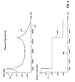
- Figure 4 shows graphs illustrating the dynamic response of the MEMS scanner of Figure 3 when a periodic drive signal is applied.
- Curve 402 indicates an amplitude response 404 as a function of periodic drive frequency 406.
- Curve 408 illustrates scanner vs. drive phase 410 plotted against the same periodic drive frequency axis 406. From inspection of curve 402, one can see a peak in response at about 5 KHz corresponding to the resonance frequency of the MEMS scanner in the rotation mode. While the size of the peak is plotted on a relative basis, it is, for the exemplary embodiment, sufficiently high to produce a resonance response of ⁇ 20° mechanical scan angle at acceptable drive power.
- a drive waveform approximating a 5 KHz sine wave with amplitude of 0 (zero) to 25-30 volts results in ⁇ 20° mechanical scan angle.
- the secondary peak at between 65 and 70 KHz corresponds to the resonant behavior of the piezo-electric stack actuators.
- Curve 408 illustrates how the phase relationship of the drive signal to the MEMS scanner response inverts at the resonance points. Below 5 KHz, the phase relationship (drive to response) is 0°. Above 5 KHz but below the secondary peak, the phase relationship is -180°. At the primary resonant peak, the phase relationship inverts and passes through -90° (response lagging drive) as indicated. Above the secondary peak, the response of the system drops and the phase response again inverts, passing from -180° below the peak, through -270°(+90°) at the secondary resonance peak, to -360° (0°) at frequencies above the secondary resonance peak. To maximize efficiency, it has been found to be advantageous to operate the MEMS scanner at or very near the primary resonance peak.
- the resonance frequency of the MEMS scanner is trimmed to be a few hertz above 5 KHz, typically in the range of 5.001 to 5.005 KHz. Such trimming may be accomplished using methods described in U.S. Patent Number 6,245,590 . It has been found to be advantageous to factory trim resonant frequency using a method of adding weight, in the form of epoxy applied to the scan plate.
- FIG. 5 illustrates a prototypical layout of MEMS scanners 302a, 302b, 302c, 302d, 302e, and 302f on a 100 millimeter silicon wafer 502.
- the MEMS scanners are densely packed with interdigitated mounting pads and mirrors. This is done to maximize yield per wafer. Larger wafers would be similarly densely packed with devices. Rather than dicing the devices apart using a dicing saw, a photolithographic step such as deep reactive ion etch (DRIE) is used to almost completely release the scanners from the wafer. Very fine silicon “bridges" may be seen connecting the scanners to the wafer at intervals. To release the scanners, these bridges are simply broken and the scanners popped out.
- DRIE deep reactive ion etch
- Figure 5 further illustrates an alternate T-bar 312 design wherein the ends of the "T" are offset toward the scan plate. This can result in shorter part length or better interdigitation of neighboring parts on the wafer, and may be useful for minimizing scanner size, maximizing yield from the wafer, etc.
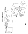
- Figure 6 illustrates a clamp and actuator arrangement for the MEMS scanner.
- a pair of commercially-available piezo-electric stacks 602a and 602b set upon a common mounting base 604, support respective mounting pads 314a, 314b of MEMS scanner 302 through respective first insulators 606a, 606b. From their respective positions, the piezo-electric stacks 602a, 602b may be alternately electrically compressed and expanded to produce a periodic rotation of the mounting pads 314a, 314b about the axis of rotation 310 defined by torsion arms 306a, 306b.
- common mode activation of the piezo-electric stacks 602a, 602b may be used to rotate the MEMS scanner 302 about a transverse axis substantially parallel to the long axis of the mirror 304.
- clamps or pressure assemblies 608a and 608b (608b not shown) press the mounting pads 314a, 314b down against the actuator stacks.
- Clamp 608b is omitted from Figure 6 for clarity.
- clamps 608 include (starting from the bottom of the assembly and contacting the mounting pad 314) a first pressure plate 610, an optional series disk spring 612, a second pressure plate 614, a second insulator 616, and a third pressure plate 618.
- an edge of first pressure plate 601 is extended out from the pressure assembly as shown. As will be explained below, this provides a bonding position for a heater wire or lead.
- Series disk spring 612 is of a commercially available type such as SPRINGMASTERS #D63203 and is selected to have relatively low stiffness but high (>>5 KHz) intrinsic resonant frequency. A series of two springs, a different number of springs, or no springs at all may be used, depending upon application requirements.
- First and second pressure plates 610 and 614 provide robust surfaces for series disk spring 612 to press against.
- Second insulator 616 provides for electrical insulation of the MEMS scanner 302.
- First and second insulators 606, 616 are formed from a material with appropriate density, electrical insulating ability, and compressive strength such as PYREX glass.
- First and second pressure plates 610, 614 are formed from materials that are suitably electrically conductive and have appropriate physical properties including compressive strength, toughness, and density, such as steel.
- Third pressure plate 618 provides a mounting surface for second insulator 616 and connects the assembly to a housing (not shown).
- Third pressure plate 618 preferably formed from steel, includes a bore 620 for receiving a mounting and adjustment screw (not shown).
- alternative or modified clamps may be used.
- Figure 7 is a view of a piezo stack actuator 602. Such actuators are available from several sources including http://www.physikinstrumente.de model PICMA 885.10.
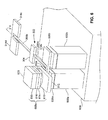
- FIGs 8 and 9 are views of a MEMS scanner housing 802 for use in a LBP.
- Two front plates 804a, 804b are fastened to a rear housing 806 with mounting screws 808a, 808b, 808c, 808d.
- MEMS scanner 302 is held in a cavity therein that allows for an appropriate amount of rotation.
- Threaded adjustment screw holes 810a, 810b, 810c, and 810d receive adjustment screws (not shown) that protrude into corresponding adjustment screw receiving bores 620 formed in third pressure plates 618 (shown in Figure 6 ). During assembly, adjustment screws are turned to provide an appropriate amount of preload on series disk spring 612 (not shown).
- MEMS observation port 812 formed in the top of rear housing 806.
- the MEMS scanner assembly 802 is secured to the exposure unit of a LBP via mounting tabs 814a, 814b formed in housing 806.
- clamps 608 to secure the MEMS scanner 302 in housing 802 results in a mount that "floats", allowing the mounting pads 314 to move a bit with respect to one another.
- slight twisting of the clamps 608 during assembly can result in slight in-plane twisting of the mounting pads 314. This can result in undesirable residual stress in the T-bars and/or torsion bars of the MEMS scanner.
- Such twisting may be reduced or eliminated by running or "burning-in" the mounted scanner for a few hours at reduced scan angle. In an exemplary embodiment, the scanner is run at half amplitude for approximately four hours. The burn-in process can reduce the occurrence of "infant" failures associated with mechanical failure of the T-bars and/or torsion arms.
- reduced twist clamp assembly designs may be substituted to reduce or eliminate the need for scanner assembly bum-in.
- the MEMS scanner 302 may be driven by four piezo-electric stacks 602, one juxtaposed against each mounting pad 314a, 314b, 314c, and 314d.
- one end of the MEMS scanner may be held in a fixed position, i.e. mounting pads 314c and 314d may be clamped against a solid mounting point, and the other end of the MEMS scanner may be driven by piezo-electric actuators, i.e. mounting pads 314a and 314b may each be clamped against piezo-electric stacks as shown in Figure 6 .
- three of the mounting pads are each clamped to a fixed, solid mounting point and one piezo-electric stack actuator is used.
- the choice hinges on cost vs. actuator power requirements are used.
- the MEMS scanner is trimmed to have a resonant frequency within a few hertz of the desired operational frequency.
- small changes in resonant frequency can result in relatively substantial changes in rotation amplitude (for a given periodic actuation voltage).
- the inventors have discovered that controlled heating of the MEMS device further trims the resonance frequency, and hence the actuation amplitude, even though in the exemplary embodiment the MEMS scanner has no outer frame.
- the extended tab on the first pressure plate 610 of clamp 608a receives a heater wire as does the corresponding pressure plate of clamp 608b (not shown).
- corresponding pressure plates adjacent mounting pads 314c and 314d also receive heater wires.
- the heater wires may be attached by soldering to the gold plated extended tab of first pressure plates 610, by soldering to metallized bond pad formed, for example on the mounting pads 314, or by other method as will be apparent to those skilled in the art.
- the scan amplitude is monitored by sensors and the electric potential between the two ends of scanner 302 (mounting pads 606a and 606b forming one such end and mounting pads 606c and 606d forming the other end) is adjusted. Resistance of the silicon material to current flow, and particularly the torsion arms 306a, 306b, causes joule heating.
Claims (37)
- Un scanner MEMS (302) pour une imprimante laser, comprenant :une plaque de balayage en silicium (304) possédant un axe de rotation (310), une première dimension parallèle à l'axe de rotation, une deuxième dimension perpendiculaire à l'axe de rotation,un premier et un deuxième bras de torsion opposés (306a, 306b), chaque bras de torsion étant couplé à la plaque de balayage (304) et s'étendant longitudinalement d'un point proximal à un point distal, les premier et deuxième bras de torsion (306a, 306b) définissant l'axe de rotation de la plaque de balayage (304), etune première (312a, 314a, 314b) et une deuxième (312b, 314c, 314d) structures de montage opposées, chaque structure de montage étant couplée à un point distal d'un bras de torsion respectif (306a, 306b),caractérisé en ce que ladite deuxième dimension est supérieure à 4 fois la première dimension, etcaractérisé en outre par :une première (308a, 316a, 316b, 318a) et une deuxième (308b, 316c, 316d, 318b) suspensions interposées entre la plaque de balayage (304) et des premier et deuxième bras de torsion respectifs (306a, 306b), les première (308a, 316a, 316b, 318a) et deuxième (308b, 316c, 316d, 318b) suspensions formant un appareil d'étalement de couple conçu de façon à maintenir une planéité dynamique du miroir (304) au cours du fonctionnement du scanner MEMS (302), etles première (308a, 316a, 316b, 318a) et deuxième (308b, 316c, 316d, 318b) suspensions comprennent des première et deuxième tiges de suspension respectives (308a, 308b) et les première et deuxième tiges de suspension (308a, 308b) sont couplées à la plaque de balayage en silicium (304) par des connecteurs centraux respectifs (318a, 318b) et des premier et deuxième connecteurs latéraux (316a, 316b, 316c, 316d) disposés le long de la deuxième dimension à partir du point axial.
- Le scanner MEMS (302) pour une imprimante laser selon la Revendication 1, où la plaque de balayage en silicium (304) possède une deuxième dimension supérieure à 8 fois sa première dimension.
- Le scanner MEMS (302) pour une imprimante laser selon la Revendication 2, où la plaque de balayage en silicium (304) possède une deuxième dimension de 8 millimètres et une première dimension de 750 micromètres.
- Le scanner MEMS (302) pour une imprimante laser selon la Revendication 1, où la plaque de balayage en silicium (304) et les premier et deuxième bras de torsion opposés (306a, 306b) ont une épaisseur de 700 micromètres.
- Le scanner MEMS (302) pour une imprimante laser selon la Revendication 1, où les premier et deuxième bras de torsion opposés (306a, 306b) possèdent chacun une longueur supérieure à 8 millimètres.
- Le scanner MEMS (302) pour une imprimante laser selon la Revendication 5, où les premier et deuxième bras de torsion opposés (306a, 306b) possèdent chacun une longueur de 8,76 millimètres.
- Le scanner MEMS (302) pour une imprimante laser selon la Revendication 1, où les premier et deuxième bras de torsion opposés (306a, 306b) possèdent chacun une largeur de 384 micromètres.
- Le scanner MEMS (302) pour une imprimante laser selon la Revendication 1, où les premier et deuxième bras de torsion opposés (306a, 306b) possèdent chacun une épaisseur supérieure à leur largeur.
- Le scanner MEMS (302) pour une imprimante laser selon la Revendication 1, où la première dimension de la plaque de balayage (304) est supérieure à la moitié de son épaisseur et inférieure à deux fois son épaisseur.
- Le scanner MEMS (302) pour une imprimante laser selon la Revendication 1, où les première (312a, 314a, 314b) et deuxième (312b, 3140, 314d) structures de montage opposées comprennent en outre :une première et une deuxième barres en T opposées (312a, 312b), chaque barre en T étant couplée à un point distal d'un bras de torsion respectif (306a, 306b) et s'étendant le long de la deuxième dimension dans des directions opposées à partir d'un point axial vers deux points latéraux équidistants de celui-ci, etdes premier, deuxième, troisième et quatrième plots de montage (314a, 314b, 314c, 314d), chaque plot de montage étant couplé à un point équidistant respectif d'une barre en T disposée le long de la deuxième dimension à partir du point axial.
- Le scanner MEMS (302) pour une imprimante laser selon la Revendication 10, où le premier bras de torsion (306a) est couplé à la première barre en T (312a) avec un premier et un deuxième filets elliptiques au niveau du point de couplage.
- Le scanner MEMS (302) pour une imprimante laser selon la Revendication 11, où les premier et deuxième filets elliptiques possèdent une dimension de 400 micromètres le long du bras de torsion (306a) et de 200 micromètres le long de la barre en T (312a).
- Le scanner MEMS (302) pour une imprimante laser selon la Revendication 10, où les points latéraux équidistants des barres en T (312a, 312b) sont décalés vers la plaque de balayage en silicium (304) dans la première direction en comparaison du point distal des bras de torsion (306a, 306b).
- Le scanner MEMS (302) pour une imprimante laser selon la Revendication 10, comprenant en outre au moins un actionneur piézo-électrique empilé (602a) soutenant au moins un plot de montage (314a).
- Le scanner MEMS (302) pour une imprimante laser selon la Revendication 14, où le au moins un actionneur piézo-électrique empilé (602a) comprend deux actionneurs piézo-électriques empilés (602a, 602b), chacun d'eux soutenant un plot de montage respectif (314a, 314b).
- Le scanner MEMS (302) pour une imprimante laser selon la Revendication 14, où le au moins un actionneur piézo-électrique empilé (602a) comprend quatre actionneurs piézo-électriques empilés (602a, 602b, 602c, 602c), chacun d'eux soutenant un plot de montage respectif (314a, 314b, 314c, 314d).
- Le scanner MEMS (302) pour une imprimante laser selon la Revendication 10, comprenant en outre :un logement (802) auquel les premier, deuxième, troisième et quatrième plots de montage (314a, 314b, 314c, 314d) sont fixés.
- Le scanner MEMS (302) selon la Revendication 17, où :les troisième et quatrième plots de montage (314c, 314d) sont fixés directement au logement (802),les premier et deuxième plots de montage (314a, 314b) sont fixés à un premier et un deuxième actionneurs piézo-électriques empilés respectifs (602a, 602a), etles premier et deuxième actionneurs piézo-électriques empilés (602a, 602b) sont maintenus en contact avec le logement (802).
- Le scanner MEMS (302) selon la Revendication 17, où les premier, deuxième, troisième et quatrième plots de montage (314a, 314b, 314c, 314d) sont fixés à des premier, deuxième, troisième et quatrième actionneurs piézo-électriques empilés respectifs (602a, 602b), et
les premier, deuxième, troisième et quatrième actionneurs piézo-électriques (602a, 602b) sont maintenus en contact avec le logement (802). - Le scanner MEMS (302) selon la Revendication 19, où les premier, deuxième, troisième et quatrième plots de montage (314a, 314b, 314c, 314d) sont fixés aux premier, deuxième, troisième et quatrième actionneurs piézo-électriques empilés respectifs (602a, 602b) de façon à exercer une force de compression préchargée sur les actionneurs piézo-électriques empilés respectifs (602a, 602b).
- Le scanner MEMS (302) pour une imprimante laser selon la Revendication 17, comprenant en outre une unité d'exposition d'imprimante laser (106) sur laquelle le logement est monté.
- Le scanner MEMS (302) pour une imprimante laser selon la Revendication 1, où la plaque de balayage (304) est conçue de façon à pivoter en va-et-vient périodiquement autour de l'axe de rotation (310) défini par les premier et deuxième bras de torsion (306a, 306b) à une fréquence supérieure à 1 kHz.
- Le scanner MEMS (302) pour une imprimante laser selon la Revendication 22, où la plaque de balayage (304) est conçue de façon à pivoter en va-et-vient périodiquement autour de l'axe de rotation (310) défini par les premier et deuxième bras de torsion (306a, 306b) à une fréquence de 5 kHz.
- Le scanner MEMS (302) pour une imprimante laser selon la Revendication 1, où la plaque de balayage (304) est conçue de façon à pivoter en va-et-vient périodiquement autour de l'axe de rotation (310) défini par les premier et deuxième bras de torsion (306a, 306b) vers un mouvement de rotation supérieur à un angle de balayage mécanique de zéro à crête de 10 degrés.
- Le scanner MEMS (302) pour une imprimante laser selon la Revendication 24, où la plaque de balayage (304) est conçue de façon à pivoter en va-et-vient périodiquement autour de l'axe de rotation (310) défini par les premier et deuxième bras de torsion (306a, 306b) vers un mouvement de rotation d'un angle de balayage mécanique de zéro à crête de 20 degrés.
- Le scanner MEMS (302) pour une imprimante laser selon la Revendication 1, où les première et deuxième tiges de suspension (308a, 308b) possèdent chacune une première dimension inférieure à la première dimension de la plaque de balayage en silicium (304).
- Le scanner MEMS (302) pour une imprimante laser selon la Revendication 1, où le scanner MEMS (302) est formé photolithographiquement à partir d'une plaquette de silicium (502).
- Le scanner MEMS (302) pour une imprimante laser selon la Revendication 1, où la plaque de balayage en silicium (304), les premier et deuxième bras de torsion opposés (306a, 306b) et les première (312a, 314a, 314b) et deuxième (312b, 314c, 314d) structures de montage opposées sont formés avec une épaisseur constante correspondant à l'épaisseur d'une plaquette de silicium (502).
- Le scanner MEMS (302) pour une imprimante laser selon la Revendication 1, comprenant en outre :un miroir formé sur une surface de la plaque de balayage en silicium (304).
- Le scanner MEMS (302) pour une imprimante laser selon la Revendication 29, où le miroir possède une réflectivité supérieure à 90% à une longueur d'onde de 650 nanomètres.
- Le scanner MEMS (302) pour une imprimante laser selon la Revendication 30, où le miroir possède une réflectivité supérieure à 95% à une longueur d'onde de 650 nanomètres.
- Le scanner MEMS (302) pour une imprimante laser selon la Revendication 1, comprenant en outre un premier et un deuxième fils de dispositif de chauffage couplés fonctionnellement aux première (312a, 314a, 314b) et deuxième (312b, 314c, 314d) structures de montage opposées respectives.
- Le scanner MEMS (302) pour une imprimante laser selon la Revendication 32, où les premier et deuxième fils de dispositif de chauffage sont conçus de façon à créer un potentiel électrique sur les premier et deuxième bras de torsion (306a, 306b).
- Le scanner MEMS (302) pour une imprimante laser selon la Revendication 33, où les premier et deuxième fils de dispositif de chauffage sont conçus de façon à induire un chauffage par effet Joule à l'intérieur des premier et deuxième bras de torsion (306a, 306b).
- Un procédé d'actionnement d'une imprimante laser, comprenant :la modulation d'un laser (202) avec des données d'image de façon à produire un faisceau laser modulé,la mise en forme du faisceau laser modulé de façon à produire un faisceau laser modulé mis en forme,la déflexion périodique du faisceau laser modulé mis en forme de façon à produire un faisceau laser modulé mis en forme balayé, etl'alignement du faisceau laser modulé mis en forme balayé de façon à empiéter sur un photoconducteur pivotant (102) destiné à produire une image électrostatique latente correspondant aux données vidéo sur le photoconducteur,où la déflexion périodique du faisceau laser modulé mis en forme est exécutée par le scanner MEMS (302) selon l'une quelconque des Revendications 1 à 34.
- Une imprimante électrophotographique, comprenant :un photoconducteur (102) conçu de façon à, en succession, recevoir une charge statique, recevoir une lumière modulée destinée à former une image électrostatique latente, recevoir du toner dans un motif correspondant à l'image électrostatique latente et transférer le toner vers un rouleau de réception, etune unité d'exposition (106) conçue de façon à fournir une lumière modulée au photoconducteur (102), l'unité d'exposition comprenant :une source de lumière (202) réactive à un signal modulé,des optiques de mise en forme de faisceau (204) alignées de façon à recevoir de la lumière provenant de la source de lumière et à produire un faisceau de lumière mis en forme, etle scanner MEMS (302) selon l'une quelconque des Revendications 1 à 34.
- L'utilisation d'un scanner MEMS (302) selon l'une quelconque des Revendications 1 à 34 dans une imprimante électrophotographique, l'imprimante électrophotographique comprenant :un photoconducteur (102) conçu de façon à, en succession, recevoir une charge statique, recevoir une lumière modulée de façon à former une image électrostatique latente, recevoir du toner dans un motif correspondant à l'image électrostatique latente et transférer le toner vers un rouleau de réception, etune unité d'exposition (106) conçue de façon à fournir une lumière modulée au photoconducteur (102), l'unité d'exposition comprenant :une source de lumière (202) réactive à un signal modulé,des optiques de mise en forme de faisceau (204) alignées de façon à recevoir de la lumière provenant de la source de lumière et à produire un faisceau de lumière mis en forme, etle scanner MEMS (302) aligné de façon à recevoir le faisceau de lumière mis en forme et conçu de façon à balayer périodiquement la lumière sur le photoconducteur (102).
Applications Claiming Priority (2)
| Application Number | Priority Date | Filing Date | Title |
|---|---|---|---|
| US54289604P | 2004-02-09 | 2004-02-09 | |
| PCT/US2005/004066 WO2005078507A1 (fr) | 2004-02-09 | 2005-02-09 | Scanneur de systemes microelectromecaniques conçu pour imprimante laser |
Publications (2)
| Publication Number | Publication Date |
|---|---|
| EP1723460A1 EP1723460A1 (fr) | 2006-11-22 |
| EP1723460B1 true EP1723460B1 (fr) | 2014-07-16 |
Family
ID=34860350
Family Applications (1)
| Application Number | Title | Priority Date | Filing Date |
|---|---|---|---|
| EP05713179.9A Not-in-force EP1723460B1 (fr) | 2004-02-09 | 2005-02-09 | Scanneur de systemes microelectromecaniques concu pour imprimante laser |
Country Status (5)
| Country | Link |
|---|---|
| EP (1) | EP1723460B1 (fr) |
| JP (1) | JP4528787B2 (fr) |
| KR (1) | KR101091129B1 (fr) |
| CN (1) | CN100492096C (fr) |
| WO (1) | WO2005078507A1 (fr) |
Cited By (1)
| Publication number | Priority date | Publication date | Assignee | Title |
|---|---|---|---|---|
| US10018723B2 (en) | 2012-07-26 | 2018-07-10 | Apple Inc. | Dual-axis scanning mirror |
Families Citing this family (11)
| Publication number | Priority date | Publication date | Assignee | Title |
|---|---|---|---|---|
| US7187483B1 (en) * | 2005-09-16 | 2007-03-06 | Texas Instruments Incorporated | Magnet on frame oscillating device |
| US7898561B2 (en) * | 2007-01-26 | 2011-03-01 | Miradia Inc. | MEMS mirror system for laser printing applications |
| JP2009223246A (ja) * | 2008-03-19 | 2009-10-01 | Hitachi Ltd | ミラー駆動方法ならびにそれを用いた表示装置 |
| JP5095569B2 (ja) | 2008-09-17 | 2012-12-12 | 株式会社リコー | 光走査装置及び画像形成装置 |
| WO2011133815A2 (fr) * | 2010-04-21 | 2011-10-27 | Mezmeriz, Inc. | Systèmes de miroir à balayage composite |
| JP5659672B2 (ja) * | 2010-10-06 | 2015-01-28 | セイコーエプソン株式会社 | 光スキャナー、ミラーチップ、光スキャナーの製造方法、および画像形成装置 |
| JP6260019B2 (ja) * | 2012-11-09 | 2018-01-17 | 北陽電機株式会社 | 金属弾性部材、微小機械装置、微小機械装置の製造方法、揺動制御装置及び揺動制御方法 |
| WO2014126542A1 (fr) | 2013-02-13 | 2014-08-21 | Tenu Elektroni̇k Sanayi̇ Ve Ti̇caret Li̇mi̇ted Şi̇rketi̇ | Système d'éclairage utilisé dans des véhicules |
| US9670056B2 (en) * | 2014-01-31 | 2017-06-06 | Stmicroelectronics S.R.L. | Electrostatically driven MEMS device |
| CN104924776A (zh) * | 2014-03-17 | 2015-09-23 | 联想(北京)有限公司 | 一种打印设备的激光扫描单元 |
| US11372344B2 (en) | 2016-10-10 | 2022-06-28 | Hp Indigo B.V. | Controlling scan-to-scan spacing between print operations |
Citations (3)
| Publication number | Priority date | Publication date | Assignee | Title |
|---|---|---|---|---|
| US20030053156A1 (en) * | 2001-08-20 | 2003-03-20 | Yukito Satoh | Optical scanning device and image forming apparatus using the same |
| US6672732B1 (en) * | 1999-08-28 | 2004-01-06 | Robert Bosch Gmbh | Micromechanical oscillating device |
| EP1553752A1 (fr) * | 2003-12-26 | 2005-07-13 | Seiko Epson Corporation | Appareil à balayage optique et dispositif de formation d'images |
Family Cites Families (5)
| Publication number | Priority date | Publication date | Assignee | Title |
|---|---|---|---|---|
| US5999306A (en) | 1995-12-01 | 1999-12-07 | Seiko Epson Corporation | Method of manufacturing spatial light modulator and electronic device employing it |
| US6850475B1 (en) | 1996-07-30 | 2005-02-01 | Seagate Technology, Llc | Single frequency laser source for optical data storage system |
| JP2001264676A (ja) * | 2000-03-14 | 2001-09-26 | Olympus Optical Co Ltd | 光スキャナ |
| US7068296B2 (en) | 2001-09-14 | 2006-06-27 | Ricoh Company, Ltd. | Optical scanning device for reducing a dot position displacement at a joint of scanning lines |
| US6760144B2 (en) | 2001-12-05 | 2004-07-06 | Jds Uniphase Corporation | Articulated MEMS electrostatic rotary actuator |
-
2005
- 2005-02-09 CN CNB2005800108068A patent/CN100492096C/zh not_active Expired - Fee Related
- 2005-02-09 KR KR1020067018626A patent/KR101091129B1/ko active IP Right Grant
- 2005-02-09 JP JP2006553202A patent/JP4528787B2/ja not_active Expired - Fee Related
- 2005-02-09 WO PCT/US2005/004066 patent/WO2005078507A1/fr active Application Filing
- 2005-02-09 EP EP05713179.9A patent/EP1723460B1/fr not_active Not-in-force
Patent Citations (3)
| Publication number | Priority date | Publication date | Assignee | Title |
|---|---|---|---|---|
| US6672732B1 (en) * | 1999-08-28 | 2004-01-06 | Robert Bosch Gmbh | Micromechanical oscillating device |
| US20030053156A1 (en) * | 2001-08-20 | 2003-03-20 | Yukito Satoh | Optical scanning device and image forming apparatus using the same |
| EP1553752A1 (fr) * | 2003-12-26 | 2005-07-13 | Seiko Epson Corporation | Appareil à balayage optique et dispositif de formation d'images |
Cited By (1)
| Publication number | Priority date | Publication date | Assignee | Title |
|---|---|---|---|---|
| US10018723B2 (en) | 2012-07-26 | 2018-07-10 | Apple Inc. | Dual-axis scanning mirror |
Also Published As
| Publication number | Publication date |
|---|---|
| CN100492096C (zh) | 2009-05-27 |
| CN101002131A (zh) | 2007-07-18 |
| KR101091129B1 (ko) | 2011-12-09 |
| JP4528787B2 (ja) | 2010-08-18 |
| JP2007526506A (ja) | 2007-09-13 |
| KR20070117436A (ko) | 2007-12-12 |
| EP1723460A1 (fr) | 2006-11-22 |
| WO2005078507A1 (fr) | 2005-08-25 |
Similar Documents
| Publication | Publication Date | Title |
|---|---|---|
| EP1723460B1 (fr) | Scanneur de systemes microelectromecaniques concu pour imprimante laser | |
| US7636101B2 (en) | MEMS scanner adapted to a laser printer | |
| US7031040B2 (en) | Optical scanning apparatus, optical writing apparatus, image forming apparatus, and method of driving vibration mirror | |
| JP2007322466A (ja) | 光偏向器、及びそれを用いた光学機器 | |
| JP5728823B2 (ja) | 光偏向器、光走査装置、画像形成装置及び画像投影装置 | |
| US7656570B2 (en) | Optical deflector and optical instrument using the same | |
| US7649301B2 (en) | Actuator capable of driving with large rotational angle or large deflection angle | |
| JP5500016B2 (ja) | 光偏向器、光走査装置、画像形成装置及び画像投影装置 | |
| US7474165B2 (en) | Oscillating device, optical deflector and optical instrument using the same | |
| JP5614167B2 (ja) | 光偏向器、光走査装置、画像形成装置及び画像投影装置 | |
| JP4390174B2 (ja) | 光走査装置 | |
| US20100150612A1 (en) | Oscillator device and method of manufacturing the same | |
| JP4172627B2 (ja) | 振動ミラー、光書込装置及び画像形成装置 | |
| WO2009011405A1 (fr) | Dispositif oscillateur et déflecteur optique l'utilisant | |
| US8681408B2 (en) | Optical scanning device, image forming apparatus, and image projection device | |
| JP2006195290A (ja) | 画像読取装置及び画像形成装置 | |
| EP2851733B1 (fr) | Dispositif de déviation optique et appareil de formation d'images | |
| JP2008070863A (ja) | 振動ミラー、光書込装置および画像形成装置 | |
| US20100302612A1 (en) | Oscillating structure and oscillator device using the same | |
| JP2007171929A (ja) | 揺動体装置、光偏向器、及びそれを用いた光学機器 | |
| JP2009031642A (ja) | 揺動体装置、光偏向器およびそれを用いた画像形成装置 | |
| JP2009031643A (ja) | 揺動体装置、光偏向器およびそれを用いた画像形成装置 | |
| JP2004341320A (ja) | 光走査装置、画像形成装置 | |
| JP2003029191A (ja) | 光偏向器及びそれを用いた光学機器 | |
| JP2009109905A (ja) | 振動ミラー、光走査装置、光書込装置、画像形成装置 |
Legal Events
| Date | Code | Title | Description |
|---|---|---|---|
| PUAI | Public reference made under article 153(3) epc to a published international application that has entered the european phase |
Free format text: ORIGINAL CODE: 0009012 |
|
| 17P | Request for examination filed |
Effective date: 20060908 |
|
| AK | Designated contracting states |
Kind code of ref document: A1 Designated state(s): AT BE BG CH CY CZ DE DK EE ES FI FR GB GR HU IE IS IT LI LT LU MC NL PL PT RO SE SI SK TR |
|
| DAX | Request for extension of the european patent (deleted) | ||
| 17Q | First examination report despatched |
Effective date: 20070529 |
|
| GRAP | Despatch of communication of intention to grant a patent |
Free format text: ORIGINAL CODE: EPIDOSNIGR1 |
|
| INTG | Intention to grant announced |
Effective date: 20140129 |
|
| RAP1 | Party data changed (applicant data changed or rights of an application transferred) |
Owner name: MICROVISION, INC. Owner name: SEIKO EPSON CORPORATION |
|
| GRAS | Grant fee paid |
Free format text: ORIGINAL CODE: EPIDOSNIGR3 |
|
| GRAA | (expected) grant |
Free format text: ORIGINAL CODE: 0009210 |
|
| AK | Designated contracting states |
Kind code of ref document: B1 Designated state(s): AT BE BG CH CY CZ DE DK EE ES FI FR GB GR HU IE IS IT LI LT LU MC NL PL PT RO SE SI SK TR |
|
| REG | Reference to a national code |
Ref country code: GB Ref legal event code: FG4D |
|
| REG | Reference to a national code |
Ref country code: DE Ref legal event code: R081 Ref document number: 602005044192 Country of ref document: DE Owner name: MICROVISION, INC., REDMOND, US Free format text: FORMER OWNERS: MICROVISION, INC., REDMOND, WASH., US; SEIKO EPSON CORP., SUWA, NAGANO, JP |
|
| REG | Reference to a national code |
Ref country code: CH Ref legal event code: EP |
|
| REG | Reference to a national code |
Ref country code: IE Ref legal event code: FG4D |
|
| REG | Reference to a national code |
Ref country code: AT Ref legal event code: REF Ref document number: 677971 Country of ref document: AT Kind code of ref document: T Effective date: 20140815 |
|
| REG | Reference to a national code |
Ref country code: DE Ref legal event code: R096 Ref document number: 602005044192 Country of ref document: DE Effective date: 20140828 |
|
| REG | Reference to a national code |
Ref country code: NL Ref legal event code: VDEP Effective date: 20140716 |
|
| REG | Reference to a national code |
Ref country code: AT Ref legal event code: MK05 Ref document number: 677971 Country of ref document: AT Kind code of ref document: T Effective date: 20140716 |
|
| REG | Reference to a national code |
Ref country code: LT Ref legal event code: MG4D |
|
| PG25 | Lapsed in a contracting state [announced via postgrant information from national office to epo] |
Ref country code: PT Free format text: LAPSE BECAUSE OF FAILURE TO SUBMIT A TRANSLATION OF THE DESCRIPTION OR TO PAY THE FEE WITHIN THE PRESCRIBED TIME-LIMIT Effective date: 20141117 Ref country code: SE Free format text: LAPSE BECAUSE OF FAILURE TO SUBMIT A TRANSLATION OF THE DESCRIPTION OR TO PAY THE FEE WITHIN THE PRESCRIBED TIME-LIMIT Effective date: 20140716 Ref country code: BG Free format text: LAPSE BECAUSE OF FAILURE TO SUBMIT A TRANSLATION OF THE DESCRIPTION OR TO PAY THE FEE WITHIN THE PRESCRIBED TIME-LIMIT Effective date: 20141016 Ref country code: GR Free format text: LAPSE BECAUSE OF FAILURE TO SUBMIT A TRANSLATION OF THE DESCRIPTION OR TO PAY THE FEE WITHIN THE PRESCRIBED TIME-LIMIT Effective date: 20141017 Ref country code: LT Free format text: LAPSE BECAUSE OF FAILURE TO SUBMIT A TRANSLATION OF THE DESCRIPTION OR TO PAY THE FEE WITHIN THE PRESCRIBED TIME-LIMIT Effective date: 20140716 Ref country code: ES Free format text: LAPSE BECAUSE OF FAILURE TO SUBMIT A TRANSLATION OF THE DESCRIPTION OR TO PAY THE FEE WITHIN THE PRESCRIBED TIME-LIMIT Effective date: 20140716 Ref country code: FI Free format text: LAPSE BECAUSE OF FAILURE TO SUBMIT A TRANSLATION OF THE DESCRIPTION OR TO PAY THE FEE WITHIN THE PRESCRIBED TIME-LIMIT Effective date: 20140716 |
|
| PG25 | Lapsed in a contracting state [announced via postgrant information from national office to epo] |
Ref country code: PL Free format text: LAPSE BECAUSE OF FAILURE TO SUBMIT A TRANSLATION OF THE DESCRIPTION OR TO PAY THE FEE WITHIN THE PRESCRIBED TIME-LIMIT Effective date: 20140716 Ref country code: AT Free format text: LAPSE BECAUSE OF FAILURE TO SUBMIT A TRANSLATION OF THE DESCRIPTION OR TO PAY THE FEE WITHIN THE PRESCRIBED TIME-LIMIT Effective date: 20140716 Ref country code: IS Free format text: LAPSE BECAUSE OF FAILURE TO SUBMIT A TRANSLATION OF THE DESCRIPTION OR TO PAY THE FEE WITHIN THE PRESCRIBED TIME-LIMIT Effective date: 20141116 Ref country code: NL Free format text: LAPSE BECAUSE OF FAILURE TO SUBMIT A TRANSLATION OF THE DESCRIPTION OR TO PAY THE FEE WITHIN THE PRESCRIBED TIME-LIMIT Effective date: 20140716 Ref country code: CY Free format text: LAPSE BECAUSE OF FAILURE TO SUBMIT A TRANSLATION OF THE DESCRIPTION OR TO PAY THE FEE WITHIN THE PRESCRIBED TIME-LIMIT Effective date: 20140716 |
|
| REG | Reference to a national code |
Ref country code: DE Ref legal event code: R097 Ref document number: 602005044192 Country of ref document: DE |
|
| PG25 | Lapsed in a contracting state [announced via postgrant information from national office to epo] |
Ref country code: SK Free format text: LAPSE BECAUSE OF FAILURE TO SUBMIT A TRANSLATION OF THE DESCRIPTION OR TO PAY THE FEE WITHIN THE PRESCRIBED TIME-LIMIT Effective date: 20140716 Ref country code: IT Free format text: LAPSE BECAUSE OF FAILURE TO SUBMIT A TRANSLATION OF THE DESCRIPTION OR TO PAY THE FEE WITHIN THE PRESCRIBED TIME-LIMIT Effective date: 20140716 Ref country code: DK Free format text: LAPSE BECAUSE OF FAILURE TO SUBMIT A TRANSLATION OF THE DESCRIPTION OR TO PAY THE FEE WITHIN THE PRESCRIBED TIME-LIMIT Effective date: 20140716 Ref country code: CZ Free format text: LAPSE BECAUSE OF FAILURE TO SUBMIT A TRANSLATION OF THE DESCRIPTION OR TO PAY THE FEE WITHIN THE PRESCRIBED TIME-LIMIT Effective date: 20140716 Ref country code: EE Free format text: LAPSE BECAUSE OF FAILURE TO SUBMIT A TRANSLATION OF THE DESCRIPTION OR TO PAY THE FEE WITHIN THE PRESCRIBED TIME-LIMIT Effective date: 20140716 Ref country code: RO Free format text: LAPSE BECAUSE OF FAILURE TO SUBMIT A TRANSLATION OF THE DESCRIPTION OR TO PAY THE FEE WITHIN THE PRESCRIBED TIME-LIMIT Effective date: 20140716 |
|
| PLBE | No opposition filed within time limit |
Free format text: ORIGINAL CODE: 0009261 |
|
| STAA | Information on the status of an ep patent application or granted ep patent |
Free format text: STATUS: NO OPPOSITION FILED WITHIN TIME LIMIT |
|
| 26N | No opposition filed |
Effective date: 20150417 |
|
| PG25 | Lapsed in a contracting state [announced via postgrant information from national office to epo] |
Ref country code: BE Free format text: LAPSE BECAUSE OF NON-PAYMENT OF DUE FEES Effective date: 20150228 |
|
| PG25 | Lapsed in a contracting state [announced via postgrant information from national office to epo] |
Ref country code: LU Free format text: LAPSE BECAUSE OF FAILURE TO SUBMIT A TRANSLATION OF THE DESCRIPTION OR TO PAY THE FEE WITHIN THE PRESCRIBED TIME-LIMIT Effective date: 20150209 |
|
| REG | Reference to a national code |
Ref country code: CH Ref legal event code: PL |
|
| PG25 | Lapsed in a contracting state [announced via postgrant information from national office to epo] |
Ref country code: CH Free format text: LAPSE BECAUSE OF NON-PAYMENT OF DUE FEES Effective date: 20150228 Ref country code: MC Free format text: LAPSE BECAUSE OF FAILURE TO SUBMIT A TRANSLATION OF THE DESCRIPTION OR TO PAY THE FEE WITHIN THE PRESCRIBED TIME-LIMIT Effective date: 20140716 Ref country code: LI Free format text: LAPSE BECAUSE OF NON-PAYMENT OF DUE FEES Effective date: 20150228 |
|
| REG | Reference to a national code |
Ref country code: DE Ref legal event code: R082 Ref document number: 602005044192 Country of ref document: DE Representative=s name: DENDORFER & HERRMANN PATENTANWAELTE PARTNERSCH, DE Ref country code: DE Ref legal event code: R081 Ref document number: 602005044192 Country of ref document: DE Owner name: MICROVISION, INC., REDMOND, US Free format text: FORMER OWNERS: MICROVISION, INC., REDMOND, WASH., US; SEIKO EPSON CORP., SUWA, NAGANO, JP |
|
| REG | Reference to a national code |
Ref country code: IE Ref legal event code: MM4A |
|
| PG25 | Lapsed in a contracting state [announced via postgrant information from national office to epo] |
Ref country code: SI Free format text: LAPSE BECAUSE OF FAILURE TO SUBMIT A TRANSLATION OF THE DESCRIPTION OR TO PAY THE FEE WITHIN THE PRESCRIBED TIME-LIMIT Effective date: 20140716 |
|
| REG | Reference to a national code |
Ref country code: GB Ref legal event code: 732E Free format text: REGISTERED BETWEEN 20151112 AND 20151118 |
|
| REG | Reference to a national code |
Ref country code: FR Ref legal event code: PLFP Year of fee payment: 12 |
|
| PG25 | Lapsed in a contracting state [announced via postgrant information from national office to epo] |
Ref country code: IE Free format text: LAPSE BECAUSE OF NON-PAYMENT OF DUE FEES Effective date: 20150209 |
|
| PG25 | Lapsed in a contracting state [announced via postgrant information from national office to epo] |
Ref country code: BE Free format text: LAPSE BECAUSE OF FAILURE TO SUBMIT A TRANSLATION OF THE DESCRIPTION OR TO PAY THE FEE WITHIN THE PRESCRIBED TIME-LIMIT Effective date: 20140716 |
|
| REG | Reference to a national code |
Ref country code: FR Ref legal event code: TP Owner name: MICROVISION, INC., US Effective date: 20161115 |
|
| REG | Reference to a national code |
Ref country code: FR Ref legal event code: PLFP Year of fee payment: 13 |
|
| PG25 | Lapsed in a contracting state [announced via postgrant information from national office to epo] |
Ref country code: HU Free format text: LAPSE BECAUSE OF FAILURE TO SUBMIT A TRANSLATION OF THE DESCRIPTION OR TO PAY THE FEE WITHIN THE PRESCRIBED TIME-LIMIT; INVALID AB INITIO Effective date: 20050209 |
|
| PG25 | Lapsed in a contracting state [announced via postgrant information from national office to epo] |
Ref country code: TR Free format text: LAPSE BECAUSE OF FAILURE TO SUBMIT A TRANSLATION OF THE DESCRIPTION OR TO PAY THE FEE WITHIN THE PRESCRIBED TIME-LIMIT Effective date: 20140716 |
|
| REG | Reference to a national code |
Ref country code: FR Ref legal event code: PLFP Year of fee payment: 14 |
|
| PGFP | Annual fee paid to national office [announced via postgrant information from national office to epo] |
Ref country code: FR Payment date: 20190111 Year of fee payment: 15 Ref country code: GB Payment date: 20190206 Year of fee payment: 15 Ref country code: DE Payment date: 20190129 Year of fee payment: 15 |
|
| REG | Reference to a national code |
Ref country code: DE Ref legal event code: R119 Ref document number: 602005044192 Country of ref document: DE |
|
| GBPC | Gb: european patent ceased through non-payment of renewal fee |
Effective date: 20200209 |
|
| PG25 | Lapsed in a contracting state [announced via postgrant information from national office to epo] |
Ref country code: FR Free format text: LAPSE BECAUSE OF NON-PAYMENT OF DUE FEES Effective date: 20200229 Ref country code: DE Free format text: LAPSE BECAUSE OF NON-PAYMENT OF DUE FEES Effective date: 20200901 Ref country code: GB Free format text: LAPSE BECAUSE OF NON-PAYMENT OF DUE FEES Effective date: 20200209 |