EP1714321B1 - Montage et procédé pour protéger un circuit intégré à semi-conducteur - Google Patents
Montage et procédé pour protéger un circuit intégré à semi-conducteur Download PDFInfo
- Publication number
- EP1714321B1 EP1714321B1 EP05707380A EP05707380A EP1714321B1 EP 1714321 B1 EP1714321 B1 EP 1714321B1 EP 05707380 A EP05707380 A EP 05707380A EP 05707380 A EP05707380 A EP 05707380A EP 1714321 B1 EP1714321 B1 EP 1714321B1
- Authority
- EP
- European Patent Office
- Prior art keywords
- circuit
- control
- detector
- switching
- protection circuit
- Prior art date
- Legal status (The legal status is an assumption and is not a legal conclusion. Google has not performed a legal analysis and makes no representation as to the accuracy of the status listed.)
- Expired - Fee Related
Links
Images


Classifications
-
- H—ELECTRICITY
- H01—ELECTRIC ELEMENTS
- H01L—SEMICONDUCTOR DEVICES NOT COVERED BY CLASS H10
- H01L27/00—Devices consisting of a plurality of semiconductor or other solid-state components formed in or on a common substrate
- H01L27/02—Devices consisting of a plurality of semiconductor or other solid-state components formed in or on a common substrate including semiconductor components specially adapted for rectifying, oscillating, amplifying or switching and having at least one potential-jump barrier or surface barrier; including integrated passive circuit elements with at least one potential-jump barrier or surface barrier
- H01L27/0203—Particular design considerations for integrated circuits
- H01L27/0248—Particular design considerations for integrated circuits for electrical or thermal protection, e.g. electrostatic discharge [ESD] protection
- H01L27/0251—Particular design considerations for integrated circuits for electrical or thermal protection, e.g. electrostatic discharge [ESD] protection for MOS devices
- H01L27/0259—Particular design considerations for integrated circuits for electrical or thermal protection, e.g. electrostatic discharge [ESD] protection for MOS devices using bipolar transistors as protective elements
- H01L27/0262—Particular design considerations for integrated circuits for electrical or thermal protection, e.g. electrostatic discharge [ESD] protection for MOS devices using bipolar transistors as protective elements including a PNP transistor and a NPN transistor, wherein each of said transistors has its base coupled to the collector of the other transistor, e.g. silicon controlled rectifier [SCR] devices
-
- H—ELECTRICITY
- H01—ELECTRIC ELEMENTS
- H01L—SEMICONDUCTOR DEVICES NOT COVERED BY CLASS H10
- H01L27/00—Devices consisting of a plurality of semiconductor or other solid-state components formed in or on a common substrate
- H01L27/02—Devices consisting of a plurality of semiconductor or other solid-state components formed in or on a common substrate including semiconductor components specially adapted for rectifying, oscillating, amplifying or switching and having at least one potential-jump barrier or surface barrier; including integrated passive circuit elements with at least one potential-jump barrier or surface barrier
- H01L27/04—Devices consisting of a plurality of semiconductor or other solid-state components formed in or on a common substrate including semiconductor components specially adapted for rectifying, oscillating, amplifying or switching and having at least one potential-jump barrier or surface barrier; including integrated passive circuit elements with at least one potential-jump barrier or surface barrier the substrate being a semiconductor body
-
- H—ELECTRICITY
- H01—ELECTRIC ELEMENTS
- H01L—SEMICONDUCTOR DEVICES NOT COVERED BY CLASS H10
- H01L27/00—Devices consisting of a plurality of semiconductor or other solid-state components formed in or on a common substrate
- H01L27/02—Devices consisting of a plurality of semiconductor or other solid-state components formed in or on a common substrate including semiconductor components specially adapted for rectifying, oscillating, amplifying or switching and having at least one potential-jump barrier or surface barrier; including integrated passive circuit elements with at least one potential-jump barrier or surface barrier
Definitions
- the invention relates to a circuit arrangement for protecting a semiconductor integrated circuit with a protective circuit, which includes a thyristor structure and is connected between a protected element and a reference potential, and with a control circuit for driving the protection circuit and a corresponding method for protecting a semiconductor integrated circuit.
- Integrated semiconductor (IC) circuits can be damaged by transient pulses or overvoltages that are coupled via leads (pads) or directly into lines, so that they become inoperable or even destroyed.
- Such pulses or overvoltages can occur, for example, in so-called electrostatic discharges (English: ESD, Electrostatic Discharge).
- ESD Electrostatic Discharge
- such a pulse e.g., burst
- a pulse may occur in many fields of application, e.g. In automotive engineering, for example, there is a need to design such circuits, which must operate in the high-voltage range up to 90 volts or above, also for significantly higher interference pulse levels.
- An alternative for such breakthrough-based protection concepts is an active circuit for protecting an integrated circuit, consisting of a combination of an active trigger circuit with a known protection device such as a thyristor or a bipolar or MOS protection transistor.
- Active circuits to protect the IC are often triggered by the rise of the transient signal.
- the signal rise per unit of time is detected and a protective transistor or a protective circuit is switched through via a drive circuit.
- the protective circuit can therefore be understood as an actively triggered overvoltage or overcurrent arrester. In the event of a fault, rapid control of the protection circuit is necessary.
- a SCR Silicon Controlled Rectifier
- the thyristor is realized in the semiconductor device in a conventional manner by means of an n-well, a p-well and highly doped n and p regions.
- the transient voltage is detected with an RC element.
- the voltage level detected at the capacitance is converted into a control signal which drives the base of the pnp transistor of the thyristor structure.
- the npn transistor of the thyristor structure turns on, so that the transient pulse is derived by the low-resistance thyristor from the pad potential of the I / O pin to reference potential.
- the thyristor then remains automatically turned on until its current falls below the holding current and the extinguishing condition is met.
- the invention has for its object to provide a circuit arrangement and a method for protecting semiconductor integrated circuits, which allow improved performance. Furthermore, a circuit arrangement and a method are to be specified, which are particularly suitable for high-voltage processes or for high-voltage applications.
- the invention has the advantage that the circuit arrangement as an actively triggered protection circuit and the corresponding Procedure to enable a quick turn on the thyristor structure. Further, the invention can be integrated in high voltage applications fabricated using high voltage processes.
- a terminal PV is connected to a line LV, which is at a potential VV.
- the potential VV may be, for example, the positive supply potential VDD or the potential of an input / output terminal (I / O pad).
- the PV connection or LV cable must be protected against transient pulses or against overvoltage. This overvoltage must be derived against a reference potential VB, which may be, for example, the ground potential.
- the reference potential VB leading line LB is connected to the terminal PB.
- the actual task of deriving interference pulses or overvoltages fulfills the protective circuit PC, which is designated in all exemplary embodiments as SCR.
- the protection circuit PC or SCR is controlled or triggered by a control circuit TC, which is connected on the input side to the terminals PV and PB.
- the control circuit TC includes a detector circuit capable of detecting the transient pulses appearing at the terminal PV and the line and generating control signals for the protection circuit PC and SCR, respectively.
- the control circuit TC generates a plurality of control signals, which respectively control an active element of the protection circuit PC or SCR.
- control signals which respectively control an active element of the protection circuit PC or SCR.
- These are the signals CTL and CTH, which drive the transistors T1 and T2, respectively.
- the active elements of the protection circuit PC or SCR are connected in such a way that they are actuated by the control signals the trigger or control circuit TC establish a low-resistance connection between the line LV and the terminal PV and the reference potential VB.
- the protection circuit PC or SCR can also derive higher currents against reference potential VB.
- the protection circuit PC or SCR contains a thyristor structure.
- a thyristor is a four-layer component, which is shown in the equivalent circuit diagram as two interconnected bipolar transistors.
- the control circuit TC controls in case of failure, the two transistors T1 and T2 (T10 and T20 in Fig. 4 respectively.
- Fig. 5 of the thyristor structure of the protection circuit with two control signals active. For this purpose, currents are injected directly into the two base-emitter junctions.
- the protection circuit is designed as a thyristor SCR with the two transistors T1 and T2.
- T1 is a pnp transistor connected to its emitter at the voltage carrying line LV, while T2 an npn transistor is connected on the emitter side to the reference potential VB.
- the collectors of the two transistors are cross-connected to the base of the other transistor.
- such a transistor structure can be realized in a manner known per se by means of an n- or p-well with well resistors RN or RP and correspondingly arranged highly doped regions, see FIG. 6 or schematically the FIGS. 3 to 5 , In the FIGS. 1 and 2 are the resistors Rn and RP not shown for a better understanding of the operation.
- the control circuit is in the FIG. 1b ) realized by a detector circuit with downstream inverters.
- the detector circuit is designed as an RC element consisting of the series connection of a capacitor C1 and a resistor R1, which is connected to the lines LV and LB and the corresponding terminals PV and PB.
- Inverters are connected downstream of the connection node of the capacitor C1 and the resistor R1 , the output side respectively the bases of the transistors T1 and T2 drive.
- the inverter I1 is connected to the base of the transistor T1 and two series-connected inverters I2 and I3 to the base of the transistor T2.
- the inverters are necessary in order to convert the potential applied at the connection point of the capacitor C1 and the resistor R1 into defined control signals CTL and CTH which drive the transistor elements of the thyristor SCR.
- the detector circuit of capacitance C1 and resistor R1 forms as RC element a complex voltage divider, at whose center tap the voltage increase of the interference pulse is detected.
- the capacitance C1 becomes low, so that at the starting point of the detector circuit sets a high potential.
- the output signal CTL switches to low potential, so that the pn junction between emitter and base of T1 exceeds the switching threshold and T1 turns on.
- the inverters I2 and I3, which are connected in series, are connected in parallel with I1 and convert the voltage signal detected at the tap node of the detector circuit into a defined control signal CTH for driving the NPN transistor T2.
- T2 switches to the conducting state almost at the same time as T1.
- the thyristor SCR becomes conductive and the transient pulse present on the line LV or the connection PV can be derived against the reference potential.
- the example according to Figure 1c ) differs from the example FIG. 1b ) in that the detector circuit of the capacitive and the resistive device in the opposite direction to the terminals PV and PB is connected.
- the resistor R11 is at the terminal PV and the capacitor C11 is at the terminal PB.
- the voltage conditions at the output of the detector circuit namely the connection point of R11 and C11 rotate, so that the control of the transistor T1 and T2 must be done differently.
- the series circuit of the inverters I4 and I5 is connected downstream of the output of the detector circuit in order to drive the transistor T1. In parallel with these inverters, the output of the detector circuit is followed by the inverter I6, which activates the transistor T2.
- the capacitance C11 becomes low, so that at the starting point of the detector circuit set a low potential.
- the inverter I6 converts this low potential into a voltage required for the control of the transistor T2 or a corresponding control current.
- the series-connected inverters I4 and 15 convert the output voltage at the capacitor C11 into a control signal of low potential or a corresponding current, so that the transistor T1 turns on.
- the detector circuit is in the examples of FIG. 1 designed as an RC element, but not limited thereto.
- Other embodiments of the detector circuit may be useful, as long as the essential function, namely the detection of a transient pulse to be derived on the voltage-carrying line LV and the generation of control signals for the control of the active elements or semiconductor junctions of the protection circuit, in the embodiment of the transistors of the thyristor SCR, are functionally fulfilled.
- the decisive factor is that the transient signal is detected on the one hand and on the other hand, the thyristor SCR is not ignited in normal operation.
- the time constant of the RC element determines on the one hand the detection of a transient pulse and on the other hand the time during which the detector circuit is active. A pulse is detected and detected as long as the rise time of the transient disturbance is less than the time constant of the RC element.
- the time constant determined by the decay of the pulse, the time after which the detector circuit is inactive and shuts down or returns to normal operation.
- a small capacitance of the RC element for example realized as a gate oxide capacity
- the resistance of this capacitance is low in transient processes, so that in the example of the FIG. 1b ) the output of the RC element is brought very fast to high potential, while the output of the detector circuit in the Figure 1c ) is brought to low potential very quickly.
- the resistances of the capacitors of the RC element in both examples act as high-impedance components, so that in the FIG. 1b ) the output of the detector circuit is kept at low potential while in the circuit Figure 1c ) is kept at high potential.
- FIG. 2 show a second example.
- an additional circuit is provided which determines how long the control circuit remains active. It can thus be ensured that the control signals of the control circuit control the thyristor SCR at least until the transient pulse on the line LV or the terminal PV has decayed with certainty.
- the inverters I1, I2 and I3 correspond to the example of FIG. 1b ) in this order in the FIG. 2a ) the inverters I20, 130 and I40.
- the function of this inverter in the FIG. 2a ) is identical to the inverters of the first example, but the dimensioning and implementation of the inverters can be implemented in different ways.
- an inverter I10 is connected as an element of the additional circuit, which drives a PMOS transistor P10.
- this transistor is connected on the one hand to the voltage-carrying line LV and on the other hand to the inputs of the inverters I20 and I30.
- the parallel connection of a second RC element of the capacitor C21 and the resistor R21 is also connected, which are connected with their other terminal respectively to the reference potential VB and the line LB.
- this is detected by the first RC element.
- the output of this first RC element which drives the inverter I10, assumes a high pulse at a fast pulse rise through the then low-resistance capacitance C12, so that the inverter I10 is brought to the low side on the output side.
- the rise time of the transient disturbance on the line LV must be shorter than the time constant of the first RC element.
- the PMOS transistor P10 With the then low-impedance output of the inverter I10, the PMOS transistor P10 is turned on, the output of which sets the inverter inputs of the inverters 120 and I30 to a high potential. As with the example of the FIG. 1b ), subsequently the transistors T1 and T2 are turned on, so that the thyrister SCR becomes conductive and can dissipate the pulse on the line LV to reference potential.
- the time constant of the second RC element of the elements C21 and R21 can be set independently of the time constant of the first RC element and determines in this situation how long the control circuit remains active and generates control signals to the transistors T1 and T2.
- inverters I20, I30 and I40 are capable of generating the control currents for the turn-on of transistors T1 and T2.
- P10 switches off eg because the transient pulse flattens out and the time constant of the first RC element becomes shorter than the voltage changes on the line LV
- the connection node of the inputs of the inverters I20 and I30 with the second RC element becomes via this RC element and discharge its time constant against reference potential.
- the time constant of the second RC element is adjusted so that the control circuit outputs the control signals to the thyristor as long as the transient fault persists. This means that the time constant of the second RC element is greater than the time constant of the first RC element. In this way, different transient pulse shapes can be detected and derived by means of the first and the second RC element. Furthermore, the time constants of the two RC elements can be optimized independently of each other with regard to their function.
- FIG. 2b differs from the example of FIG. 2a in that the inverters are embodied concretely as CMOS inverters I11, I21, I31 and I41.
- the active triggered protection circuit concepts described above make use of inverters.
- the inverters provide the voltages or currents with the necessary short signal rise times to trigger the actual protection circuit.
- inverters in high-voltage applications, in turn, is not completely unproblematic.
- High-voltage components which are manufactured using high-voltage processes, often have asymmetrical operating parameters or operating conditions, which are due to the nature of the high-voltage process, in particular the multiple insulation wells.
- the maximum allowable drain-source voltage of a MOS transistor may be considerably higher than the corresponding maximum allowable gate bulk voltage. Therefore, certain device configurations, such as e.g. Standard inverters, not manufactured for the possible voltage ranges.
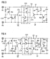
- the control circuit is in FIG. 3 realized by a detector circuit with downstream control transistors TH1 and TL1 as output switching elements.
- the detector circuit includes two subcircuits, one of which drives transistor T1 and the other drives transistor T2.
- each detector subcircuit for transient detection an RC element of the series connection of a capacitance and a resistor which is connected to the lines LV and LB and the corresponding terminals PV and PB.
- Each detector subcircuit of capacitance and resistance forms as RC element a complex voltage divider, at whose center tap the voltage increase of the interference pulse is detected.
- the (complex) resistance of the capacitance low ("low"), so that sets a low or high potential at the output node of the detector circuit depending on the polarity of the RC circuit.
- the node voltage reaches the switching threshold of the detector transistor (TD1 or TD2), it switches on and generates at its output a potential that can drive and switch through the control transistors (TH1 or TL1).
- the output voltages of the switched control transistors cause the pn junction between the emitter and base of T1 and T2 exceeds the switching threshold and turns on the protection circuit.
- the detector subcircuit for driving T1 is made up of the series connection of a capacitor C13 and a resistor R13.
- the connection node of the capacitor C13 and the resistor R13, the transistor TD1 is connected downstream.
- TD1 is formed as a p-channel transistor.
- TD1 controls the output side of the n-channel control transistor TL1.
- TL1 is connected on the output side to the base of T1.
- the resistance of C13 becomes low, so that TD1 turns on and the output of TD1 assumes high potential, in particular VV, and drives TL1.
- the output of TL1 or the base of T1 are thereby set to reference potential VB and T1 turns on.
- the detector subcircuit for driving T2 differs from the detector subcircuit for driving T1 in that the RC series circuit of the capacitive and the resistive device is connected in the opposite direction to the terminals PV and PB.
- the resistor R2 is connected to the terminal PB and the capacitor C2 to the terminal PV.
- connection node of the capacitor C2 and the resistor R2, the transistor TD2 is connected downstream.
- TD is formed as an n-channel transistor.
- TD2 controls the output side of the p-channel control transistor TH1.
- TH1 has its output connected to the base of T2.
- the resistance of C2 becomes low, so that TD2 switches and the output of TD2 becomes low, in particular VB, and can drive TH1 through.
- the output of TH1 and the base of T2 are thereby set to high potential VV and T2 turns on.
- detector circuit may be useful as long as the essential function described above is met.
- the decisive factor is that the transient signal is detected on the one hand, and on the other hand, in normal operation, the thyristor SCR not ignited.
- the time constant of the RC element determines the detection of a transient pulse.
- T2 switches to the conducting state at the same time or almost simultaneously with T1.
- the thyristor SCR becomes conductive and the transient pulse present on the line LV or the connection PV can be derived against the reference potential.
- R3, C3 and R4, C4 determine how long the control circuit remains active or after which time the protection circuit SCR is turned off again. It can thus be ensured that the control signals of the control circuit control the thyristor SCR at least until the transient pulse on the line LV or the terminal PV has decayed with certainty.
- the parallel connection of a further RC element of the capacitor C3 and the resistor R3 is connected between the base terminal of the transistor TL1 and reference potential VB. Between the base terminal of the transistor TH1 and high potential VV, the parallel connection of an RC element of the capacitor C4 and the resistor R4 is connected.
- the time constants of the RC element from the elements C3, R3 and C4, R4 can be set independently of the associated time constant of the RC element of C13, R13 or C2, R2 and determine how long the control circuit remains active and the control signals abut the transistors T1 and T2. As long as TL1 or TH1 remain switched through, you can TL1 and TH1 generate the control currents for the connection of the transistors T1 and T2.
- the time constants R3, C3 and R4, C4 are set so that the control circuit will output the control signals to the protection circuit as long as the transient fault persists.
- the time constants of C3 and R3 or C4 and R4 when the transistors TD1 and TD2 are switched off, the inputs of the control transistors TL1 and TH1 are blocked and the control currents of T1 and T2 are switched off.
- time constants By setting the time constants, different transient pulse shapes can be detected and derived. Furthermore, the time constants of the RC elements can be independently optimized with regard to their function.
- FIG. 4 shows a further embodiment of the invention, which is compared to the embodiment of the FIG. 3 essentially differs in that additional gate driver transistors are used. This makes it possible to improve the switching behavior of the control or trigger transistors TH10 and TL10.
- transistor T11 as a gate driver for TD10 requires reversing the polarity of the detecting RC element so that C10 is connected to VV and R10 is connected to VB.
- the n-channel driver transistor T12 in the output circuit of TD10 drives the p-channel switching transistor TH10, which in turn drives T20.
- the p-channel driver transistor T13 in the output circuit of TD20 drives the n-channel switching transistor TL10, which in turn drives T10.
- control circuit for detecting the transient event and for driving T1 or T2 is constructed from two subcircuits or subcircuits, which are assigned separately to each of the transistors T1 and T2.
- the separate implementation of the subcircuits of the control circuit allows independent dimensioning and optimization of these subcircuits.
- the further embodiment according to FIG. 5 differs from the embodiment of FIG. 4 in that both control transistors TL10 and TH10 with upstream driver transistors T13 and T12 use the same detector circuit.
- T12 serves not only to drive TH10, but also to drive the gate driver transistor T13 and the downstream switching element TL10.
- the elements C10, R10, T11, TD10 and C30, R30 are provided only once in the protection circuit.
- the elements R20, C20, R40, C40, TD20 and T21 of the second detector subcircuit may be omitted.
- the use of single transistors in the control circuit requires no inverters to trigger the protection circuit SCR.
- An optimization of the individual transistors, which are used as switching elements of the control circuit is possible in every manufacturing process of the integrated circuit, in particular in high-voltage processes, but also in standard processes. Thus, even using a high-voltage process as well as low-voltage processes, an optimized protection circuit can be produced.
- the invention is not limited to the use of MOS transistors as switching elements.
- bipolar transistors can be used as switching elements.
- the structure of the protective device in the semiconductor device is the embodiment according to FIG. 6 at.
- a low p-doped well 10 is arranged.
- the well 10 may also be the substrate of the semiconductor.
- an n-doped well 20 is arranged in the tub 10.
- the thyristor of T1 and T2 is embedded in the embodiment using a high-voltage process in the n-well 20.
- the n-well 20 serves to control the high voltages occurring.
- highly doped regions with p- or n-conductivity are arranged, which can be generated in a conventional manner, for example by implantation or diffusion.
- the highly doped n-region 21 and the highly doped p-region 22 can be separately connected to a potential, but they must have the same potential during operation. For this purpose, they are each connected to the high potential VV.
- the heavily doped n-region 23 is connected to the output CTL of the control circuit.
- a p-doped well 30 is arranged in the n-well 20.
- two highly doped p-regions 31 and 33 and a highly doped n-region 32 are arranged. These may be fabricated by implantation or diffusion in a conventional manner similar to the heavily doped regions of the n-well.
- the regions 32 and 33 can be separately connected to a potential, but they must have the same potential during operation. In the example, they are each connected to the reference potential VB.
- the region 31 is connected to the output CTH of the control circuit.
- field plates P11 and P12 are made of polysilicon (typically as a polylayer).
- the field plates serve to control the electric field at the high operating voltages and increase the breakdown voltage of the device. This results in a lower susceptibility of the circuit against false triggering.
- the parasitic thyristor structure with the transistors T1 and T2 is shown in the n- or p-well. Thereafter, the collector of the npn transistor T2 results between the region 21 with a downstream resistor RN of the n-well 20 and the region 23. The base results from the region 31 and the collector of T1 and is connected via the resistor RP of the p-type. Tub 30 connected to reference potential VB. The base of this transistor T2 is connected to the region 31 as a control terminal to which the control signal CTH for turning on and off of the transistor can be applied. The emitter results as area 32.
- the base of the pnp transistor T1 results between the region 21 and the downstream path resistance RN of the n-well 20 and the collector of the transistor T2 and the region 23, to which the signal CTL is applied.
- the collector of T1 results between terminal 33 with downstream track resistance RP of the p-well 30 and the area 31.
- the emitter of the transistor T1 is connected to the area 22.
- the control signal CTL is used to turn on or off the transistor T1.
- the control lines or control signals CTL and CTH are first set to low potential (range 23) or high potential (range 31) to the transistors T1 and T2 turn.
- a base current for the pnp or npn transistor is provided. The base currents turn on the respective transistor and thus ignite the thyristor.
- the protective function between the lines LV and LB is in operation.
- the region 23 is set to high potential via the connection CTL after switching off the control transistor TL1 means of the rail resistor RN and the area 31 via the terminal CTH after switching off the control transistor TH1 by means of the web resistance RP to low potential. This locks the transistors T1 and T2 and thus the thyristor.
Abstract
Claims (8)
- Montage de circuits destiné à protéger un circuit intégré à semiconducteur, comportant- un circuit de protection (PC ; SCR) qui contient une structure de thyristor (T1, T2 ; T10, T20) comprenant deux éléments actifs et qui est monté entre un élément à protéger (VV) et un potentiel de référence (VB), et comportant- un circuit de commande (TC ; R2, C2, TD2, TH1, R13, C13, TD1, TL1) qui est configuré pour commander le circuit de protection et qui est monté en parallèle au circuit de protection entre l'élément à protéger et le potentiel de référence (VB),- le circuit de commande contenant un circuit de détection (R2, C2, TD2, R13, C13, TD1) et deux éléments de commutation (TH1, TL1) configurés comme transistors individuels, lesquels sont chacun reliés au circuit de détection sur leur entrée de commande et génèrent des signaux de commande (CTH, CTL) sur leur sortie et commandent chacun un élément actif (T1, T2) du circuit de protection (SCR),- les bornes de sortie de l'un des éléments de commutation (TH1) étant reliées à l'un des deux éléments actifs (T2) du circuit de protection d'un côté et à l'élément à protéger de l'autre,- les bornes de sortie de l'autre élément de commutation (TL1) étant reliées à l'autre des deux éléments actifs (T1) du circuit de protection d'un côté et au potentiel de référence (VB) de l'autre,- un premier et un deuxième circuit parallèle d'un circuit RC servant à commander une opération de déconnexion, dont le premier circuit parallèle est disposé entre l'entrée de commande d'un élément de commutation (TH1) et l'élément à protéger et le deuxième circuit parallèle entre l'entrée de commande de l'autre élément de commutation (TL1) et le potentiel de référence (VB).
- Montage de circuits selon la revendication 1, où les transistors individuels des éléments de commutation sont de type de conductibilité différent et commandent le circuit de protection de façon antipolaire.
- Montage de circuits selon la revendication 1 ou 2, où un élément pilote (T12, T13) est monté en aval de chacun des deux éléments de commutation (TH10, TL10).
- Montage de circuits selon l'une des revendications 1 à 3, où le circuit de détection contient au moins un élément de commutation de détection (TD10 ; TD20).
- Montage de circuits selon l'une des revendications 1 à 4, où les éléments de commutation sont configurés comme transistors MOS ou bipolaires (TH1, TL1 ; TH10, TL10).
- Montage de circuits selon l'une des revendications 1 à 5, où le circuit de détection contient un premier circuit RC (R2, C2 ; R13, C13) constitué d'une résistance et d'une capacité et est conçu pour détecter une montée de signal avec un temps de montée prédéfini au niveau de l'élément à protéger (PV, LV).
- Montage de circuits selon l'une des revendications 1 à 6, où le circuit de détection est constitué de deux circuits de détection partiels qui commandent chacun l'un des deux éléments de commutation (TH1, TL1).
- Montage de circuits selon l'une des revendications 1 à 7, où les entrées de commande des éléments actifs du circuit de protection sont réalisées dans une structure de semiconducteur moyennant des cuves de type de conductibilité différent, dans lesquelles sont disposées des zones fortement dopées pour les circuits de sortie des éléments actifs (T1, T2).
Applications Claiming Priority (3)
| Application Number | Priority Date | Filing Date | Title |
|---|---|---|---|
| DE200410007241 DE102004007241A1 (de) | 2004-02-13 | 2004-02-13 | Schaltungsanordnung und Verfahren zum Schutz einer integrierten Halbleiterschaltung |
| DE200410056222 DE102004056222A1 (de) | 2004-11-22 | 2004-11-22 | Schaltungsanordnung und Verfahren zum Schutz einer integrierten Halbleiterschaltung |
| PCT/EP2005/001476 WO2005078798A2 (fr) | 2004-02-13 | 2005-02-14 | Montage et procede pour proteger un circuit integre a semi-conducteur |
Publications (2)
| Publication Number | Publication Date |
|---|---|
| EP1714321A2 EP1714321A2 (fr) | 2006-10-25 |
| EP1714321B1 true EP1714321B1 (fr) | 2010-05-12 |
Family
ID=34862906
Family Applications (1)
| Application Number | Title | Priority Date | Filing Date |
|---|---|---|---|
| EP05707380A Expired - Fee Related EP1714321B1 (fr) | 2004-02-13 | 2005-02-14 | Montage et procédé pour protéger un circuit intégré à semi-conducteur |
Country Status (6)
| Country | Link |
|---|---|
| US (1) | US7738222B2 (fr) |
| EP (1) | EP1714321B1 (fr) |
| JP (1) | JP4651044B2 (fr) |
| KR (1) | KR100914790B1 (fr) |
| DE (1) | DE502005009563D1 (fr) |
| WO (1) | WO2005078798A2 (fr) |
Families Citing this family (28)
| Publication number | Priority date | Publication date | Assignee | Title |
|---|---|---|---|---|
| DE502005009563D1 (de) | 2004-02-13 | 2010-06-24 | Austriamicrosystems Ag | Schaltungsanordnung und Verfahren zum Schutz einer integrierten Halbleiterschaltung |
| US7956418B2 (en) * | 2007-05-29 | 2011-06-07 | Mediatek Inc. | ESD protection devices |
| DE102007040875B4 (de) | 2007-08-29 | 2017-11-16 | Austriamicrosystems Ag | Schaltungsanordnung zum Schutz vor elektrostatischen Entladungen und Verfahren zum Betreiben einer solchen |
| KR100942956B1 (ko) * | 2008-02-12 | 2010-02-17 | 주식회사 하이닉스반도체 | 에스씨알 회로를 이용한 정전기 방전 장치 |
| WO2010032603A1 (fr) * | 2008-09-19 | 2010-03-25 | Semiconductor Energy Laboratory Co., Ltd. | Dispositif à semi-conducteurs et étiquette sans fil l'utilisant |
| US8693148B2 (en) * | 2009-01-08 | 2014-04-08 | Micron Technology, Inc. | Over-limit electrical condition protection circuits for integrated circuits |
| EP2246886A1 (fr) * | 2009-04-27 | 2010-11-03 | STmicroelectronics SA | Circuit intégré muni d'une protection de grande surface contre les décharges électrostatiques |
| US8284530B1 (en) * | 2009-08-31 | 2012-10-09 | Texas Instruments Incorporated | Electrostatic discharge (ESD) protection circuit and related apparatus and method |
| US8619395B2 (en) | 2010-03-12 | 2013-12-31 | Arc Suppression Technologies, Llc | Two terminal arc suppressor |
| US8320091B2 (en) * | 2010-03-25 | 2012-11-27 | Analog Devices, Inc. | Apparatus and method for electronic circuit protection |
| US8861158B2 (en) * | 2010-04-21 | 2014-10-14 | Cypress Semiconductor Corporation | ESD trigger for system level ESD events |
| US8422187B2 (en) | 2010-07-02 | 2013-04-16 | Analog Devices, Inc. | Apparatus and method for electronic circuit protection |
| KR20120084659A (ko) | 2011-01-20 | 2012-07-30 | 가부시키가이샤 한도오따이 에네루기 켄큐쇼 | 급전 장치 및 비접촉 급전 시스템 |
| TWI469306B (zh) * | 2011-04-29 | 2015-01-11 | Faraday Tech Corp | 靜電放電保護電路 |
| DE102011109596B4 (de) | 2011-08-05 | 2018-05-09 | Austriamicrosystems Ag | Schaltungsanordnung zum Schutz gegen elektrostatische Entladungen |
| US8724268B2 (en) | 2011-08-30 | 2014-05-13 | Micron Technology, Inc. | Over-limit electrical condition protection circuits and methods |
| US8947844B2 (en) * | 2012-05-14 | 2015-02-03 | Middle Alantic Products, Inc. | Series type surge suppressor and clamping circuit |
| US8958187B2 (en) | 2012-11-09 | 2015-02-17 | Analog Devices, Inc. | Active detection and protection of sensitive circuits against transient electrical stress events |
| US9293912B2 (en) | 2013-09-11 | 2016-03-22 | Analog Devices, Inc. | High voltage tolerant supply clamp |
| US9634482B2 (en) | 2014-07-18 | 2017-04-25 | Analog Devices, Inc. | Apparatus and methods for transient overstress protection with active feedback |
| US10199369B2 (en) | 2016-03-04 | 2019-02-05 | Analog Devices, Inc. | Apparatus and methods for actively-controlled transient overstress protection with false condition shutdown |
| US10177566B2 (en) * | 2016-06-21 | 2019-01-08 | Analog Devices, Inc. | Apparatus and methods for actively-controlled trigger and latch release thyristor |
| US10734806B2 (en) * | 2016-07-21 | 2020-08-04 | Analog Devices, Inc. | High voltage clamps with transient activation and activation release control |
| US10861845B2 (en) | 2016-12-06 | 2020-12-08 | Analog Devices, Inc. | Active interface resistance modulation switch |
| US10608431B2 (en) | 2017-10-26 | 2020-03-31 | Analog Devices, Inc. | Silicon controlled rectifier dynamic triggering and shutdown via control signal amplification |
| US11387648B2 (en) | 2019-01-10 | 2022-07-12 | Analog Devices International Unlimited Company | Electrical overstress protection with low leakage current for high voltage tolerant high speed interfaces |
| CN111697549B (zh) * | 2019-03-14 | 2021-11-12 | 中芯国际集成电路制造(上海)有限公司 | Esd保护电路以及电子器件 |
| US11817697B2 (en) | 2022-04-05 | 2023-11-14 | International Business Machines Corporation | Method to limit the time a semiconductor device operates above a maximum operating voltage |
Family Cites Families (21)
| Publication number | Priority date | Publication date | Assignee | Title |
|---|---|---|---|---|
| EP0822596A3 (fr) | 1996-08-02 | 2000-01-05 | Texas Instruments Inc. | Circuit de protection ESD |
| US5781388A (en) * | 1996-09-03 | 1998-07-14 | Motorola, Inc. | Non-breakdown triggered electrostatic discharge protection circuit for an integrated circuit and method therefor |
| JP4144901B2 (ja) | 1996-11-07 | 2008-09-03 | 株式会社ルネサステクノロジ | 半導体集積回路装置 |
| US6091593A (en) * | 1997-10-22 | 2000-07-18 | Winbond Electronics Corp. | Early trigger of ESD protection device by a negative voltage pump circuit |
| KR20000008809A (ko) | 1998-07-16 | 2000-02-15 | 피영준 | 한방녹심원의 제조방법 |
| US5982601A (en) * | 1998-07-30 | 1999-11-09 | Winbond Electronics Corp. | Direct transient-triggered SCR for ESD protection |
| US6233130B1 (en) * | 1998-07-30 | 2001-05-15 | Winbond Electronics Corp. | ESD Protection device integrated with SCR |
| KR20000008809U (ko) * | 1998-10-28 | 2000-05-25 | 김영환 | 저전력 풀-업 및 풀-다운 구동 회로 |
| US6618233B1 (en) | 1999-08-06 | 2003-09-09 | Sarnoff Corporation | Double triggering mechanism for achieving faster turn-on |
| US6552886B1 (en) * | 2000-06-29 | 2003-04-22 | Pericom Semiconductor Corp. | Active Vcc-to-Vss ESD clamp with hystersis for low supply chips |
| TW473977B (en) * | 2000-10-27 | 2002-01-21 | Vanguard Int Semiconduct Corp | Low-voltage triggering electrostatic discharge protection device and the associated circuit |
| US6803633B2 (en) * | 2001-03-16 | 2004-10-12 | Sarnoff Corporation | Electrostatic discharge protection structures having high holding current for latch-up immunity |
| CN1190841C (zh) | 2001-08-20 | 2005-02-23 | 旺宏电子股份有限公司 | 静电放电保护装置 |
| US6747861B2 (en) * | 2001-11-15 | 2004-06-08 | Industrial Technology Research Institute | Electrostatic discharge protection for a mixed-voltage device using a stacked-transistor-triggered silicon controlled rectifier |
| JP3901671B2 (ja) * | 2003-08-19 | 2007-04-04 | 松下電器産業株式会社 | 半導体集積回路装置 |
| DE502005009563D1 (de) | 2004-02-13 | 2010-06-24 | Austriamicrosystems Ag | Schaltungsanordnung und Verfahren zum Schutz einer integrierten Halbleiterschaltung |
| DE102004007241A1 (de) | 2004-02-13 | 2005-09-01 | Austriamicrosystems Ag | Schaltungsanordnung und Verfahren zum Schutz einer integrierten Halbleiterschaltung |
| DE102004029008A1 (de) | 2004-06-16 | 2006-01-05 | Austriamicrosystems Ag | Schutzanordnung für eine Halbleiterschaltungsanordnung mit einer Thyristorstruktur und Verfahren zu ihrem Betrieb |
| US7212387B2 (en) * | 2004-09-17 | 2007-05-01 | Texas Instruments Incorporated | Electrostatic discharge protection device including precharge reduction |
| JP4504850B2 (ja) * | 2005-03-17 | 2010-07-14 | パナソニック株式会社 | 半導体集積回路装置 |
| US7545614B2 (en) * | 2005-09-30 | 2009-06-09 | Renesas Technology America, Inc. | Electrostatic discharge device with variable on time |
-
2005
- 2005-02-14 DE DE502005009563T patent/DE502005009563D1/de active Active
- 2005-02-14 JP JP2006552569A patent/JP4651044B2/ja active Active
- 2005-02-14 WO PCT/EP2005/001476 patent/WO2005078798A2/fr active Application Filing
- 2005-02-14 KR KR1020067016180A patent/KR100914790B1/ko active IP Right Grant
- 2005-02-14 EP EP05707380A patent/EP1714321B1/fr not_active Expired - Fee Related
- 2005-02-14 US US10/588,984 patent/US7738222B2/en active Active
Also Published As
| Publication number | Publication date |
|---|---|
| US7738222B2 (en) | 2010-06-15 |
| WO2005078798A3 (fr) | 2005-10-13 |
| US20080285199A1 (en) | 2008-11-20 |
| JP2007523476A (ja) | 2007-08-16 |
| KR20060127133A (ko) | 2006-12-11 |
| EP1714321A2 (fr) | 2006-10-25 |
| JP4651044B2 (ja) | 2011-03-16 |
| WO2005078798A2 (fr) | 2005-08-25 |
| DE502005009563D1 (de) | 2010-06-24 |
| KR100914790B1 (ko) | 2009-09-02 |
Similar Documents
| Publication | Publication Date | Title |
|---|---|---|
| EP1714321B1 (fr) | Montage et procédé pour protéger un circuit intégré à semi-conducteur | |
| DE19518549C2 (de) | MOS-Transistor getriggerte Schutzschaltung gegen elektrostatische Überspannungen von CMOS-Schaltungen | |
| DE19518550C2 (de) | Eingangsschutzschaltung für eine MOS-Einrichtung | |
| DE19533958C2 (de) | Schutzschaltung gegen elektrostatische Entladungen enthaltend eine Kondensatorschaltung | |
| DE102017112963B4 (de) | Schaltungen, Einrichtungen und Verfahren zum Schutz vor transienten Spannungen | |
| DE102010045325B4 (de) | ESD-Schutzschaltung | |
| DE102011018450B4 (de) | Halbleiterbauelement mit durchgeschalteten parasitären Thyristor bei einem Lichtangriff und Halbleiterbauelement mit Alarmschaltung für einen Lichtangriff | |
| EP0538507B1 (fr) | Circuit de protection pour contacts de connexion de circuits intégrés monolithiques | |
| DE102016106309A1 (de) | Hochgeschwindigkeits-Schnittstellenschutzvorrichtung | |
| EP0275872B1 (fr) | Circuit intégré avec circuit de protection contre l'effet "latch-up" dans la technique des circuits MOS-complémentaires | |
| DE102004009981A1 (de) | ESD-Schutzschaltkreis mit Kollektorstrom-gesteuerter Zündung für eine monolithisch integrierte Schaltung | |
| DE102011056317A1 (de) | Halbleiter-ESD-Schaltung und Verfahren | |
| EP1679746A2 (fr) | Dispositif, circuit et système de protection contre les décharges électrostatiques (ESD) | |
| DE102008036834A1 (de) | Diodenbasiertes ESE-Konzept für Demos-Schutz | |
| DE102021101690A1 (de) | Verfahren zum schützen eines schaltkreises, elektrostatische-entladung-schaltkreis und integrierter schaltkreis | |
| EP0261370A2 (fr) | Circuit integré ayant un circuit anti virrouillage fabriqué en technologie MOS complémentaire | |
| EP0261371B1 (fr) | Circuit intégré ayant un circuit anti virrouillage fabriqué en technologie MOS complémentaire | |
| DE112004002717T5 (de) | Pufferschaltung mit elektrostatischem Entladeschutz | |
| DE19738181C2 (de) | Schutzschaltkreis für integrierte Schaltungen | |
| DE102013203076B4 (de) | Vorrichtung mit Erkennung des Latch-Up-Effekts und Verfahren zum Bilden dieser Vorrichtung | |
| DE102004007241A1 (de) | Schaltungsanordnung und Verfahren zum Schutz einer integrierten Halbleiterschaltung | |
| DE102006026691B4 (de) | ESD-Schutzschaltung und -verfahren | |
| DE102009039247B4 (de) | Halbleiterkörper mit einer Anschlusszelle | |
| WO2005124863A1 (fr) | Systeme de protection pour circuit a semi-conducteurs comprenant une structure de thyristor et procede pour faire fonctionner ce systeme | |
| EP0379199B1 (fr) | Structure de protection ESD |
Legal Events
| Date | Code | Title | Description |
|---|---|---|---|
| PUAI | Public reference made under article 153(3) epc to a published international application that has entered the european phase |
Free format text: ORIGINAL CODE: 0009012 |
|
| 17P | Request for examination filed |
Effective date: 20060609 |
|
| AK | Designated contracting states |
Kind code of ref document: A2 Designated state(s): DE FR GB IE IT |
|
| RIN1 | Information on inventor provided before grant (corrected) |
Inventor name: CHOJECKI, PAWEL Inventor name: MAYERHOFER, MICHAEL Inventor name: FANKHAUSER, BERND Inventor name: DEUTSCHMANN, BERND |
|
| 17Q | First examination report despatched |
Effective date: 20061201 |
|
| DAX | Request for extension of the european patent (deleted) | ||
| RBV | Designated contracting states (corrected) |
Designated state(s): DE FR GB IE IT |
|
| RTI1 | Title (correction) |
Free format text: CIRCUIT ARRANGEMENT AND METHOD FOR PROTECTING AN INTEGRATED SEMICONDUCTOR CIRCUIT |
|
| GRAP | Despatch of communication of intention to grant a patent |
Free format text: ORIGINAL CODE: EPIDOSNIGR1 |
|
| GRAS | Grant fee paid |
Free format text: ORIGINAL CODE: EPIDOSNIGR3 |
|
| GRAA | (expected) grant |
Free format text: ORIGINAL CODE: 0009210 |
|
| AK | Designated contracting states |
Kind code of ref document: B1 Designated state(s): DE FR GB IE IT |
|
| REG | Reference to a national code |
Ref country code: GB Ref legal event code: FG4D Free format text: NOT ENGLISH |
|
| REG | Reference to a national code |
Ref country code: IE Ref legal event code: FG4D Free format text: LANGUAGE OF EP DOCUMENT: GERMAN |
|
| REF | Corresponds to: |
Ref document number: 502005009563 Country of ref document: DE Date of ref document: 20100624 Kind code of ref document: P |
|
| PLBE | No opposition filed within time limit |
Free format text: ORIGINAL CODE: 0009261 |
|
| STAA | Information on the status of an ep patent application or granted ep patent |
Free format text: STATUS: NO OPPOSITION FILED WITHIN TIME LIMIT |
|
| 26N | No opposition filed |
Effective date: 20110215 |
|
| PGFP | Annual fee paid to national office [announced via postgrant information from national office to epo] |
Ref country code: IE Payment date: 20110223 Year of fee payment: 7 |
|
| PGFP | Annual fee paid to national office [announced via postgrant information from national office to epo] |
Ref country code: DE Payment date: 20110218 Year of fee payment: 7 Ref country code: FR Payment date: 20110309 Year of fee payment: 7 Ref country code: IT Payment date: 20110223 Year of fee payment: 7 |
|
| REG | Reference to a national code |
Ref country code: DE Ref legal event code: R097 Ref document number: 502005009563 Country of ref document: DE Effective date: 20110214 |
|
| PGFP | Annual fee paid to national office [announced via postgrant information from national office to epo] |
Ref country code: GB Payment date: 20110223 Year of fee payment: 7 |
|
| GBPC | Gb: european patent ceased through non-payment of renewal fee |
Effective date: 20120214 |
|
| REG | Reference to a national code |
Ref country code: IE Ref legal event code: MM4A |
|
| REG | Reference to a national code |
Ref country code: FR Ref legal event code: ST Effective date: 20121031 |
|
| PG25 | Lapsed in a contracting state [announced via postgrant information from national office to epo] |
Ref country code: IT Free format text: LAPSE BECAUSE OF NON-PAYMENT OF DUE FEES Effective date: 20120214 |
|
| REG | Reference to a national code |
Ref country code: DE Ref legal event code: R119 Ref document number: 502005009563 Country of ref document: DE Effective date: 20120901 |
|
| PG25 | Lapsed in a contracting state [announced via postgrant information from national office to epo] |
Ref country code: IE Free format text: LAPSE BECAUSE OF NON-PAYMENT OF DUE FEES Effective date: 20120214 Ref country code: FR Free format text: LAPSE BECAUSE OF NON-PAYMENT OF DUE FEES Effective date: 20120229 Ref country code: GB Free format text: LAPSE BECAUSE OF NON-PAYMENT OF DUE FEES Effective date: 20120214 |
|
| PG25 | Lapsed in a contracting state [announced via postgrant information from national office to epo] |
Ref country code: DE Free format text: LAPSE BECAUSE OF NON-PAYMENT OF DUE FEES Effective date: 20120901 |