EP1714321B1 - Circuit arrangement and method for protecting an integrated semiconductor circuit - Google Patents
Circuit arrangement and method for protecting an integrated semiconductor circuit Download PDFInfo
- Publication number
- EP1714321B1 EP1714321B1 EP05707380A EP05707380A EP1714321B1 EP 1714321 B1 EP1714321 B1 EP 1714321B1 EP 05707380 A EP05707380 A EP 05707380A EP 05707380 A EP05707380 A EP 05707380A EP 1714321 B1 EP1714321 B1 EP 1714321B1
- Authority
- EP
- European Patent Office
- Prior art keywords
- circuit
- control
- detector
- switching
- protection circuit
- Prior art date
- Legal status (The legal status is an assumption and is not a legal conclusion. Google has not performed a legal analysis and makes no representation as to the accuracy of the status listed.)
- Expired - Fee Related
Links
Images


Classifications
-
- H—ELECTRICITY
- H01—ELECTRIC ELEMENTS
- H01L—SEMICONDUCTOR DEVICES NOT COVERED BY CLASS H10
- H01L27/00—Devices consisting of a plurality of semiconductor or other solid-state components formed in or on a common substrate
- H01L27/02—Devices consisting of a plurality of semiconductor or other solid-state components formed in or on a common substrate including semiconductor components specially adapted for rectifying, oscillating, amplifying or switching and having at least one potential-jump barrier or surface barrier; including integrated passive circuit elements with at least one potential-jump barrier or surface barrier
- H01L27/0203—Particular design considerations for integrated circuits
- H01L27/0248—Particular design considerations for integrated circuits for electrical or thermal protection, e.g. electrostatic discharge [ESD] protection
- H01L27/0251—Particular design considerations for integrated circuits for electrical or thermal protection, e.g. electrostatic discharge [ESD] protection for MOS devices
- H01L27/0259—Particular design considerations for integrated circuits for electrical or thermal protection, e.g. electrostatic discharge [ESD] protection for MOS devices using bipolar transistors as protective elements
- H01L27/0262—Particular design considerations for integrated circuits for electrical or thermal protection, e.g. electrostatic discharge [ESD] protection for MOS devices using bipolar transistors as protective elements including a PNP transistor and a NPN transistor, wherein each of said transistors has its base coupled to the collector of the other transistor, e.g. silicon controlled rectifier [SCR] devices
-
- H—ELECTRICITY
- H01—ELECTRIC ELEMENTS
- H01L—SEMICONDUCTOR DEVICES NOT COVERED BY CLASS H10
- H01L27/00—Devices consisting of a plurality of semiconductor or other solid-state components formed in or on a common substrate
- H01L27/02—Devices consisting of a plurality of semiconductor or other solid-state components formed in or on a common substrate including semiconductor components specially adapted for rectifying, oscillating, amplifying or switching and having at least one potential-jump barrier or surface barrier; including integrated passive circuit elements with at least one potential-jump barrier or surface barrier
- H01L27/04—Devices consisting of a plurality of semiconductor or other solid-state components formed in or on a common substrate including semiconductor components specially adapted for rectifying, oscillating, amplifying or switching and having at least one potential-jump barrier or surface barrier; including integrated passive circuit elements with at least one potential-jump barrier or surface barrier the substrate being a semiconductor body
-
- H—ELECTRICITY
- H01—ELECTRIC ELEMENTS
- H01L—SEMICONDUCTOR DEVICES NOT COVERED BY CLASS H10
- H01L27/00—Devices consisting of a plurality of semiconductor or other solid-state components formed in or on a common substrate
- H01L27/02—Devices consisting of a plurality of semiconductor or other solid-state components formed in or on a common substrate including semiconductor components specially adapted for rectifying, oscillating, amplifying or switching and having at least one potential-jump barrier or surface barrier; including integrated passive circuit elements with at least one potential-jump barrier or surface barrier
Definitions
- the invention relates to a circuit arrangement for protecting a semiconductor integrated circuit with a protective circuit, which includes a thyristor structure and is connected between a protected element and a reference potential, and with a control circuit for driving the protection circuit and a corresponding method for protecting a semiconductor integrated circuit.
- Integrated semiconductor (IC) circuits can be damaged by transient pulses or overvoltages that are coupled via leads (pads) or directly into lines, so that they become inoperable or even destroyed.
- Such pulses or overvoltages can occur, for example, in so-called electrostatic discharges (English: ESD, Electrostatic Discharge).
- ESD Electrostatic Discharge
- such a pulse e.g., burst
- a pulse may occur in many fields of application, e.g. In automotive engineering, for example, there is a need to design such circuits, which must operate in the high-voltage range up to 90 volts or above, also for significantly higher interference pulse levels.
- An alternative for such breakthrough-based protection concepts is an active circuit for protecting an integrated circuit, consisting of a combination of an active trigger circuit with a known protection device such as a thyristor or a bipolar or MOS protection transistor.
- Active circuits to protect the IC are often triggered by the rise of the transient signal.
- the signal rise per unit of time is detected and a protective transistor or a protective circuit is switched through via a drive circuit.
- the protective circuit can therefore be understood as an actively triggered overvoltage or overcurrent arrester. In the event of a fault, rapid control of the protection circuit is necessary.
- a SCR Silicon Controlled Rectifier
- the thyristor is realized in the semiconductor device in a conventional manner by means of an n-well, a p-well and highly doped n and p regions.
- the transient voltage is detected with an RC element.
- the voltage level detected at the capacitance is converted into a control signal which drives the base of the pnp transistor of the thyristor structure.
- the npn transistor of the thyristor structure turns on, so that the transient pulse is derived by the low-resistance thyristor from the pad potential of the I / O pin to reference potential.
- the thyristor then remains automatically turned on until its current falls below the holding current and the extinguishing condition is met.
- the invention has for its object to provide a circuit arrangement and a method for protecting semiconductor integrated circuits, which allow improved performance. Furthermore, a circuit arrangement and a method are to be specified, which are particularly suitable for high-voltage processes or for high-voltage applications.
- the invention has the advantage that the circuit arrangement as an actively triggered protection circuit and the corresponding Procedure to enable a quick turn on the thyristor structure. Further, the invention can be integrated in high voltage applications fabricated using high voltage processes.
- a terminal PV is connected to a line LV, which is at a potential VV.
- the potential VV may be, for example, the positive supply potential VDD or the potential of an input / output terminal (I / O pad).
- the PV connection or LV cable must be protected against transient pulses or against overvoltage. This overvoltage must be derived against a reference potential VB, which may be, for example, the ground potential.
- the reference potential VB leading line LB is connected to the terminal PB.
- the actual task of deriving interference pulses or overvoltages fulfills the protective circuit PC, which is designated in all exemplary embodiments as SCR.
- the protection circuit PC or SCR is controlled or triggered by a control circuit TC, which is connected on the input side to the terminals PV and PB.
- the control circuit TC includes a detector circuit capable of detecting the transient pulses appearing at the terminal PV and the line and generating control signals for the protection circuit PC and SCR, respectively.
- the control circuit TC generates a plurality of control signals, which respectively control an active element of the protection circuit PC or SCR.
- control signals which respectively control an active element of the protection circuit PC or SCR.
- These are the signals CTL and CTH, which drive the transistors T1 and T2, respectively.
- the active elements of the protection circuit PC or SCR are connected in such a way that they are actuated by the control signals the trigger or control circuit TC establish a low-resistance connection between the line LV and the terminal PV and the reference potential VB.
- the protection circuit PC or SCR can also derive higher currents against reference potential VB.
- the protection circuit PC or SCR contains a thyristor structure.
- a thyristor is a four-layer component, which is shown in the equivalent circuit diagram as two interconnected bipolar transistors.
- the control circuit TC controls in case of failure, the two transistors T1 and T2 (T10 and T20 in Fig. 4 respectively.
- Fig. 5 of the thyristor structure of the protection circuit with two control signals active. For this purpose, currents are injected directly into the two base-emitter junctions.
- the protection circuit is designed as a thyristor SCR with the two transistors T1 and T2.
- T1 is a pnp transistor connected to its emitter at the voltage carrying line LV, while T2 an npn transistor is connected on the emitter side to the reference potential VB.
- the collectors of the two transistors are cross-connected to the base of the other transistor.
- such a transistor structure can be realized in a manner known per se by means of an n- or p-well with well resistors RN or RP and correspondingly arranged highly doped regions, see FIG. 6 or schematically the FIGS. 3 to 5 , In the FIGS. 1 and 2 are the resistors Rn and RP not shown for a better understanding of the operation.
- the control circuit is in the FIG. 1b ) realized by a detector circuit with downstream inverters.
- the detector circuit is designed as an RC element consisting of the series connection of a capacitor C1 and a resistor R1, which is connected to the lines LV and LB and the corresponding terminals PV and PB.
- Inverters are connected downstream of the connection node of the capacitor C1 and the resistor R1 , the output side respectively the bases of the transistors T1 and T2 drive.
- the inverter I1 is connected to the base of the transistor T1 and two series-connected inverters I2 and I3 to the base of the transistor T2.
- the inverters are necessary in order to convert the potential applied at the connection point of the capacitor C1 and the resistor R1 into defined control signals CTL and CTH which drive the transistor elements of the thyristor SCR.
- the detector circuit of capacitance C1 and resistor R1 forms as RC element a complex voltage divider, at whose center tap the voltage increase of the interference pulse is detected.
- the capacitance C1 becomes low, so that at the starting point of the detector circuit sets a high potential.
- the output signal CTL switches to low potential, so that the pn junction between emitter and base of T1 exceeds the switching threshold and T1 turns on.
- the inverters I2 and I3, which are connected in series, are connected in parallel with I1 and convert the voltage signal detected at the tap node of the detector circuit into a defined control signal CTH for driving the NPN transistor T2.
- T2 switches to the conducting state almost at the same time as T1.
- the thyristor SCR becomes conductive and the transient pulse present on the line LV or the connection PV can be derived against the reference potential.
- the example according to Figure 1c ) differs from the example FIG. 1b ) in that the detector circuit of the capacitive and the resistive device in the opposite direction to the terminals PV and PB is connected.
- the resistor R11 is at the terminal PV and the capacitor C11 is at the terminal PB.
- the voltage conditions at the output of the detector circuit namely the connection point of R11 and C11 rotate, so that the control of the transistor T1 and T2 must be done differently.
- the series circuit of the inverters I4 and I5 is connected downstream of the output of the detector circuit in order to drive the transistor T1. In parallel with these inverters, the output of the detector circuit is followed by the inverter I6, which activates the transistor T2.
- the capacitance C11 becomes low, so that at the starting point of the detector circuit set a low potential.
- the inverter I6 converts this low potential into a voltage required for the control of the transistor T2 or a corresponding control current.
- the series-connected inverters I4 and 15 convert the output voltage at the capacitor C11 into a control signal of low potential or a corresponding current, so that the transistor T1 turns on.
- the detector circuit is in the examples of FIG. 1 designed as an RC element, but not limited thereto.
- Other embodiments of the detector circuit may be useful, as long as the essential function, namely the detection of a transient pulse to be derived on the voltage-carrying line LV and the generation of control signals for the control of the active elements or semiconductor junctions of the protection circuit, in the embodiment of the transistors of the thyristor SCR, are functionally fulfilled.
- the decisive factor is that the transient signal is detected on the one hand and on the other hand, the thyristor SCR is not ignited in normal operation.
- the time constant of the RC element determines on the one hand the detection of a transient pulse and on the other hand the time during which the detector circuit is active. A pulse is detected and detected as long as the rise time of the transient disturbance is less than the time constant of the RC element.
- the time constant determined by the decay of the pulse, the time after which the detector circuit is inactive and shuts down or returns to normal operation.
- a small capacitance of the RC element for example realized as a gate oxide capacity
- the resistance of this capacitance is low in transient processes, so that in the example of the FIG. 1b ) the output of the RC element is brought very fast to high potential, while the output of the detector circuit in the Figure 1c ) is brought to low potential very quickly.
- the resistances of the capacitors of the RC element in both examples act as high-impedance components, so that in the FIG. 1b ) the output of the detector circuit is kept at low potential while in the circuit Figure 1c ) is kept at high potential.
- FIG. 2 show a second example.
- an additional circuit is provided which determines how long the control circuit remains active. It can thus be ensured that the control signals of the control circuit control the thyristor SCR at least until the transient pulse on the line LV or the terminal PV has decayed with certainty.
- the inverters I1, I2 and I3 correspond to the example of FIG. 1b ) in this order in the FIG. 2a ) the inverters I20, 130 and I40.
- the function of this inverter in the FIG. 2a ) is identical to the inverters of the first example, but the dimensioning and implementation of the inverters can be implemented in different ways.
- an inverter I10 is connected as an element of the additional circuit, which drives a PMOS transistor P10.
- this transistor is connected on the one hand to the voltage-carrying line LV and on the other hand to the inputs of the inverters I20 and I30.
- the parallel connection of a second RC element of the capacitor C21 and the resistor R21 is also connected, which are connected with their other terminal respectively to the reference potential VB and the line LB.
- this is detected by the first RC element.
- the output of this first RC element which drives the inverter I10, assumes a high pulse at a fast pulse rise through the then low-resistance capacitance C12, so that the inverter I10 is brought to the low side on the output side.
- the rise time of the transient disturbance on the line LV must be shorter than the time constant of the first RC element.
- the PMOS transistor P10 With the then low-impedance output of the inverter I10, the PMOS transistor P10 is turned on, the output of which sets the inverter inputs of the inverters 120 and I30 to a high potential. As with the example of the FIG. 1b ), subsequently the transistors T1 and T2 are turned on, so that the thyrister SCR becomes conductive and can dissipate the pulse on the line LV to reference potential.
- the time constant of the second RC element of the elements C21 and R21 can be set independently of the time constant of the first RC element and determines in this situation how long the control circuit remains active and generates control signals to the transistors T1 and T2.
- inverters I20, I30 and I40 are capable of generating the control currents for the turn-on of transistors T1 and T2.
- P10 switches off eg because the transient pulse flattens out and the time constant of the first RC element becomes shorter than the voltage changes on the line LV
- the connection node of the inputs of the inverters I20 and I30 with the second RC element becomes via this RC element and discharge its time constant against reference potential.
- the time constant of the second RC element is adjusted so that the control circuit outputs the control signals to the thyristor as long as the transient fault persists. This means that the time constant of the second RC element is greater than the time constant of the first RC element. In this way, different transient pulse shapes can be detected and derived by means of the first and the second RC element. Furthermore, the time constants of the two RC elements can be optimized independently of each other with regard to their function.
- FIG. 2b differs from the example of FIG. 2a in that the inverters are embodied concretely as CMOS inverters I11, I21, I31 and I41.
- the active triggered protection circuit concepts described above make use of inverters.
- the inverters provide the voltages or currents with the necessary short signal rise times to trigger the actual protection circuit.
- inverters in high-voltage applications, in turn, is not completely unproblematic.
- High-voltage components which are manufactured using high-voltage processes, often have asymmetrical operating parameters or operating conditions, which are due to the nature of the high-voltage process, in particular the multiple insulation wells.
- the maximum allowable drain-source voltage of a MOS transistor may be considerably higher than the corresponding maximum allowable gate bulk voltage. Therefore, certain device configurations, such as e.g. Standard inverters, not manufactured for the possible voltage ranges.
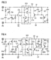
- the control circuit is in FIG. 3 realized by a detector circuit with downstream control transistors TH1 and TL1 as output switching elements.
- the detector circuit includes two subcircuits, one of which drives transistor T1 and the other drives transistor T2.
- each detector subcircuit for transient detection an RC element of the series connection of a capacitance and a resistor which is connected to the lines LV and LB and the corresponding terminals PV and PB.
- Each detector subcircuit of capacitance and resistance forms as RC element a complex voltage divider, at whose center tap the voltage increase of the interference pulse is detected.
- the (complex) resistance of the capacitance low ("low"), so that sets a low or high potential at the output node of the detector circuit depending on the polarity of the RC circuit.
- the node voltage reaches the switching threshold of the detector transistor (TD1 or TD2), it switches on and generates at its output a potential that can drive and switch through the control transistors (TH1 or TL1).
- the output voltages of the switched control transistors cause the pn junction between the emitter and base of T1 and T2 exceeds the switching threshold and turns on the protection circuit.
- the detector subcircuit for driving T1 is made up of the series connection of a capacitor C13 and a resistor R13.
- the connection node of the capacitor C13 and the resistor R13, the transistor TD1 is connected downstream.
- TD1 is formed as a p-channel transistor.
- TD1 controls the output side of the n-channel control transistor TL1.
- TL1 is connected on the output side to the base of T1.
- the resistance of C13 becomes low, so that TD1 turns on and the output of TD1 assumes high potential, in particular VV, and drives TL1.
- the output of TL1 or the base of T1 are thereby set to reference potential VB and T1 turns on.
- the detector subcircuit for driving T2 differs from the detector subcircuit for driving T1 in that the RC series circuit of the capacitive and the resistive device is connected in the opposite direction to the terminals PV and PB.
- the resistor R2 is connected to the terminal PB and the capacitor C2 to the terminal PV.
- connection node of the capacitor C2 and the resistor R2, the transistor TD2 is connected downstream.
- TD is formed as an n-channel transistor.
- TD2 controls the output side of the p-channel control transistor TH1.
- TH1 has its output connected to the base of T2.
- the resistance of C2 becomes low, so that TD2 switches and the output of TD2 becomes low, in particular VB, and can drive TH1 through.
- the output of TH1 and the base of T2 are thereby set to high potential VV and T2 turns on.
- detector circuit may be useful as long as the essential function described above is met.
- the decisive factor is that the transient signal is detected on the one hand, and on the other hand, in normal operation, the thyristor SCR not ignited.
- the time constant of the RC element determines the detection of a transient pulse.
- T2 switches to the conducting state at the same time or almost simultaneously with T1.
- the thyristor SCR becomes conductive and the transient pulse present on the line LV or the connection PV can be derived against the reference potential.
- R3, C3 and R4, C4 determine how long the control circuit remains active or after which time the protection circuit SCR is turned off again. It can thus be ensured that the control signals of the control circuit control the thyristor SCR at least until the transient pulse on the line LV or the terminal PV has decayed with certainty.
- the parallel connection of a further RC element of the capacitor C3 and the resistor R3 is connected between the base terminal of the transistor TL1 and reference potential VB. Between the base terminal of the transistor TH1 and high potential VV, the parallel connection of an RC element of the capacitor C4 and the resistor R4 is connected.
- the time constants of the RC element from the elements C3, R3 and C4, R4 can be set independently of the associated time constant of the RC element of C13, R13 or C2, R2 and determine how long the control circuit remains active and the control signals abut the transistors T1 and T2. As long as TL1 or TH1 remain switched through, you can TL1 and TH1 generate the control currents for the connection of the transistors T1 and T2.
- the time constants R3, C3 and R4, C4 are set so that the control circuit will output the control signals to the protection circuit as long as the transient fault persists.
- the time constants of C3 and R3 or C4 and R4 when the transistors TD1 and TD2 are switched off, the inputs of the control transistors TL1 and TH1 are blocked and the control currents of T1 and T2 are switched off.
- time constants By setting the time constants, different transient pulse shapes can be detected and derived. Furthermore, the time constants of the RC elements can be independently optimized with regard to their function.
- FIG. 4 shows a further embodiment of the invention, which is compared to the embodiment of the FIG. 3 essentially differs in that additional gate driver transistors are used. This makes it possible to improve the switching behavior of the control or trigger transistors TH10 and TL10.
- transistor T11 as a gate driver for TD10 requires reversing the polarity of the detecting RC element so that C10 is connected to VV and R10 is connected to VB.
- the n-channel driver transistor T12 in the output circuit of TD10 drives the p-channel switching transistor TH10, which in turn drives T20.
- the p-channel driver transistor T13 in the output circuit of TD20 drives the n-channel switching transistor TL10, which in turn drives T10.
- control circuit for detecting the transient event and for driving T1 or T2 is constructed from two subcircuits or subcircuits, which are assigned separately to each of the transistors T1 and T2.
- the separate implementation of the subcircuits of the control circuit allows independent dimensioning and optimization of these subcircuits.
- the further embodiment according to FIG. 5 differs from the embodiment of FIG. 4 in that both control transistors TL10 and TH10 with upstream driver transistors T13 and T12 use the same detector circuit.
- T12 serves not only to drive TH10, but also to drive the gate driver transistor T13 and the downstream switching element TL10.
- the elements C10, R10, T11, TD10 and C30, R30 are provided only once in the protection circuit.
- the elements R20, C20, R40, C40, TD20 and T21 of the second detector subcircuit may be omitted.
- the use of single transistors in the control circuit requires no inverters to trigger the protection circuit SCR.
- An optimization of the individual transistors, which are used as switching elements of the control circuit is possible in every manufacturing process of the integrated circuit, in particular in high-voltage processes, but also in standard processes. Thus, even using a high-voltage process as well as low-voltage processes, an optimized protection circuit can be produced.
- the invention is not limited to the use of MOS transistors as switching elements.
- bipolar transistors can be used as switching elements.
- the structure of the protective device in the semiconductor device is the embodiment according to FIG. 6 at.
- a low p-doped well 10 is arranged.
- the well 10 may also be the substrate of the semiconductor.
- an n-doped well 20 is arranged in the tub 10.
- the thyristor of T1 and T2 is embedded in the embodiment using a high-voltage process in the n-well 20.
- the n-well 20 serves to control the high voltages occurring.
- highly doped regions with p- or n-conductivity are arranged, which can be generated in a conventional manner, for example by implantation or diffusion.
- the highly doped n-region 21 and the highly doped p-region 22 can be separately connected to a potential, but they must have the same potential during operation. For this purpose, they are each connected to the high potential VV.
- the heavily doped n-region 23 is connected to the output CTL of the control circuit.
- a p-doped well 30 is arranged in the n-well 20.
- two highly doped p-regions 31 and 33 and a highly doped n-region 32 are arranged. These may be fabricated by implantation or diffusion in a conventional manner similar to the heavily doped regions of the n-well.
- the regions 32 and 33 can be separately connected to a potential, but they must have the same potential during operation. In the example, they are each connected to the reference potential VB.
- the region 31 is connected to the output CTH of the control circuit.
- field plates P11 and P12 are made of polysilicon (typically as a polylayer).
- the field plates serve to control the electric field at the high operating voltages and increase the breakdown voltage of the device. This results in a lower susceptibility of the circuit against false triggering.
- the parasitic thyristor structure with the transistors T1 and T2 is shown in the n- or p-well. Thereafter, the collector of the npn transistor T2 results between the region 21 with a downstream resistor RN of the n-well 20 and the region 23. The base results from the region 31 and the collector of T1 and is connected via the resistor RP of the p-type. Tub 30 connected to reference potential VB. The base of this transistor T2 is connected to the region 31 as a control terminal to which the control signal CTH for turning on and off of the transistor can be applied. The emitter results as area 32.
- the base of the pnp transistor T1 results between the region 21 and the downstream path resistance RN of the n-well 20 and the collector of the transistor T2 and the region 23, to which the signal CTL is applied.
- the collector of T1 results between terminal 33 with downstream track resistance RP of the p-well 30 and the area 31.
- the emitter of the transistor T1 is connected to the area 22.
- the control signal CTL is used to turn on or off the transistor T1.
- the control lines or control signals CTL and CTH are first set to low potential (range 23) or high potential (range 31) to the transistors T1 and T2 turn.
- a base current for the pnp or npn transistor is provided. The base currents turn on the respective transistor and thus ignite the thyristor.
- the protective function between the lines LV and LB is in operation.
- the region 23 is set to high potential via the connection CTL after switching off the control transistor TL1 means of the rail resistor RN and the area 31 via the terminal CTH after switching off the control transistor TH1 by means of the web resistance RP to low potential. This locks the transistors T1 and T2 and thus the thyristor.
Abstract
Description
Die Erfindung betrifft eine Schaltungsanordnung zum Schutz einer integrierten Halbleiterschaltung mit einer Schutzschaltung, die eine Thyristorstruktur enthält und zwischen ein zu schützendes Element und ein Bezugspotential geschaltet ist, und mit einer Steuerschaltung für die Ansteuerung der Schutzschaltung sowie ein entsprechendes Verfahren zum Schutz einer integrierten Halbleiterschaltung.The invention relates to a circuit arrangement for protecting a semiconductor integrated circuit with a protective circuit, which includes a thyristor structure and is connected between a protected element and a reference potential, and with a control circuit for driving the protection circuit and a corresponding method for protecting a semiconductor integrated circuit.
Integrierte Halbleiterschaltungen (ICs) können durch transiente Pulse oder Überspannungen, die über Anschlüsse (Pads) oder direkt in Leitungen eingekoppelt werden, so beschädigt werden, dass sie funktionsunfähig oder gar zerstört werden. Derartige Pulse oder Überspannungen können beispielsweise bei sogenannten elektrostatischen Entladungen (englisch: ESD, Electrostatic Discharge) auftreten. Hohe Spannungen und hohe Ströme, verbunden mit transienten bzw. ESD-Störungen, bewirken das Auftreten hoher störender Leistungen.Integrated semiconductor (IC) circuits can be damaged by transient pulses or overvoltages that are coupled via leads (pads) or directly into lines, so that they become inoperable or even destroyed. Such pulses or overvoltages can occur, for example, in so-called electrostatic discharges (English: ESD, Electrostatic Discharge). High voltages and high currents, combined with transient or ESD disturbances, cause the occurrence of high disturbing power.
Auch in vielen Anwendungsgebieten, z.B. der Automobiltechnik, kann ein derartiger Puls (z.B. Burst) auftreten. In der Automobiltechnik beispielsweise besteht das Erfordernis, derartige Schaltungen, die im Hochvoltbereich bis 90 Volt oder darüber funktionieren müssen, auch für deutlich höhere Störpuls-Pegel auszulegen.Also in many fields of application, e.g. In automotive engineering, such a pulse (e.g., burst) may occur. In automotive engineering, for example, there is a need to design such circuits, which must operate in the high-voltage range up to 90 volts or above, also for significantly higher interference pulse levels.
Für Hochvoltanwendungen, die mit Hochvoltprozessen hergestellt sind, werden gewöhnlich Schutzeinrichtungen vorgesehen, die von einem elektrischen Durchbruch ausgelöst bzw. getriggert werden. Die Durchbruchspannungen müssen deutlich oberhalb der maximal zulässigen Betriebsspannungen der zu schützenden Anwendungsschaltung liegen. Nur dann kann eine ungestörte Funktionalität der integrierten Schaltung garantiert werden. Im Fehlerfall, z.B. bei Vorliegen einer unzulässig hohen Spannung, wird diese Überspannung durch die Schutzschaltung gegen Bezugspotential bzw. Masse abgeleitet und so nachfolgende Baugruppen vor der hohen Spannung geschützt.For high voltage applications, which are manufactured with high-voltage processes, usually protective devices are provided, which are triggered or triggered by an electrical breakdown. The breakdown voltages must be well above the maximum permissible operating voltages of the application circuit to be protected. Only then can an undisturbed functionality of the integrated circuit be guaranteed. In the event of a fault, for example in the presence of an impermissibly high voltage, this overvoltage is derived by the protective circuit against reference potential or ground and so protects subsequent modules from the high voltage.
Eine Alternative für solche durchbruch-basierten Schutzkonzepte ist eine aktive Schaltung zum Schutz einer integrierten Schaltung, bestehend aus einer Kombination einer aktiven Triggerschaltung mit einer bekannten Schutzeinrichtung wie einem Thyristor bzw. einem bipolaren oder MOS-Schutztransistor.An alternative for such breakthrough-based protection concepts is an active circuit for protecting an integrated circuit, consisting of a combination of an active trigger circuit with a known protection device such as a thyristor or a bipolar or MOS protection transistor.
Aktive Schaltungen zum Schutz des ICs werden oft durch den Anstieg des transienten Signals getriggert. Dabei wird der Signalanstieg pro Zeiteinheit detektiert und über eine Ansteuerschaltung ein Schutztransistor oder eine Schutzschaltung durchgeschaltet.Active circuits to protect the IC are often triggered by the rise of the transient signal. In this case, the signal rise per unit of time is detected and a protective transistor or a protective circuit is switched through via a drive circuit.
Im Fehlerfall kann die Schutzschaltung demnach als aktiv getriggerter Überspannungs- oder Überstromableiter verstanden werden. Im Fehlerfall ist eine schnelle Durchsteuerung der Schutzschaltung notwendig.In the event of a fault, the protective circuit can therefore be understood as an actively triggered overvoltage or overcurrent arrester. In the event of a fault, rapid control of the protection circuit is necessary.
Geringe Einschaltzeiten und eine präzise Einschaltschwelle der Schutzschaltung für den integrierten Schaltkreis sowie deren Schutzwirkung bei unterschiedlichen Formen von Störpulsen sind bedeutende Aspekte der Produktspezifikation und stellen einen Wettbewerbsvorteil dar.Low switch-on times and a precise turn-on threshold of the protection circuit for the integrated circuit as well as their protective effect with different forms of interference pulses are significant aspects of the product specification and represent a competitive advantage.
Aus der
Ein weiteres Dokument XP-002346581, IEEE TRANSACTIONS ON DEVICE AND MATERIALS RELIABILITY, VOL 3, NO 3, SEPTEMBER 2003: SCC DEVICE WITH DOUBLE TRIGGERED TECHNIQUE FOR ON-CHIP ESD PROTECTION IN SUB QUARTER MICRON SLICIDED CMOS PROCESSES, ist bekannt.Another document XP-002346581, IEEE TRANSACTIONS ON DEVICE AND MATERIALS RELIABILITY, VOL 3, NO 3, SEPTEMBER 2003: SCC DEVICE WITH DOUBLE TRIGGERED TECHNIQUE FOR ON-CHIP ESD PROTECTION IN SUB QUARTER MICRON SLICIDED CMOS PROCESSES, is known.
Der Erfindung liegt die Aufgabe zugrunde, eine Schaltungsanordnung und ein Verfahren zum Schutz von integrierten Halbleiterschaltungen anzugeben, die ein verbessertes Verhalten ermöglichen. Weiterhin sollen eine Schaltungsanordnung und ein Verfahren angegeben werden, die insbesondere auch für Hochvoltprozesse bzw. für Hochvoltanwendungen geeignet sind.The invention has for its object to provide a circuit arrangement and a method for protecting semiconductor integrated circuits, which allow improved performance. Furthermore, a circuit arrangement and a method are to be specified, which are particularly suitable for high-voltage processes or for high-voltage applications.
Diese Aufgabe löst die Erfindung mit den Merkmalen des Patentanspruchs 1.This object is achieved by the invention with the features of
Die Erfindung hat den Vorteil, dass die Schaltungsanordnung als aktiv getriggerte Schutzschaltung und das entsprechende Verfahren ein schnelles Durchschalten der Thyristorstruktur ermöglichen. Ferner lässt sich die Erfindung in Hochvoltanwendungen, die unter Verwendung von Hochvoltprozessen hergestellt sind, integrieren.The invention has the advantage that the circuit arrangement as an actively triggered protection circuit and the corresponding Procedure to enable a quick turn on the thyristor structure. Further, the invention can be integrated in high voltage applications fabricated using high voltage processes.
Vorteilhafte Ausgestaltungen und Weiterbildungen der Erfindung sind Gegenstand der abhängigen Patentansprüche.Advantageous embodiments and modifications of the invention are the subject of the dependent claims.
Die Erfindung wird im folgenden anhand von Ausführungsbeispielen im Zusammenhang mit den Figuren näher erläutert. Gleiche oder gleichwirkende Elemente sind in den Figuren mit gleichen Bezugszeichen versehen.The invention will be explained in more detail below with reference to exemplary embodiments in conjunction with the figures. The same or equivalent elements are provided in the figures with the same reference numerals.
Es zeigen:
Figur 1- eine schematisch dargestellte Schaltungsanordnung mit Schutzschaltung und Steuer- bzw. Triggerschaltung
- Figur 2
- eine zweite schematisch dargestellte Schaltungsanordnung mit Schutzschaltung und Triggerschaltung,
- Figur 3
- eine dritte schematisch dargestellte Schaltungsanordnung mit Schutzschaltung und Triggerschaltung,
- Figur 4
- eine vierte schematisch dargestellte Schaltungsanordnung mit Schutzschaltung und Triggerschaltung,
- Figur 5
- eine weitere schematisch dargestellte Schaltungsanordnung mit Schutzschaltung und Triggerschaltung und
- Figur 6
- einen schematischen Querschnitt einer Struktur zur Realisierung des Thyristors in einem Hochvoltprozess.
- FIG. 1
- a schematically illustrated circuit arrangement with protection circuit and control or trigger circuit
- FIG. 2
- a second schematically illustrated circuit arrangement with protection circuit and trigger circuit,
- FIG. 3
- a third schematically illustrated circuit arrangement with protection circuit and trigger circuit,
- FIG. 4
- a fourth schematically illustrated circuit arrangement with protection circuit and trigger circuit,
- FIG. 5
- a further schematically illustrated circuit arrangement with protection circuit and trigger circuit and
- FIG. 6
- a schematic cross section of a structure for the realization of the thyristor in a high-voltage process.
In
Die eigentliche Aufgabe der Ableitung von Störpulsen bzw. Überspannungen erfüllt die Schutzschaltung PC, die in allen Ausführungsbeispielen als SCR bezeichnet ist. Gesteuert bzw. getriggert wird die Schutzschaltung PC bzw. SCR von einer Steuerschaltung TC, die eingangsseitig mit den Anschlüssen PV und PB verbunden ist. Die Steuerschaltung TC enthält eine Detektorschaltung, die in der Lage ist, die an dem Anschluss PV bzw. der Leitung auftretenden transienten Pulse zu erkennen und Steuersignale für die Schutzschaltung PC bzw. SCR zu erzeugen.The actual task of deriving interference pulses or overvoltages fulfills the protective circuit PC, which is designated in all exemplary embodiments as SCR. The protection circuit PC or SCR is controlled or triggered by a control circuit TC, which is connected on the input side to the terminals PV and PB. The control circuit TC includes a detector circuit capable of detecting the transient pulses appearing at the terminal PV and the line and generating control signals for the protection circuit PC and SCR, respectively.
Die Steuerschaltung TC erzeugt mehrere Steuersignale, die jeweils ein aktives Element der Schutzschaltung PC bzw. SCR ansteuern. In
Im typischen Anwendungsfall der
Das Durchschalten der Schutzschaltung PC bzw. SCR mittels Steuersignalen für die aktiven Elemente der Schutzschaltung, die in ihrer Zusammenschaltung die niederohmige Verbindung zwischen der Leitung LV und der Leitung LB herstellen müssen, wird so gezielt eingeleitet. Dadurch ist es möglich, die Schutzschaltung PC bzw. SCR präzise und schnell in den durchgeschalteten Zustand zu führen. Dies führt zu einem verbesserten Ansprechverhalten der Schutzschaltung und damit zu einem besseren Schutz der integrierten Halbleiterschaltung, die in der
Gemäß
Die Steuerschaltung ist in der
Die Detektorschaltung aus Kapazität C1 und Widerstand R1 bildet als RC-Glied einen komplexen Spannungsteiler, an dessen Mittelabgriff der Spannungsanstieg des Störpulses erfasst wird. Im Fehlerfall eines transienten Pulses wird die Kapazität C1 niederohmig, sodass sich am Ausgangspunkt der Detektorschaltung ein hohes Potential einstellt. Sobald die Spannung die Schaltschwelle des Inverters I1 erreicht, schaltet dessen Ausgangssignal CTL auf niedriges Potential, so dass der pn-Übergang zwischen Emitter und Basis von T1 die Schaltschwelle überschreitet und T1 durchschaltet.The detector circuit of capacitance C1 and resistor R1 forms as RC element a complex voltage divider, at whose center tap the voltage increase of the interference pulse is detected. In the event of an error of a transient pulse, the capacitance C1 becomes low, so that at the starting point of the detector circuit sets a high potential. As soon as the voltage reaches the switching threshold of the inverter I1, its output signal CTL switches to low potential, so that the pn junction between emitter and base of T1 exceeds the switching threshold and T1 turns on.
Andererseits liegen parallel zu I1 die hintereinander geschalteten Inverter I2 und I3, die das am Abgriffsknoten der Detektorschaltung detektierte Spannungssignal in ein definiertes Steuersignal CTH zur Ansteuerung des npn-Transistors T2 umsetzen. Somit schaltet T2 nahezu zeitgleich mit T1 in den leitenden Zustand über. Damit wird der Thyristor SCR leitend und der auf der Leitung LV bzw. dem Anschluss PV anliegende transiente Puls kann gegen Bezugspotential abgeleitet werden.On the other hand, the inverters I2 and I3, which are connected in series, are connected in parallel with I1 and convert the voltage signal detected at the tap node of the detector circuit into a defined control signal CTH for driving the NPN transistor T2. Thus, T2 switches to the conducting state almost at the same time as T1. Thus, the thyristor SCR becomes conductive and the transient pulse present on the line LV or the connection PV can be derived against the reference potential.
Das Beispiel gemäß
Im Fehlerfall eines transienten Pulses wird die Kapazität C11 niederohmig, so dass sich am Ausgangspunkt der Detektorschaltung ein niedriges Potential einstellt. Der Inverter I6 setzt dieses niedrige Potential in eine zur Durchsteuerung des Transistors T2 erforderliche Spannung bzw. einen entsprechenden Steuerstrom um. Andererseits formen die in Serie geschalteten Inverter I4 und 15 die Ausgangsspannung an der Kapazität C11 in ein Steuersignal niedrigen Potentials bzw. einen entsprechenden Strom um, so dass der Transistor T1 durchschaltet.In the event of an error of a transient pulse, the capacitance C11 becomes low, so that at the starting point of the detector circuit set a low potential. The inverter I6 converts this low potential into a voltage required for the control of the transistor T2 or a corresponding control current. On the other hand, the series-connected inverters I4 and 15 convert the output voltage at the capacitor C11 into a control signal of low potential or a corresponding current, so that the transistor T1 turns on.
Die Detektorschaltung ist in den Beispielen der
Maßgebend ist, dass das transiente Signal einerseits erkannt wird und andererseits im Normalbetrieb der Thyristor SCR nicht gezündet wird. Die Zeitkonstante des RC-Gliedes bestimmt einerseits das Erkennen eines transienten Pulses als auch andererseits die Zeit, während der die Detektorschaltung aktiv ist. Ein Puls wird erkannt und detektiert, so lange die Anstiegszeit der transienten Störung kleiner ist als die Zeitkonstante des RC-Gliedes. Andererseits bestimmt die Zeitkonstante nach Abklingen des Pulses die Zeit, nach der die Detektorschaltung inaktiv wird und abschaltet bzw. wieder in den Normalbetrieb zurückkehrt.The decisive factor is that the transient signal is detected on the one hand and on the other hand, the thyristor SCR is not ignited in normal operation. The time constant of the RC element determines on the one hand the detection of a transient pulse and on the other hand the time during which the detector circuit is active. A pulse is detected and detected as long as the rise time of the transient disturbance is less than the time constant of the RC element. On the other hand, the time constant determined by the decay of the pulse, the time after which the detector circuit is inactive and shuts down or returns to normal operation.
Dazu wird in den Bespielen der
Bei jeweils einer kleinen Kapazität des RC-Gliedes, beispielsweise realisiert als Gateoxidkapazität, wird der Widerstand dieser Kapazität bei transienten Vorgängen niedrig, so dass im Beispiel der
Die Schaltungsanordnungen der
Im Vergleich des Beispiels nach
Dem Ausgang des ersten RC-Gliedes aus R12 und C12 ist als Element der Zusatzschaltung ein Inverter I10 nachgeschaltet, der einen PMOS-Transistor P10 ansteuert. Ausgangsseitig ist dieser Transistor einerseits mit der Spannung führenden Leitung LV und andererseits mit den Eingängen der Inverter I20 und I30 verbunden. An dem letzteren Verbindungspunkt ist weiterhin die Parallelschaltung eines zweiten RC-Gliedes aus der Kapazität C21 und dem Widerstand R21 angeschlossen, die mit ihrem anderen Anschluss jeweils an dem Bezugspotential VB bzw. der Leitung LB angeschlossen sind.The output of the first RC element of R12 and C12, an inverter I10 is connected as an element of the additional circuit, which drives a PMOS transistor P10. On the output side, this transistor is connected on the one hand to the voltage-carrying line LV and on the other hand to the inputs of the inverters I20 and I30. At the latter connection point, the parallel connection of a second RC element of the capacitor C21 and the resistor R21 is also connected, which are connected with their other terminal respectively to the reference potential VB and the line LB.
Bei einer transienten Störung auf der Leitung LV oder dem Anschluss PV wird diese durch das erste RC-Glied erkannt. Der Ausgang dieses ersten RC-Gliedes, das den Inverter I10 ansteuert, nimmt bei einem schnellen Pulsanstieg durch die dann niederohmige Kapazität C12 hohes Potential an, sodass der Inverter I10 ausgangsseitig auf niedriges Potential gebracht wird. Wie in den Beispielen der
Mit dem dann niederohmigen Ausgang des Inverters I10 wird der PMOS-Transistor P10 durchgesteuert, dessen Ausgang die Invertereingänge der Inverter 120 und I30 auf hohes Potential legt. Wie schon anhand des Beispiels der
Die Zeitkonstante des zweiten RC-Gliedes aus den Elementen C21 und R21 kann unabhängig von der Zeitkonstante des ersten RC-Gliedes eingestellt werden und bestimmt in dieser Situation, wie lange die Steuerschaltung aktiv bleibt und Steuersignale an die Transistoren T1 und T2 erzeugt. Solange P10 durchgeschaltet bleibt, sind die Inverter I20, I30 und I40 in der Lage, die Steuerströme für die Durchschaltung der Transistoren T1 und T2 zu erzeugen. Sobald P10 abschaltet, z.B. weil sich der transiente Puls verflacht und die Zeitkonstante des ersten RC-Gliedes kürzer als die Spannungsänderungen auf der Leitung LV werden, wird der Verbindungsknoten der Eingänge der Inverter I20 und I30 mit dem zweiten RC-Glied über dieses RC-Glied und dessen Zeitkonstante gegen Bezugspotential entladen. Typischerweise wird die Zeitkonstante des zweiten RC-Gliedes so eingestellt, dass die Steuerschaltung die Steuersignale an den Thyristor so lange abgibt, wie die transiente Störung andauert. Das bedeutet, dass die Zeitkonstante des zweiten RC-Gliedes größer ist als die Zeitkonstante des ersten RC-Gliedes. Auf diese Weise können mittels des ersten und des zweiten RC-Gliedes unterschiedliche transiente Pulsformen erfasst und abgeleitet werden. Weiterhin können die Zeitkonstanten der beiden RC-Glieder unabhängig voneinander im Hinblick auf ihre Funktion optimiert werden.The time constant of the second RC element of the elements C21 and R21 can be set independently of the time constant of the first RC element and determines in this situation how long the control circuit remains active and generates control signals to the transistors T1 and T2. As long as P10 remains turned on, inverters I20, I30 and I40 are capable of generating the control currents for the turn-on of transistors T1 and T2. As soon as P10 switches off, eg because the transient pulse flattens out and the time constant of the first RC element becomes shorter than the voltage changes on the line LV, the connection node of the inputs of the inverters I20 and I30 with the second RC element becomes via this RC element and discharge its time constant against reference potential. Typically, the time constant of the second RC element is adjusted so that the control circuit outputs the control signals to the thyristor as long as the transient fault persists. This means that the time constant of the second RC element is greater than the time constant of the first RC element. In this way, different transient pulse shapes can be detected and derived by means of the first and the second RC element. Furthermore, the time constants of the two RC elements can be optimized independently of each other with regard to their function.
Selbstverständlich kann das Ausführungsbeispiel mit einem zweiten RC-Glied auch an das erste Ausführungsbeispiel nach
Die vorstehend beschriebenen aktiv getriggerten Schutzschaltungskonzepte machen von Invertern Gebrauch. Die Inverter liefern die Spannungen bzw. Ströme mit den notwendigen kurzen Signalanstiegszeiten, um die eigentliche Schutzschaltung zu triggern.The active triggered protection circuit concepts described above make use of inverters. The inverters provide the voltages or currents with the necessary short signal rise times to trigger the actual protection circuit.
Der Einsatz von Invertern in Hochvoltanwendungen ist wiederum nicht völlig unproblematisch. Hochvoltbauelemente, die unter Verwendung von Hochvoltprozessen hergestellt sind, weisen oft unsymmetrische Betriebsparameter bzw. Betriebsbedingungen auf, die in der Natur des Hochvoltprozesses, insbesondere den mehrfachen Isolationswannen, begründet sind. Zum Beispiel kann die maximal zulässige Drain-Source-Spannung eines MOS-Transistors beträchtlich höher sein als die entsprechende maximal zulässige Gate-Bulk-Spannung. Deshalb können bestimmte Bauelement-Konfigurationen, wie z.B. Standard-Inverter, nicht für die möglichen Spannungsbereiche hergestellt werden.The use of inverters in high-voltage applications, in turn, is not completely unproblematic. High-voltage components, which are manufactured using high-voltage processes, often have asymmetrical operating parameters or operating conditions, which are due to the nature of the high-voltage process, in particular the multiple insulation wells. For example, the maximum allowable drain-source voltage of a MOS transistor may be considerably higher than the corresponding maximum allowable gate bulk voltage. Therefore, certain device configurations, such as e.g. Standard inverters, not manufactured for the possible voltage ranges.
Gemäß dem ersten Ausführungsbeispiel der Erfindung ist die Steuerschaltung in
Jede Detektorteilschaltung aus Kapazität und Widerstand bildet als RC-Glied einen komplexen Spannungsteiler, an dessen Mittelabgriff der Spannungsanstieg des Störpulses erfasst wird. Im Fehlerfall eines transienten Pulses wird, wie beschrieben, der (komplexe) Widerstand der Kapazität niedrig ("niederohmig"), so dass sich am Ausgangsknoten der Detektorschaltung je nach Polung der RC-Schaltung ein niedriges bzw. hohes Potential einstellt. Sobald die Knotenspannung die Schaltschwelle des Detektortransistors (TD1 bzw. TD2) erreicht, schaltet dieser durch und erzeugt an seinem Ausgang ein Potential, das die Steuertransistoren (TH1 bzw. TL1) ansteuern und durchschalten kann. Die Ausgangsspannungen der geschalteten Steuertransistoren bewirken, dass der pn-Übergang zwischen Emitter und Basis von T1 bzw. T2 die Schaltschwelle überschreitet und die Schutzschaltung durchschaltet.Each detector subcircuit of capacitance and resistance forms as RC element a complex voltage divider, at whose center tap the voltage increase of the interference pulse is detected. In case of failure of a transient pulse, as described, the (complex) resistance of the capacitance low ("low"), so that sets a low or high potential at the output node of the detector circuit depending on the polarity of the RC circuit. As soon as the node voltage reaches the switching threshold of the detector transistor (TD1 or TD2), it switches on and generates at its output a potential that can drive and switch through the control transistors (TH1 or TL1). The output voltages of the switched control transistors cause the pn junction between the emitter and base of T1 and T2 exceeds the switching threshold and turns on the protection circuit.
Die Detektorteilschaltung für die Ansteuerung von T1 ist aus der Serienschaltung einer Kapazität C13 und eines Widerstands R13 ausgeführt. Dem Verbindungsknoten der Kapazität C13 und des Widerstandes R13 ist der Transistor TD1 nachgeschaltet. TD1 ist als p-Kanal-Transistor ausgebildet. TD1 steuert ausgangsseitig den n-Kanal-Steuertransistor TL1 an. TL1 ist ausgangsseitig mit der Basis von T1 verbunden.The detector subcircuit for driving T1 is made up of the series connection of a capacitor C13 and a resistor R13. The connection node of the capacitor C13 and the resistor R13, the transistor TD1 is connected downstream. TD1 is formed as a p-channel transistor. TD1 controls the output side of the n-channel control transistor TL1. TL1 is connected on the output side to the base of T1.
Im Fall einer transienten Störung wird der Widerstand von C13 niedrig, so dass TD1 durchschaltet und der Ausgang von TD1 hohes Potential, insbesondere VV, annimmt und TL1 durchsteuert. Der Ausgang von TL1 bzw. die Basis von T1 werden dadurch auf Bezugspotential VB gelegt und T1 schaltet durch.In the case of a transient disturbance, the resistance of C13 becomes low, so that TD1 turns on and the output of TD1 assumes high potential, in particular VV, and drives TL1. The output of TL1 or the base of T1 are thereby set to reference potential VB and T1 turns on.
Die Detektorteilschaltung für die Ansteuerung von T2 unterscheidet sich von der Detektorteilschaltung für die Ansteuerung von T1 dadurch, dass die RC-Serienschaltung aus dem kapazitiven und dem resistiven Bauelement in umgedrehter Richtung mit den Anschlüssen PV und PB verbunden ist. Dabei liegt der Widerstand R2 am Anschluss PB und die Kapazität C2 am Anschluss PV. Somit drehen sich die Spannungsverhältnisse am Ausgang der Detektorschaltung, nämlich dem Verbindungspunkt von R2 und C2 um, sodass auch die Ansteuerung des Transistors T2 anders erfolgen muss.The detector subcircuit for driving T2 differs from the detector subcircuit for driving T1 in that the RC series circuit of the capacitive and the resistive device is connected in the opposite direction to the terminals PV and PB. In this case, the resistor R2 is connected to the terminal PB and the capacitor C2 to the terminal PV. Thus, the voltage conditions at the output of the detector circuit, namely the connection point of R2 and C2, so that the driving of the transistor T2 must be done differently.
Dem Verbindungsknoten der Kapazität C2 und des Widerstandes R2 ist der Transistor TD2 nachgeschaltet. TD ist als n-Kanal-Transistor ausgebildet. TD2 steuert ausgangsseitig den p-Kanal-Steuertransistor TH1 an. TH1 ist ausgangsseitig mit der Basis von T2 verbunden.The connection node of the capacitor C2 and the resistor R2, the transistor TD2 is connected downstream. TD is formed as an n-channel transistor. TD2 controls the output side of the p-channel control transistor TH1. TH1 has its output connected to the base of T2.
Im Fall einer transienten Störung wird der Widerstand von C2 niedrig, so dass TD2 schaltet und der Ausgang von TD2 niedriges Potential, insbesondere VB, annimmt und TH1 durchsteuern kann. Der Ausgang von TH1 bzw. die Basis von T2 werden dadurch auf hohes Potential VV gelegt und T2 schaltet durch.In the case of a transient disturbance, the resistance of C2 becomes low, so that TD2 switches and the output of TD2 becomes low, in particular VB, and can drive TH1 through. The output of TH1 and the base of T2 are thereby set to high potential VV and T2 turns on.
Es können auch andere Ausführungsformen der Detektorschaltung zweckmäßig sein, so lange die wesentliche vorstehend beschrieben Funktion erfüllt wird.Other embodiments of the detector circuit may be useful as long as the essential function described above is met.
Maßgebend ist, dass das transiente Signal einerseits erkannt wird und andererseits im Normalbetrieb der Thyristor SCR nicht gezündet wird. Die Zeitkonstante des RC-Gliedes bestimmt das Erkennen eines transienten Pulses.The decisive factor is that the transient signal is detected on the one hand, and on the other hand, in normal operation, the thyristor SCR not ignited. The time constant of the RC element determines the detection of a transient pulse.
Dann schaltet T2 zeitgleich oder nahezu zeitgleich mit T1 in den leitenden Zustand über. Damit wird der Thyristor SCR leitend und der auf der Leitung LV bzw. dem Anschluss PV anliegende transiente Puls kann gegen Bezugspotential abgeleitet werden. Selbstverständlich kann man auch unterschiedliche Zeitkonstanten einstellen, wenn sich diese Notwendigkeit ergeben sollte.Then T2 switches to the conducting state at the same time or almost simultaneously with T1. Thus, the thyristor SCR becomes conductive and the transient pulse present on the line LV or the connection PV can be derived against the reference potential. Of course you can also set different time constants, if this need should arise.
Die in
So ist zwischen dem Basisanschluss des Transistors TL1 und Bezugpotential VB die Parallelschaltung eines weiteren RC-Gliedes aus der Kapazität C3 und dem Widerstand R3 angeschlossen. Zwischen dem Basisanschluss des Transistors TH1 und hohem Potential VV ist die Parallelschaltung eines RC-Gliedes aus der Kapazität C4 und dem Widerstand R4 angeschlossen.Thus, the parallel connection of a further RC element of the capacitor C3 and the resistor R3 is connected between the base terminal of the transistor TL1 and reference potential VB. Between the base terminal of the transistor TH1 and high potential VV, the parallel connection of an RC element of the capacitor C4 and the resistor R4 is connected.
Die Zeitkonstanten des RC-Gliedes aus den Elementen C3, R3 bzw. C4, R4 können unabhängig von der zugeordneten Zeitkonstante des RC-Gliedes aus C13, R13 bzw. C2, R2 eingestellt werden und bestimmen, wie lange die Steuerschaltung aktiv bleibt und die Steuersignale an den Transistoren T1 und T2 anliegen. Solange TL1 bzw. TH1 durchgeschaltet bleiben, können TL1 bzw. TH1 die Steuerströme für die Durchschaltung der Transistoren T1 und T2 erzeugen.The time constants of the RC element from the elements C3, R3 and C4, R4 can be set independently of the associated time constant of the RC element of C13, R13 or C2, R2 and determine how long the control circuit remains active and the control signals abut the transistors T1 and T2. As long as TL1 or TH1 remain switched through, you can TL1 and TH1 generate the control currents for the connection of the transistors T1 and T2.
Sobald sich der transiente Puls verflacht und die Zeitkonstante der RC-Glieder aus C13, R13 bzw. C2, R2 kürzer als die Spannungsänderungen auf der Leitung LV werden, werden die Eingänge von TD1 bzw. TD2 über diese RC-Glieder und ihre Zeitkonstanten gegen hohes Potential bzw. Bezugspotential gelegt. TD1 und TD2 schalten ab.As soon as the transient pulse flattens out and the time constants of the RC elements of C13, R13 or C2, R2 become shorter than the voltage changes on the line LV, the inputs of TD1 or TD2 become high over these RC elements and their time constants Potential or reference potential laid. TD1 and TD2 switch off.
Typischerweise werden die Zeitkonstanten R3, C3 und R4, C4 so eingestellt, dass die Steuerschaltung die Steuersignale an die Schutzschaltung so lange abgibt, wie die transiente Störung andauert. Nach Maßgabe der Zeitkonstanten von C3 und R3 bzw. C4 und R4 werden bei abgeschalteten Transistoren TD1 bzw. TD2 die Eingänge der Steuertransistoren TL1 bzw. TH1 gesperrt und die Steuerströme von T1 und T2 werden abgeschaltet.Typically, the time constants R3, C3 and R4, C4 are set so that the control circuit will output the control signals to the protection circuit as long as the transient fault persists. In accordance with the time constants of C3 and R3 or C4 and R4, when the transistors TD1 and TD2 are switched off, the inputs of the control transistors TL1 and TH1 are blocked and the control currents of T1 and T2 are switched off.
Über die Einstellung der Zeitkonstanten können unterschiedliche transiente Pulsformen erfasst und abgeleitet werden. Weiterhin können die Zeitkonstanten der RC-Glieder unabhängig voneinander im Hinblick auf ihre Funktion optimiert werden.By setting the time constants, different transient pulse shapes can be detected and derived. Furthermore, the time constants of the RC elements can be independently optimized with regard to their function.
Durch den Einsatz der Gatetreiber-Transistoren ist gegenüber
Die Ausführungsbeispiele der
Das weitere Ausführungsbeispiel gemäß
Bei dem Ausführungsbeispiel gemäß
Gemäß dieser Ausführungsform der Erfindung werden durch den Einsatz von Einzeltransistoren in der Steuerschaltung keine Inverter benötigt, um die Schutzschaltung SCR zu triggern. Eine Optimierung der Einzeltransistoren, die als Schaltelemente der Steuerschaltung eingesetzt werden, ist bei jedem Herstellprozess der integrierten Schaltung, insbesondere bei Hochvoltprozessen, aber auch bei Standardprozessen, möglich. Somit kann auch unter Verwendung eines Hochvoltprozesses wie auch bei Niedervoltprozessen eine optimierte Schutzschaltung hergestellt werden.According to this embodiment of the invention, the use of single transistors in the control circuit requires no inverters to trigger the protection circuit SCR. An optimization of the individual transistors, which are used as switching elements of the control circuit, is possible in every manufacturing process of the integrated circuit, in particular in high-voltage processes, but also in standard processes. Thus, even using a high-voltage process as well as low-voltage processes, an optimized protection circuit can be produced.
Selbstverständlich ist die Erfindung nicht auf die Verwendung von MOS-Transistoren als Schaltelemente beschränkt. Ebenso können bipolare Transistoren als Schaltelemente eingesetzt werden.Of course, the invention is not limited to the use of MOS transistors as switching elements. Likewise, bipolar transistors can be used as switching elements.
Die Struktur der Schutzanordnung im Halbleiterbauelement gibt das Ausführungsbeispiel gemäß
In der Wanne 20 sind hochdotierte Bereiche mit p- bzw. n-Leitfähigkeit angeordnet, die in üblicher Weise beispielsweise durch Implantation oder Diffusion erzeugt werden können. Der hochdotierte n-Bereich 21 sowie der hochdotierte p-Bereich 22 können separat an ein Potential gelegt werden, jedoch müssen sie im Betrieb das gleiche Potential aufweisen. Dazu sind sie jeweils mit dem hohen Potential VV verbunden. Der hochdotierte n-Bereich 23 ist mit dem Ausgang CTL der Steuerschaltung verbunden.In the well 20 highly doped regions with p- or n-conductivity are arranged, which can be generated in a conventional manner, for example by implantation or diffusion. The highly doped n-
Ebenfalls in der n-Wanne 20 ist eine p-dotierte Wanne 30 angeordnet. In dieser Wanne 30 sind zwei hochdotierte p-Bereiche 31 und 33 sowie ein hochdotierter n-Bereich 32 angeordnet. Diese können in ähnlicher Weise wie die hochdotierten Bereiche der n-Wanne durch Implantation oder Diffusion in herkömmlicher Weise hergestellt sein. Die Bereiche 32 und 33 können separat an ein Potential gelegt werden, jedoch müssen sie im Betrieb das gleiche Potential aufweisen. Dazu sind sie im Beispiel jeweils mit dem Bezugspotential VB verbunden. Der Bereich 31 ist mit dem Ausgang CTH der Steuerschaltung verbunden.Also in the n-well 20, a p-doped
Oberhalb der Grenzbereiche der n-Wanne 20 und der p-Wanne 30 sind Feldplatten P11 und P12 aus Polysilizium (typischerweise als Polyl-Schicht) ausgebildet. Die Feldplatten dienen zur Steuerung des elektrischen Feldes bei den hohen Betriebsspannungen und erhöhen die Durchbruchspannung der Anordnung. Dadurch ergibt sich eine geringere Anfälligkeit der Schaltung gegen eine falsche Triggerung.Above the boundary regions of the n-well 20 and the p-well 30, field plates P11 and P12 are made of polysilicon (typically as a polylayer). The field plates serve to control the electric field at the high operating voltages and increase the breakdown voltage of the device. This results in a lower susceptibility of the circuit against false triggering.
Die parasitäre Thyristorstruktur mit den Transistoren T1 und T2 ist in die n- bzw. p-Wanne eingezeichnet. Danach ergibt sich der Kollektor des npn-Transistors T2 zwischen dem Bereich 21 mit nachgeschaltetem Widerstand RN der n-Wanne 20 und dem Bereich 23. Die Basis ergibt sich aus dem Bereich 31 sowie dem Kollektor von T1 und ist über den Widerstand RP der p-Wanne 30 mit Bezugspotential VB verbunden. Die Basis dieses Transistors T2 ist mit dem Bereich 31 als Steueranschluss verbunden, an den das Steuersignal CTH zum Ein- und Ausschalten des Transistors angelegt werden kann. Der Emitter ergibt sich als Bereich 32.The parasitic thyristor structure with the transistors T1 and T2 is shown in the n- or p-well. Thereafter, the collector of the npn transistor T2 results between the
Die Basis des pnp-Transistors T1 ergibt sich zwischen dem Bereich 21 und dem nachgeschalteten Bahnwiderstand RN der n-Wanne 20 sowie dem Kollektor des Transistors T2 bzw. dem Bereich 23, an dem das Signal CTL anliegt. Der Kollektor von T1 ergibt sich zwischen Anschluss 33 mit nachgeschaltetem Bahnwiderstand RP der p-Wanne 30 und dem Bereich 31. Der Emitter des Transistors T1 ist mit dem Bereich 22 verbunden. Das Steuersignal CTL dient zum Ein- bzw. Ausschalten des Transistors T1.The base of the pnp transistor T1 results between the
Die Steuerleitungen bzw. Steuersignale CTL bzw. CTH werden zunächst auf niedriges Potential (Bereich 23) bzw. hohes Potential (Bereich 31) gelegt, um die Transistoren T1 und T2 einzuschalten. Dabei wird jeweils ein Basisstrom für den pnp- bzw. npn-Transistor bereitgestellt. Die Basisströme schalten den jeweiligen Transistor ein und zünden somit den Thyristor. Damit ist die Schutzfunktion zwischen den Leitungen LV und LB in Betrieb.The control lines or control signals CTL and CTH are first set to low potential (range 23) or high potential (range 31) to the transistors T1 and T2 turn. In each case, a base current for the pnp or npn transistor is provided. The base currents turn on the respective transistor and thus ignite the thyristor. Thus, the protective function between the lines LV and LB is in operation.
Zum Ausschalten des Thyristors wird der Bereich 23 über den Anschluss CTL nach Abschalten des Steuertransistors TL1 mittels des Bahnwiderstands RN an hohes Potential gelegt und der Bereich 31 über den Anschluss CTH nach Abschalten des Steuertransistors TH1 mittels des Bahnwiderstands RP an niedriges Potential. Damit sperren die Transistoren T1 und T2 und damit den Thyristor.To turn off the thyristor, the region 23 is set to high potential via the connection CTL after switching off the control transistor TL1 means of the rail resistor RN and the
Claims (8)
- A circuit arrangement for protecting an integrated semiconductor circuit comprising- a protection circuit (PC; SCR) which comprises a thyristor structure (T1, T2; T10, T20) with two active elements and is connected between an element to be protected (VV) and a reference potential (VB), and- a control circuit (TC; R2, C2, TD2, TH1, R13, C13, TD1, TL1) which is designed to drive the protection circuit and is connected in parallel with the protection circuit between the element to be protected and the reference potential (VB), wherein- the control circuit comprises a detector circuit (R2, C2, TD2, R13, C13, TD1) and two switching elements (TH1, TL1) designed as individual transistors, each of the switching elements being connected to the detector circuit at its control input and generating control signals (CTH, CTL) at its output, and each driving an active element (T1, T2) of the protection circuit (SCR),- the output connections of one switching element (TH1) are connected to one of the two active elements (T2) of the protection circuit on the one hand and to the element to be protected on the other hand,- the ouput connections of the other switching element (TL1) are connected to the other active element (T1) of the protection circuit on the one hand and to the reference potential (VB) on the other hand- a first and a second parallel circuit of an RC element for controlling a switching-off process, the first parallel circuit being arranged between the control input of one switching element (TH1) and the element to be protected and the second parallel circuit being arranged between the control input of the other switching element (TL1) and the reference potential (VB).
- The circuit arrangement as claimed in claim 1, wherein the switching elements comprise individual transistors of different conductivity types and drive the protection circuit in an antipolar manner.
- The circuit arrangement as claimed in claim 1 or 2, wherein a driver element (T12, T13) is connected upstream of each of the two switching elements (TH10, TL10).
- The circuit arrangement as claimed in claims 1 to 3, wherein the detector circuit comprises at least one detector switching element (TD10; TD20).
- The circuit arrangement as claimed in claims 1 to 4, wherein the switching elements are in the form of MOS or bipolar transistors (TH1, TL1; TH10, TL10).
- The circuit arrangement as claimed in claims 1 to 5, wherein the detector circuit comprises a first RC element (R2, C2; R13, C13) comprising a resistor and a capacitance and is configured to identify a signal rise with a predetermined rise time at the element to be protected (PV, LV).
- The circuit arrangement as claimed in one of claims 1 to 6, wherein the detector circuit comprises two detector subcircuits, each of which drives one of the two switching elements (TH1, TL1).
- The circuit arrangement as claimed in one of claims 1 to 7, wherein the control inputs of the active elements of the protection circuit are formed in a semiconductor structure by means of wells of different conductivity, with highly doped regions for the output circuits of the active elements (T1, T2) being arranged in said wells.
Applications Claiming Priority (3)
| Application Number | Priority Date | Filing Date | Title |
|---|---|---|---|
| DE200410007241 DE102004007241A1 (en) | 2004-02-13 | 2004-02-13 | Protection circuit for semiconductor integrated circuit e.g. for automobile technology, uses control circuit for driving protection circuit |
| DE200410056222 DE102004056222A1 (en) | 2004-11-22 | 2004-11-22 | Protection circuit for semiconductor integrated circuit e.g. for automobile technology, uses control circuit for driving protection circuit |
| PCT/EP2005/001476 WO2005078798A2 (en) | 2004-02-13 | 2005-02-14 | Circuit arrangement and method for protecting an integrated semiconductor circuit |
Publications (2)
| Publication Number | Publication Date |
|---|---|
| EP1714321A2 EP1714321A2 (en) | 2006-10-25 |
| EP1714321B1 true EP1714321B1 (en) | 2010-05-12 |
Family
ID=34862906
Family Applications (1)
| Application Number | Title | Priority Date | Filing Date |
|---|---|---|---|
| EP05707380A Expired - Fee Related EP1714321B1 (en) | 2004-02-13 | 2005-02-14 | Circuit arrangement and method for protecting an integrated semiconductor circuit |
Country Status (6)
| Country | Link |
|---|---|
| US (1) | US7738222B2 (en) |
| EP (1) | EP1714321B1 (en) |
| JP (1) | JP4651044B2 (en) |
| KR (1) | KR100914790B1 (en) |
| DE (1) | DE502005009563D1 (en) |
| WO (1) | WO2005078798A2 (en) |
Families Citing this family (28)
| Publication number | Priority date | Publication date | Assignee | Title |
|---|---|---|---|---|
| WO2005078798A2 (en) | 2004-02-13 | 2005-08-25 | Austriamicrosystems Ag | Circuit arrangement and method for protecting an integrated semiconductor circuit |
| US7956418B2 (en) * | 2007-05-29 | 2011-06-07 | Mediatek Inc. | ESD protection devices |
| DE102007040875B4 (en) * | 2007-08-29 | 2017-11-16 | Austriamicrosystems Ag | Circuit arrangement for protection against electrostatic discharges and method for operating such |
| KR100942956B1 (en) * | 2008-02-12 | 2010-02-17 | 주식회사 하이닉스반도체 | Electrostatic Discharge Device Uising SCR Circuit |
| WO2010032603A1 (en) | 2008-09-19 | 2010-03-25 | Semiconductor Energy Laboratory Co., Ltd. | Semiconductor device and wireless tag using the same |
| US8693148B2 (en) * | 2009-01-08 | 2014-04-08 | Micron Technology, Inc. | Over-limit electrical condition protection circuits for integrated circuits |
| EP2246886A1 (en) * | 2009-04-27 | 2010-11-03 | STmicroelectronics SA | Integrated circuit having large-surface protection against electrostatic discharges |
| US8284530B1 (en) * | 2009-08-31 | 2012-10-09 | Texas Instruments Incorporated | Electrostatic discharge (ESD) protection circuit and related apparatus and method |
| US8619395B2 (en) | 2010-03-12 | 2013-12-31 | Arc Suppression Technologies, Llc | Two terminal arc suppressor |
| US8320091B2 (en) * | 2010-03-25 | 2012-11-27 | Analog Devices, Inc. | Apparatus and method for electronic circuit protection |
| US8861158B2 (en) * | 2010-04-21 | 2014-10-14 | Cypress Semiconductor Corporation | ESD trigger for system level ESD events |
| US8422187B2 (en) | 2010-07-02 | 2013-04-16 | Analog Devices, Inc. | Apparatus and method for electronic circuit protection |
| KR20120084659A (en) | 2011-01-20 | 2012-07-30 | 가부시키가이샤 한도오따이 에네루기 켄큐쇼 | Power feeding device and wireless power feeding system |
| TWI469306B (en) * | 2011-04-29 | 2015-01-11 | Faraday Tech Corp | Esd protection circuit |
| DE102011109596B4 (en) | 2011-08-05 | 2018-05-09 | Austriamicrosystems Ag | Circuit arrangement for protection against electrostatic discharges |
| US8724268B2 (en) | 2011-08-30 | 2014-05-13 | Micron Technology, Inc. | Over-limit electrical condition protection circuits and methods |
| US8947844B2 (en) * | 2012-05-14 | 2015-02-03 | Middle Alantic Products, Inc. | Series type surge suppressor and clamping circuit |
| US8958187B2 (en) | 2012-11-09 | 2015-02-17 | Analog Devices, Inc. | Active detection and protection of sensitive circuits against transient electrical stress events |
| US9293912B2 (en) | 2013-09-11 | 2016-03-22 | Analog Devices, Inc. | High voltage tolerant supply clamp |
| US9634482B2 (en) | 2014-07-18 | 2017-04-25 | Analog Devices, Inc. | Apparatus and methods for transient overstress protection with active feedback |
| US10199369B2 (en) | 2016-03-04 | 2019-02-05 | Analog Devices, Inc. | Apparatus and methods for actively-controlled transient overstress protection with false condition shutdown |
| US10177566B2 (en) * | 2016-06-21 | 2019-01-08 | Analog Devices, Inc. | Apparatus and methods for actively-controlled trigger and latch release thyristor |
| US10734806B2 (en) | 2016-07-21 | 2020-08-04 | Analog Devices, Inc. | High voltage clamps with transient activation and activation release control |
| US10861845B2 (en) | 2016-12-06 | 2020-12-08 | Analog Devices, Inc. | Active interface resistance modulation switch |
| US10608431B2 (en) | 2017-10-26 | 2020-03-31 | Analog Devices, Inc. | Silicon controlled rectifier dynamic triggering and shutdown via control signal amplification |
| US11387648B2 (en) | 2019-01-10 | 2022-07-12 | Analog Devices International Unlimited Company | Electrical overstress protection with low leakage current for high voltage tolerant high speed interfaces |
| CN111697549B (en) * | 2019-03-14 | 2021-11-12 | 中芯国际集成电路制造(上海)有限公司 | ESD protection circuit and electronic device |
| US11817697B2 (en) * | 2022-04-05 | 2023-11-14 | International Business Machines Corporation | Method to limit the time a semiconductor device operates above a maximum operating voltage |
Family Cites Families (21)
| Publication number | Priority date | Publication date | Assignee | Title |
|---|---|---|---|---|
| EP0822596A3 (en) * | 1996-08-02 | 2000-01-05 | Texas Instruments Inc. | Improvements in or relating to integrated circuits |
| US5781388A (en) * | 1996-09-03 | 1998-07-14 | Motorola, Inc. | Non-breakdown triggered electrostatic discharge protection circuit for an integrated circuit and method therefor |
| US6469325B1 (en) | 1996-11-07 | 2002-10-22 | Hitachi, Ltd. | Semiconductor integrated circuit device and its manufacture |
| US6091593A (en) * | 1997-10-22 | 2000-07-18 | Winbond Electronics Corp. | Early trigger of ESD protection device by a negative voltage pump circuit |
| KR20000008809A (en) | 1998-07-16 | 2000-02-15 | 피영준 | Process for manufacturing herbmedical invigorating liquor |
| US5982601A (en) * | 1998-07-30 | 1999-11-09 | Winbond Electronics Corp. | Direct transient-triggered SCR for ESD protection |
| US6233130B1 (en) * | 1998-07-30 | 2001-05-15 | Winbond Electronics Corp. | ESD Protection device integrated with SCR |
| KR20000008809U (en) * | 1998-10-28 | 2000-05-25 | 김영환 | Low Power Pull-Up and Pull-Down Drive Circuit |
| US6618233B1 (en) | 1999-08-06 | 2003-09-09 | Sarnoff Corporation | Double triggering mechanism for achieving faster turn-on |
| US6552886B1 (en) * | 2000-06-29 | 2003-04-22 | Pericom Semiconductor Corp. | Active Vcc-to-Vss ESD clamp with hystersis for low supply chips |
| TW473977B (en) * | 2000-10-27 | 2002-01-21 | Vanguard Int Semiconduct Corp | Low-voltage triggering electrostatic discharge protection device and the associated circuit |
| EP1368875A1 (en) * | 2001-03-16 | 2003-12-10 | Sarnoff Corporation | Electrostatic discharge protection structures having high holding current for latch-up immunity |
| CN1190841C (en) | 2001-08-20 | 2005-02-23 | 旺宏电子股份有限公司 | Electrostatic discharge protection device |
| US6747861B2 (en) * | 2001-11-15 | 2004-06-08 | Industrial Technology Research Institute | Electrostatic discharge protection for a mixed-voltage device using a stacked-transistor-triggered silicon controlled rectifier |
| JP3901671B2 (en) * | 2003-08-19 | 2007-04-04 | 松下電器産業株式会社 | Semiconductor integrated circuit device |
| DE102004007241A1 (en) | 2004-02-13 | 2005-09-01 | Austriamicrosystems Ag | Protection circuit for semiconductor integrated circuit e.g. for automobile technology, uses control circuit for driving protection circuit |
| WO2005078798A2 (en) | 2004-02-13 | 2005-08-25 | Austriamicrosystems Ag | Circuit arrangement and method for protecting an integrated semiconductor circuit |
| DE102004029008A1 (en) | 2004-06-16 | 2006-01-05 | Austriamicrosystems Ag | Protection arrangement for a semiconductor circuit arrangement with a thyristor structure and method for its operation |
| US7212387B2 (en) * | 2004-09-17 | 2007-05-01 | Texas Instruments Incorporated | Electrostatic discharge protection device including precharge reduction |
| JP4504850B2 (en) * | 2005-03-17 | 2010-07-14 | パナソニック株式会社 | Semiconductor integrated circuit device |
| US7545614B2 (en) * | 2005-09-30 | 2009-06-09 | Renesas Technology America, Inc. | Electrostatic discharge device with variable on time |
-
2005
- 2005-02-14 WO PCT/EP2005/001476 patent/WO2005078798A2/en active Application Filing
- 2005-02-14 DE DE502005009563T patent/DE502005009563D1/en active Active
- 2005-02-14 US US10/588,984 patent/US7738222B2/en active Active
- 2005-02-14 EP EP05707380A patent/EP1714321B1/en not_active Expired - Fee Related
- 2005-02-14 JP JP2006552569A patent/JP4651044B2/en active Active
- 2005-02-14 KR KR1020067016180A patent/KR100914790B1/en active IP Right Grant
Also Published As
| Publication number | Publication date |
|---|---|
| JP2007523476A (en) | 2007-08-16 |
| JP4651044B2 (en) | 2011-03-16 |
| EP1714321A2 (en) | 2006-10-25 |
| US20080285199A1 (en) | 2008-11-20 |
| US7738222B2 (en) | 2010-06-15 |
| WO2005078798A2 (en) | 2005-08-25 |
| WO2005078798A3 (en) | 2005-10-13 |
| DE502005009563D1 (en) | 2010-06-24 |
| KR100914790B1 (en) | 2009-09-02 |
| KR20060127133A (en) | 2006-12-11 |
Similar Documents
| Publication | Publication Date | Title |
|---|---|---|
| EP1714321B1 (en) | Circuit arrangement and method for protecting an integrated semiconductor circuit | |
| DE19518549C2 (en) | MOS transistor triggered protection circuit against electrostatic overvoltages of CMOS circuits | |
| DE19518550C2 (en) | Input protection circuit for a MOS device | |
| DE19533958C2 (en) | Protection circuit against electrostatic discharge containing a capacitor circuit | |
| DE102010045325B4 (en) | ESD protection circuit | |
| DE102017112963B4 (en) | Circuits, devices and processes for protection against transient voltages | |
| DE102011018450B4 (en) | Semiconductor device with through-connected parasitic thyristor in a light attack and semiconductor device with alarm circuit for a light attack | |
| EP0538507B1 (en) | Protection circuit for connection contacts of monolithic integrated circuits | |
| DE102016106309A1 (en) | High-speed interface protection device | |
| EP0275872B1 (en) | Integrated circuit with "latch-up" protective circuit in complementary MOS circuit techniques | |
| DE102004009981A1 (en) | ESD protection circuit with collector-current-controlled ignition for a monolithic integrated circuit | |
| DE102011056317A1 (en) | Semiconductor ESD circuit and method | |
| EP1679746A2 (en) | Device, arrangement and system for ESD protection | |
| DE102008036834A1 (en) | Diode based ESD concept for demos protection | |
| DE102021101690A1 (en) | METHOD OF PROTECTING A CIRCUIT, ELECTROSTATIC DISCHARGE CIRCUIT AND INTEGRATED CIRCUIT | |
| EP0261371B1 (en) | Integrated circuit with latch-up protection circuit fabricated by complementary mos technology | |
| DE112004002717T5 (en) | Buffer circuit with electrostatic discharge protection | |
| DE19738181C2 (en) | Protection circuit for integrated circuits | |
| DE102013203076B4 (en) | Device with detection of the latch-up effect and method for forming this device | |
| DE102004007241A1 (en) | Protection circuit for semiconductor integrated circuit e.g. for automobile technology, uses control circuit for driving protection circuit | |
| DE102006026691B4 (en) | ESD protection circuit and method | |
| EP0355501A2 (en) | Bipolar transistor as protection device for integrated circuits | |
| DE102009039247B4 (en) | Semiconductor body with a connection cell | |
| WO2005124863A1 (en) | Protective arrangement for a semiconductor circuit system having a thyristor structure, and method for the operation thereof | |
| EP0379199B1 (en) | ESD protection structure |
Legal Events
| Date | Code | Title | Description |
|---|---|---|---|
| PUAI | Public reference made under article 153(3) epc to a published international application that has entered the european phase |
Free format text: ORIGINAL CODE: 0009012 |
|
| 17P | Request for examination filed |
Effective date: 20060609 |
|
| AK | Designated contracting states |
Kind code of ref document: A2 Designated state(s): DE FR GB IE IT |
|
| RIN1 | Information on inventor provided before grant (corrected) |
Inventor name: CHOJECKI, PAWEL Inventor name: MAYERHOFER, MICHAEL Inventor name: FANKHAUSER, BERND Inventor name: DEUTSCHMANN, BERND |
|
| 17Q | First examination report despatched |
Effective date: 20061201 |
|
| DAX | Request for extension of the european patent (deleted) | ||
| RBV | Designated contracting states (corrected) |
Designated state(s): DE FR GB IE IT |
|
| RTI1 | Title (correction) |
Free format text: CIRCUIT ARRANGEMENT AND METHOD FOR PROTECTING AN INTEGRATED SEMICONDUCTOR CIRCUIT |
|
| GRAP | Despatch of communication of intention to grant a patent |
Free format text: ORIGINAL CODE: EPIDOSNIGR1 |
|
| GRAS | Grant fee paid |
Free format text: ORIGINAL CODE: EPIDOSNIGR3 |
|
| GRAA | (expected) grant |
Free format text: ORIGINAL CODE: 0009210 |
|
| AK | Designated contracting states |
Kind code of ref document: B1 Designated state(s): DE FR GB IE IT |
|
| REG | Reference to a national code |
Ref country code: GB Ref legal event code: FG4D Free format text: NOT ENGLISH |
|
| REG | Reference to a national code |
Ref country code: IE Ref legal event code: FG4D Free format text: LANGUAGE OF EP DOCUMENT: GERMAN |
|
| REF | Corresponds to: |
Ref document number: 502005009563 Country of ref document: DE Date of ref document: 20100624 Kind code of ref document: P |
|
| PLBE | No opposition filed within time limit |
Free format text: ORIGINAL CODE: 0009261 |
|
| STAA | Information on the status of an ep patent application or granted ep patent |
Free format text: STATUS: NO OPPOSITION FILED WITHIN TIME LIMIT |
|
| 26N | No opposition filed |
Effective date: 20110215 |
|
| PGFP | Annual fee paid to national office [announced via postgrant information from national office to epo] |
Ref country code: IE Payment date: 20110223 Year of fee payment: 7 |
|
| PGFP | Annual fee paid to national office [announced via postgrant information from national office to epo] |
Ref country code: DE Payment date: 20110218 Year of fee payment: 7 Ref country code: FR Payment date: 20110309 Year of fee payment: 7 Ref country code: IT Payment date: 20110223 Year of fee payment: 7 |
|
| REG | Reference to a national code |
Ref country code: DE Ref legal event code: R097 Ref document number: 502005009563 Country of ref document: DE Effective date: 20110214 |
|
| PGFP | Annual fee paid to national office [announced via postgrant information from national office to epo] |
Ref country code: GB Payment date: 20110223 Year of fee payment: 7 |
|
| GBPC | Gb: european patent ceased through non-payment of renewal fee |
Effective date: 20120214 |
|
| REG | Reference to a national code |
Ref country code: IE Ref legal event code: MM4A |
|
| REG | Reference to a national code |
Ref country code: FR Ref legal event code: ST Effective date: 20121031 |
|
| PG25 | Lapsed in a contracting state [announced via postgrant information from national office to epo] |
Ref country code: IT Free format text: LAPSE BECAUSE OF NON-PAYMENT OF DUE FEES Effective date: 20120214 |
|
| REG | Reference to a national code |
Ref country code: DE Ref legal event code: R119 Ref document number: 502005009563 Country of ref document: DE Effective date: 20120901 |
|
| PG25 | Lapsed in a contracting state [announced via postgrant information from national office to epo] |
Ref country code: IE Free format text: LAPSE BECAUSE OF NON-PAYMENT OF DUE FEES Effective date: 20120214 Ref country code: FR Free format text: LAPSE BECAUSE OF NON-PAYMENT OF DUE FEES Effective date: 20120229 Ref country code: GB Free format text: LAPSE BECAUSE OF NON-PAYMENT OF DUE FEES Effective date: 20120214 |
|
| PG25 | Lapsed in a contracting state [announced via postgrant information from national office to epo] |
Ref country code: DE Free format text: LAPSE BECAUSE OF NON-PAYMENT OF DUE FEES Effective date: 20120901 |