EP1688955A2 - Halbleiterspeicher - Google Patents
Halbleiterspeicher Download PDFInfo
- Publication number
- EP1688955A2 EP1688955A2 EP05253805A EP05253805A EP1688955A2 EP 1688955 A2 EP1688955 A2 EP 1688955A2 EP 05253805 A EP05253805 A EP 05253805A EP 05253805 A EP05253805 A EP 05253805A EP 1688955 A2 EP1688955 A2 EP 1688955A2
- Authority
- EP
- European Patent Office
- Prior art keywords
- bit line
- normal
- ferroelectric
- capacitor
- potential
- Prior art date
- Legal status (The legal status is an assumption and is not a legal conclusion. Google has not performed a legal analysis and makes no representation as to the accuracy of the status listed.)
- Granted
Links
Images



Classifications
-
- G—PHYSICS
- G11—INFORMATION STORAGE
- G11C—STATIC STORES
- G11C11/00—Digital stores characterised by the use of particular electric or magnetic storage elements; Storage elements therefor
- G11C11/21—Digital stores characterised by the use of particular electric or magnetic storage elements; Storage elements therefor using electric elements
- G11C11/22—Digital stores characterised by the use of particular electric or magnetic storage elements; Storage elements therefor using electric elements using ferroelectric elements
-
- G—PHYSICS
- G11—INFORMATION STORAGE
- G11C—STATIC STORES
- G11C11/00—Digital stores characterised by the use of particular electric or magnetic storage elements; Storage elements therefor
- G11C11/21—Digital stores characterised by the use of particular electric or magnetic storage elements; Storage elements therefor using electric elements
- G11C11/22—Digital stores characterised by the use of particular electric or magnetic storage elements; Storage elements therefor using electric elements using ferroelectric elements
- G11C11/225—Auxiliary circuits
- G11C11/2273—Reading or sensing circuits or methods
-
- G—PHYSICS
- G11—INFORMATION STORAGE
- G11C—STATIC STORES
- G11C11/00—Digital stores characterised by the use of particular electric or magnetic storage elements; Storage elements therefor
- G11C11/21—Digital stores characterised by the use of particular electric or magnetic storage elements; Storage elements therefor using electric elements
- G11C11/22—Digital stores characterised by the use of particular electric or magnetic storage elements; Storage elements therefor using electric elements using ferroelectric elements
- G11C11/221—Digital stores characterised by the use of particular electric or magnetic storage elements; Storage elements therefor using electric elements using ferroelectric elements using ferroelectric capacitors
-
- G—PHYSICS
- G11—INFORMATION STORAGE
- G11C—STATIC STORES
- G11C5/00—Details of stores covered by group G11C11/00
- G11C5/06—Arrangements for interconnecting storage elements electrically, e.g. by wiring
- G11C5/063—Voltage and signal distribution in integrated semi-conductor memory access lines, e.g. word-line, bit-line, cross-over resistance, propagation delay
-
- G—PHYSICS
- G11—INFORMATION STORAGE
- G11C—STATIC STORES
- G11C7/00—Arrangements for writing information into, or reading information out from, a digital store
- G11C7/06—Sense amplifiers; Associated circuits, e.g. timing or triggering circuits
-
- G—PHYSICS
- G11—INFORMATION STORAGE
- G11C—STATIC STORES
- G11C7/00—Arrangements for writing information into, or reading information out from, a digital store
- G11C7/18—Bit line organisation; Bit line lay-out
-
- G—PHYSICS
- G11—INFORMATION STORAGE
- G11C—STATIC STORES
- G11C8/00—Arrangements for selecting an address in a digital store
- G11C8/14—Word line organisation; Word line lay-out
Definitions
- This invention relates to a semiconductor memory, and in particular relates to a read circuit for nonvolatile memory using a ferroelectric memory device.
- Ferroelectric memory is a memory which uses ferroelectric capacitors as memory cells, and is a nonvolatile memory which can retain stored information even when the power supply is turned off. Similarly to SRAM and other memory types, ferroelectric memory can write and read data rapidly and with low power consumption. For these reasons, ferroelectric memory is used widely in IC cards, game equipment, tag chips, and other storage media. Such ferroelectric memory is for example described in Japanese Patent Laid-open No. 2002-100183 and Japanese Patent Laid-open No. 2001-118380.
- Ferroelectric memory stores data using the polarization action of ferroelectric capacitors. For example, during writing a positive voltage is applied to a ferroelectric capacitor to cause polarization in the positive direction and write a data "0", or a negative voltage is applied to cause polarization in the negative direction and write a data "1".
- a positive voltage is applied to a ferroelectric capacitor, and a capacitor in the data "0" state does not have the polarization direction inverted, whereas a capacitor in the data "1” state undergoes inversion of the polarization direction; according to the magnitude of the amount of charge in the current flowing in the bit line as a result (a small amount of charge for data "0", a large amount of charge for data "1"), the potential of the bit line is set to a high level or to a low level (a high level for data "1", a low level for data "0").
- Ferroelectric memory may be of the two-transistor, two-capacitor type, in which a memory cell consists of two transistors and two ferroelectric capacitors, or of the one-transistor, one-capacitor type, in which a memory cell consists of one transistor and one ferroelectric capacitor.
- complementary data is recorded in the two capacitors, and during reading complementary signals are output to a bit line pair, and the complementary signals are detected by a sense amplifier.
- a one-transistor, one-capacitor type memory cell data is recorded in one capacitor, and during reading either a high level or a low level is output to a bit line, and a sense amplifier compares the bit line level with a reference level generated by a reference memory cell to detect the recorded data.
- the circuit configuration of the memory cell is simple, but in a read operation it is necessary to perform comparison with the reference level of a reference memory cell, and there is a tendency for the detection margin to be small compared with the case of two-transistor, two-capacitor type memory.
- the potential of a bit line is changed by the charge of the ferroelectric capacitor, and so the level is determined by the ratio of the bit line capacitance and the capacitance of the ferroelectric capacitor.
- the capacitance value of ferroelectric capacitors be made uniform.
- the capacitance value of ferroelectric capacitors formed from ferroelectric material is scattered considerably due to the manufacturing process used therefor, and consequently there is also scattering in the bit line potential during reading, causing erroneous operation of the sense amplifier.
- a semiconductor memory of a first aspect of the invention has a plurality of word lines; a plurality of normal memory cells each having a storage capacitor; a plurality of normal bit lines connected to the normal memory cells; a reference memory cell having a capacitor storing prescribed data; and a reference bit line connected to the reference memory cell.
- word line When a word line is selected, the potential of the normal bit lines and of the reference bit line changes according to the charge on the storage capacitors and on the reference capacitor.
- a current mirror circuit is also provided, which has a first transistor the drain of which is connected to the reference bit line and a plurality of second transistors the drains of which are respectively connected to the plurality of normal bit lines, the gates of the first and second transistors being connected in common to the reference bit line.
- the potential of the reference bit line is held at a level higher by the threshold voltage thereof than the source potential of the first transistor, the potential of a normal bit line of a normal memory cell storing the same data as the reference memory cell is held at the same level as the reference bit line, and the potential of a normal bit line of a normal memory cell storing data different from that of the reference memory cell is held at the source potential of the second transistor.
- the potential of a normal bit line is reliably held at either a first level equal to the source potential, or at a second level higher than the source potential by the threshold voltage thereof.
- a preamp circuit which amplifies the potential of a normal bit line based on the potential of the normal bit line and the potential of the reference bit line, is provided for each normal bit line.
- This preamp circuit compares a first level generated by the normal bit line, and a second level potential higher than the first level by a threshold voltage with the potential of the reference bit line, and performs amplification to the higher potential difference. If the source potentials of the first transistor and of the second transistor are the same, the potential of the reference bit line is always held at the second level, so that the amplification operation of the preamp circuit is performed more reliably.
- each normal bit line is provided with a preamp circuit having an amplification transistor the drain of which is pre-charged, the source of which is connected to the normal bit line, and the gate of which is connected to the reference bit line.
- this preamp circuit when the normal bit line is at the first level the amplification transistor is conducting and the drain potential is greatly lowered from the pre-charge level, and when the normal bit line is at the second level the amplification transistor is not conducting and the drain potential is held at or slightly below the pre-charge level.
- the first and second levels of the normal bit line are converted into a low level lower than the source potential plus threshold voltage and a high level exceeding the source potential plus threshold voltage. Consequently the drain potential of the preamp circuit can easily be detected by the sense amplifier circuit provided in the next stage and amplified to the power supply level.
- a normal memory cell have one cell transistor connected to the word line and a ferroelectric capacitor connected to the cell transistor.
- the ferroelectric capacitor stores data in a state of polarization in the positive direction and in a state of polarization in the negative direction.
- the reference memory cell has one cell transistor connected to the word line and a ferroelectric capacitor connected to the cell transistor. And, a state of polarization in the negative direction is stored in the ferroelectric capacitor of the reference memory cell.
- a voltage is applied in the positive direction to the ferroelectric capacitor, and charge flows in the bit line according to the polarization state. A greater amount of charge flows in the bit line from a capacitor in the state of polarization in the negative direction than from a capacitor in the state of polarization in the positive direction, causing the potential of the bit line to be made higher.
- the potential of a bit line upon readout can be held reliably at the difference in threshold voltages of the second transistor by means of a current mirror circuit. Hence erroneous operation during readout can be suppressed.
- ferroelectric memory with one-transistor, one-capacitor type memory cells.
- Fig. 1 shows the configuration of semiconductor memory using ferroelectric capacitors.
- one word line WL one plate line PL, two normal bit lines BL0 and BL1, one reference bit line BLREF, two normal memory cells MC0 and MC1, and one reference memory cell MCREF.
- Each of the memory cells MC0, MC1, MCREF has a cell transistor N0, N1, NREF the gate of which is connected to the word line and the terminal of the source or drain of which is connected to a bit line BL0, BL1, BLREF, and a ferroelectric capacitor F0, F1, FREF provided between the other terminal of the source or drain of the cell transistor and the plate line PL. That is, the memory cells are of the one-transistor, one-capacitor type.
- normal bit lines BL0, BL1 are connected to the sense amplifiers SA0, SA1 respectively, and the sense amplifiers SA0, SA1 compare the potential of the normal bit line and the potential of the reference bit line BLREF, and detect and amplify the potential of the normal bit line.
- ferroelectric memory writing is performed by applying a positive or negative voltage to the ferroelectric capacitor to cause polarization in the positive or negative direction, whereas in reading, the presence or absence of a polarization inversion current when a positive voltage is applied to the ferroelectric capacitor is detected. Also, since the ferroelectric capacitor is forcibly polarized in the positive direction during reading, re-writing must be performed corresponding to the data read.
- Word lines WL are connected to respective word driver circuits, not shown, and plate lines PL are connected in common to a plate driver circuit, not shown. Further, a write circuit, not shown, is provided in parallel with the sense amplifiers, and the normal bit lines BL0, BL1 are driven to H level or to L level according to the input data.
- the word line WL is driven to H level, and the cell transistors N0, N1, NREF connected thereto are made conducting.
- a positive voltage or negative voltage is applied to the ferroelectric capacitors F0 and F1, inducing a polarized state in the positive direction or negative direction, to write the input data.
- the bit line BL is set to 0 V and the plate line PL is set to the power supply level (VDD level) (positive voltage); when writing data "1", the bit line BL is set to the VDD level and the plate line PL is set to 0 V (negative voltage).
- the plate line PL is changed between 0 V and VDD level, to cause polarization in the ferroelectric capacitor of the memory cell in the positive direction or in the negative direction, respectively.
- This polarization direction is retained after the write operation, and the memory is nonvolatile memory which retains the data even when the power supply is turned off.
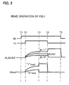
- Fig. 2 is a waveform diagram of a read operation for the semiconductor memory of Fig. 1.
- the word line WL is driven to H level to make the cell transistor conducting (time T1 in Fig. 2), after which the plate line PL is driven to H level (time T2).
- a positive voltage is applied to the ferroelectric capacitors F0, F1, FREF.
- the ferroelectric capacitor F0 of the normal memory cell MC0 which had been polarized in the positive direction (storing data "0"), has been applied a positive voltage with the same polarity as during writing, so that no polarization inversion occurs, only a slight amount of charge flows in the bit line BL0, and the potential of the bit line BL0 rises only slightly.
- the sense amplifiers SA0, SA1 When the sense amplifiers SA0, SA1 are activated (at time T3), the potentials of the normal bit lines BL0 and BL1 are detected with reference to the potential of the reference bit line BLREF and are amplified to ground potential (0 V) and to the power supply level (VDD level) respectively.
- the voltage detected by the sense amplifier is applied to the bit line while the plate line PL is lowered to L level (at time T4), so that in the case of memory cells to which data "1" had been written, because the bit line is at H level, a negative voltage is applied to the ferroelectric capacitor to perform re-writing.
- the polarization of a ferroelectric capacitor of a data "0" memory cell is not inverted, since the bit line is at L level and the plate line is at L level, and so the forward-direction polarization state is maintained.
- the word line WL is returned to L level (at time T5).
- the reference bit line BLREF is driven to ground level by a re-write circuit, not shown, and data "0" is written to the reference memory cell.
- Fig. 3 shows the configuration of the semiconductor memory in this embodiment.
- the configuration of the normal memory cells MCO and MC1, the word line WL, plate line PL, and normal bit lines BL0 and BL1 is the same as in Fig. 1.
- the reference memory cell MCREF has a cell transistor NREF and a reference ferroelectric capacitor FREF, and the capacitor FREF has the same area and the same structure as the ferroelectric capacitors F0 and F1 of the normal memory cells.
- a negative-direction polarization state (data "1") is always written to the reference memory cell MCREF through application of a negative voltage.
- an increase to a high potential occurs in the reference bit line BLREF, similarly to the bit line of a memory cell storing data "1".
- a current mirror circuit 10 in order to render read operations more stable, has a first transistor DSREF, the gate and drain of which are connected to the reference bit line BLREF, and a plurality of second transistors DS0, DS1 the drains of which are connected to the normal bit lines BL0, BL1, and the gates of which are connected to the reference bit line BLREF; the sources of these transistors are connected to a common power supply, such as for example a ground power supply.
- the first transistor DSREF and the second transistors DS0, DS1 are all connected to the same gate potential, so that the drain currents are proportional to the transistor size. That is, if the transistor size is the same, the drain currents are all equal.
- the normal memory cell MC0 stores data "0" (positive-direction polarization), and that MC1 stores data "1" (negative-direction polarization).
- data "1" (negative-direction polarization) is stored in the reference memory cell MCREF.
- the word line WL is driven to H level
- the cell transistors in the memory cells connected to the word line WL are made conducting.
- the plate line PL is then driven to H level, the amount of charge flowing out to the bit line BL0 from the memory cell MC0 storing data "0" (positive-direction polarization) is small, and there is little increase in the potential of the bit line BL0.
- bit lines BL1 and BLREF the amount of charge flowing into the bit lines BL1 and BLREF from the memory cells MC1 and MCREF, which store data "1" (negative-direction polarization), is large, so that there is a large increase in the potential of the bit lines BL1 and BLREF.
- the first transistor DSREF connected to the reference bit line BLREF is conducting, and causes the potential of the reference bit line BLREF to fall; this potential is higher than the ground potential, which is the source potential, by the amount of the threshold voltage of the first transistor DSREF.
- the reference bit line BLREF is also connected to the gates of the second transistors DS0 and DS1, so that due to conduction by the second transistor DS0 the potential of the normal bit line BL0 falls substantially to ground level, and due to conduction by the second transistor DS1 the potential of the normal bit line BL1 is at a level higher than ground potential, which is the source potential, by the amount of the threshold voltage of the second transistor DS1.
- the potential of normal bit lines held at a prescribed potential by the current mirror circuit 10 is amplified by the preamp circuits PA0 and PA1. That is, through control by the current mirror circuit 10, the potential of normal bit lines is held at either ground level or the threshold voltage level. In order to detect such a potential difference, use of a reference potential equal to one-half the threshold voltage is conceivable, but generating such a reference potential is not easy. Hence the preamp circuits PA0 and PA1 amplify the ground level and threshold voltage level of the normal bit line potentials, shifting the levels to a level lower than and higher than the threshold voltage level.
- the preamp circuits PA0, PA1 comprise p-channel precharge transistors PR0, PR1 the sources of which are connected to the power supply and to the gates of which is applied a precharge signal VPR, and amplification transistors CT0, CT1 the gates of which are connected to the reference bit line BLREF and the sources of which are respectively connected to the normal bit lines BL0, BL1.
- the precharge signal VPR goes to L level
- the precharge transistors PR0, PR1 are conducting, and the precharge nodes PN0, PN1 are precharged to the power supply level.
- the word line WL is driven to H level and the read operation starts, the reference bit line BLREF is held at threshold voltage level, the normal bit line BL0 is held at ground level, and the normal bit line BL1 is held at threshold voltage level (the same level as the reference bit line) by the above-described current mirror circuit 10. Then, the amplification transistor CT0 of the preamp PA0 is conducting, and the precharge node PN0 is lowered to ground level. On the other hand, the amplification transistor CT1 of the preamp PA1 is nonconducting, and the potential at the precharge node PN1 is lowered only somewhat. That is, the preamp amplification transistor compares the reference bit line potential and the normal bit line potential, and according to the comparison result executes control to either lower or not lower the precharge node level.
- the potentials at the precharge nodes PN0 and PN1 of the preamps PA0, PA1 are input to the sense amps SA0, SA1, comprising inverter circuits, and are amplified to the power supply level or ground level.
- These sense amp circuits may be ordinary CMOS inverter circuits not synchronized by a clock, or may be CMOS inverter circuits activated in synchronization with a clock signal.
- a preamp amplifies the potential of a normal bit line to a level either higher than or lower than the threshold voltage of the sense amp, and so the sense amp can easily detect the pre-amplified level.
- write circuits WA0, WA1 are provided, and the outputs SAout of the sense amps SA0, SA1 are fed back to the normal bit lines BL0, BL1 via the write circuits to perform re-writing.
- a write circuit switches to the re-write circuit at read time or to the write circuit at write time according to the write signal WE.
- the sense amp output SAout is inverted and transferred to the corresponding normal bit line.
- the plate line PL is then driven from H level to L level, so that re-writing of the ferroelectric capacitors of the normal memory cells is performed according to the feedback level on the normal bit lines BL0, BL1.
- Fig. 4 is a waveform diagram of a read operation for this embodiment. Operation is again explained referring to the waveform diagram.
- a precharge signal VPR at L level causes the precharge transistors PR0, PR1 to both be conducting, and the precharge nodes PN0, PN1 are precharged to the power supply level.
- the word line WL is driven to H level, and the cell transistors N0, N1, NREF of each of the memory cells are made conducting.
- a positive-direction voltage is applied to the ferroelectric capacitors F0, F1, FREF of all the memory cells.
- the amplification transistors CT0, CT1 of the preamps PA0, PA1 are both made conducting, and the potential at both precharge nodes PN0, PN1 falls.
- the normal bit line BL1 behaves similarly to the reference bit line BLREF, so that the amplification transistor CT1 of the preamp PA1 becomes nonconducting, and the decline in potential at the precharge node PN1 stops.
- the potential at the precharge node PN0 of the preamp PA0 falls to ground level.
- the potentials of the normal bit lines BL0 and BL1 are held at ground level and at the threshold voltage level Vth.
- the precharge node PN0 falls to near ground level, and the precharge node PN1 is held at close to power supply level.
- the output SAout of the sense amp SA0 rises to the power supply level, and the output SAout of the sense amp SA1 is maintained at ground level.
- a re-write circuit WAREF is provided on the side of the reference memory cell MCREF, and at time T5 the p-channel transistor thereof conducts in response to a L-level re-write signal /WE, and the reference bit line BLREF is driven to power supply level VDD. Then the plate line PL is driven to L level, so that a negative voltage is applied to the ferroelectric capacitor FREF of the reference memory cell to cause polarization in the negative direction, thus performing re-writing.
- On the reference bit line side there is no need to detect the level, and so there is no need to provide a preamp and sense amp; it is sufficient to provide a circuit which drives the reference bit line BLREF to H level with the re-write timing.
- the invention is applied to one-transistor, one-capacitor type ferroelectric memory.
- This type of memory has a simple memory cell circuit configuration, and so is appropriate for devices with large storage capacities.
- a current mirror circuit 10 in this embodiment, the potential of normal bit lines BL can always be driven to ground level or to the threshold voltage level Vth even when there is scattering in the capacitance values of ferroelectric capacitors, so that erroneous read operations can be suppressed.
- the current mirror circuit 10 in the above embodiment can also be applied to other types of semiconductor memory not using ferroelectric capacitors.
- capacitors using silicon oxide film and not using ferroelectric material there is little scattering in capacitance values even for processes currently in use, so that the advantages of the current mirror circuit 10 in preventing erroneous operation are not so great as in the case of application to ferroelectric capacitors.
Landscapes
- Engineering & Computer Science (AREA)
- Computer Hardware Design (AREA)
- Microelectronics & Electronic Packaging (AREA)
- Power Engineering (AREA)
- Dram (AREA)
- For Increasing The Reliability Of Semiconductor Memories (AREA)
Applications Claiming Priority (1)
| Application Number | Priority Date | Filing Date | Title |
|---|---|---|---|
| JP2005000555A JP4083173B2 (ja) | 2005-01-05 | 2005-01-05 | 半導体メモリ |
Publications (3)
| Publication Number | Publication Date |
|---|---|
| EP1688955A2 true EP1688955A2 (de) | 2006-08-09 |
| EP1688955A3 EP1688955A3 (de) | 2006-09-13 |
| EP1688955B1 EP1688955B1 (de) | 2008-07-30 |
Family
ID=36593190
Family Applications (1)
| Application Number | Title | Priority Date | Filing Date |
|---|---|---|---|
| EP05253805A Expired - Lifetime EP1688955B1 (de) | 2005-01-05 | 2005-06-20 | Halbleiterspeicher |
Country Status (5)
| Country | Link |
|---|---|
| US (1) | US7180766B2 (de) |
| EP (1) | EP1688955B1 (de) |
| JP (1) | JP4083173B2 (de) |
| KR (1) | KR100638233B1 (de) |
| DE (1) | DE602005008550D1 (de) |
Families Citing this family (12)
| Publication number | Priority date | Publication date | Assignee | Title |
|---|---|---|---|---|
| US7617134B2 (en) * | 2005-06-17 | 2009-11-10 | Match.Com, L.L.C. | System and method for providing a certified photograph in a network environment |
| US7933138B2 (en) * | 2009-01-30 | 2011-04-26 | Texas Instruments Incorporated | F-RAM device with current mirror sense amp |
| JP2013033566A (ja) * | 2011-08-01 | 2013-02-14 | Fujitsu Semiconductor Ltd | 半導体メモリおよびシステム |
| US9042187B2 (en) * | 2012-09-17 | 2015-05-26 | Intel Corporation | Using a reference bit line in a memory |
| US9281044B2 (en) * | 2013-05-17 | 2016-03-08 | Micron Technology, Inc. | Apparatuses having a ferroelectric field-effect transistor memory array and related method |
| US9786347B1 (en) * | 2016-03-16 | 2017-10-10 | Micron Technology, Inc. | Cell-specific reference generation and sensing |
| US9881661B2 (en) * | 2016-06-03 | 2018-01-30 | Micron Technology, Inc. | Charge mirror-based sensing for ferroelectric memory |
| US10074422B1 (en) | 2017-06-13 | 2018-09-11 | Cypress Semiconductor Corporation | 2T1C ferro-electric random access memory cell |
| JP7173594B2 (ja) * | 2017-12-08 | 2022-11-16 | 国立大学法人東北大学 | 抵抗変化型素子を備えた記憶回路及びセンスアンプ |
| US11705176B2 (en) | 2020-08-07 | 2023-07-18 | Tohoku University | Storage circuit provided with variable resistance type elements, and its test device |
| DE102020216060B4 (de) | 2020-12-16 | 2024-08-22 | Fraunhofer-Gesellschaft zur Förderung der angewandten Forschung eingetragener Verein | Elektrische Schaltungsanordnung mit einem ferroelektrischen Feldeffekttransistor und Speicherzelle |
| JP7677611B2 (ja) | 2021-03-03 | 2025-05-15 | 国立大学法人東北大学 | 抵抗変化型素子を備えた記憶回路 |
Citations (2)
| Publication number | Priority date | Publication date | Assignee | Title |
|---|---|---|---|---|
| JP2001118380A (ja) | 1999-09-08 | 2001-04-27 | Hyundai Electronics Ind Co Ltd | 不揮発性強誘電体メモリ装置 |
| JP2002100183A (ja) | 2000-09-26 | 2002-04-05 | Oki Electric Ind Co Ltd | 読み出し回路 |
Family Cites Families (4)
| Publication number | Priority date | Publication date | Assignee | Title |
|---|---|---|---|---|
| EP1304701A1 (de) | 2001-10-18 | 2003-04-23 | STMicroelectronics S.r.l. | Leseschaltung für nichtflüchtige ferroelektrische Speicher |
| JP3756873B2 (ja) * | 2002-11-11 | 2006-03-15 | 沖電気工業株式会社 | 半導体記憶装置 |
| JP2004288282A (ja) * | 2003-03-20 | 2004-10-14 | Fujitsu Ltd | 半導体装置 |
| JP4079910B2 (ja) | 2004-05-28 | 2008-04-23 | 富士通株式会社 | 強誘電体メモリ |
-
2005
- 2005-01-05 JP JP2005000555A patent/JP4083173B2/ja not_active Expired - Fee Related
- 2005-06-17 US US11/154,797 patent/US7180766B2/en not_active Expired - Lifetime
- 2005-06-20 EP EP05253805A patent/EP1688955B1/de not_active Expired - Lifetime
- 2005-06-20 DE DE602005008550T patent/DE602005008550D1/de not_active Expired - Lifetime
- 2005-07-05 KR KR1020050059978A patent/KR100638233B1/ko not_active Expired - Fee Related
Patent Citations (2)
| Publication number | Priority date | Publication date | Assignee | Title |
|---|---|---|---|---|
| JP2001118380A (ja) | 1999-09-08 | 2001-04-27 | Hyundai Electronics Ind Co Ltd | 不揮発性強誘電体メモリ装置 |
| JP2002100183A (ja) | 2000-09-26 | 2002-04-05 | Oki Electric Ind Co Ltd | 読み出し回路 |
Also Published As
| Publication number | Publication date |
|---|---|
| JP2006190377A (ja) | 2006-07-20 |
| DE602005008550D1 (de) | 2008-09-11 |
| KR100638233B1 (ko) | 2006-10-25 |
| EP1688955B1 (de) | 2008-07-30 |
| US7180766B2 (en) | 2007-02-20 |
| EP1688955A3 (de) | 2006-09-13 |
| JP4083173B2 (ja) | 2008-04-30 |
| KR20060080523A (ko) | 2006-07-10 |
| US20060146625A1 (en) | 2006-07-06 |
Similar Documents
| Publication | Publication Date | Title |
|---|---|---|
| EP1154436B1 (de) | Halbleiterspeicheranordnung | |
| JP3326560B2 (ja) | 半導体メモリ装置 | |
| US9299417B2 (en) | DRAM security erase | |
| US11790971B2 (en) | Ferroelectric random access memory device and method for operating read and write thereof | |
| JP3866913B2 (ja) | 半導体装置 | |
| CN102265396A (zh) | 电容隔离的失配补偿型读出放大器 | |
| EP1688955B1 (de) | Halbleiterspeicher | |
| US7280384B2 (en) | Semiconductor memory device | |
| KR100888834B1 (ko) | 강유전체 메모리 | |
| JP5190326B2 (ja) | 強誘電体メモリ装置 | |
| EP1030312B1 (de) | Ferroelektrischer Speicher | |
| KR100876900B1 (ko) | 센스 앰프와 그의 구동 방법 | |
| JP2007149296A (ja) | 不揮発性記憶装置およびその読出し方法 | |
| KR100369360B1 (ko) | 강유전체 메모리 장치 | |
| KR20240056489A (ko) | 통합식 다중 레벨형 메모리 장치 및 그 작동 방법 | |
| KR101171254B1 (ko) | 비트라인 센스앰프 제어 회로 및 이를 구비하는 반도체 메모리 장치 | |
| US7120045B2 (en) | Reference voltage generating apparatus for use in a ferroelectric random access memory (FRAM) and a driving method therefor | |
| KR100256253B1 (ko) | 비휘발성 반도체 메모리 장치 | |
| JP2004319047A (ja) | 強誘電体メモリ | |
| JP2000040377A (ja) | 不揮発性半導体記憶装置 | |
| JP2012003809A (ja) | 半導体記憶装置およびその駆動方法 | |
| KR20070073307A (ko) | 강유전체 메모리 장치 및 그것의 기입 방법 |
Legal Events
| Date | Code | Title | Description |
|---|---|---|---|
| PUAI | Public reference made under article 153(3) epc to a published international application that has entered the european phase |
Free format text: ORIGINAL CODE: 0009012 |
|
| AK | Designated contracting states |
Kind code of ref document: A2 Designated state(s): AT BE BG CH CY CZ DE DK EE ES FI FR GB GR HU IE IS IT LI LT LU MC NL PL PT RO SE SI SK TR |
|
| AX | Request for extension of the european patent |
Extension state: AL BA HR LV MK YU |
|
| PUAL | Search report despatched |
Free format text: ORIGINAL CODE: 0009013 |
|
| AK | Designated contracting states |
Kind code of ref document: A3 Designated state(s): AT BE BG CH CY CZ DE DK EE ES FI FR GB GR HU IE IS IT LI LT LU MC NL PL PT RO SE SI SK TR |
|
| AX | Request for extension of the european patent |
Extension state: AL BA HR LV MK YU |
|
| 17P | Request for examination filed |
Effective date: 20061009 |
|
| 17Q | First examination report despatched |
Effective date: 20061115 |
|
| AKX | Designation fees paid |
Designated state(s): DE FR GB |
|
| GRAP | Despatch of communication of intention to grant a patent |
Free format text: ORIGINAL CODE: EPIDOSNIGR1 |
|
| GRAS | Grant fee paid |
Free format text: ORIGINAL CODE: EPIDOSNIGR3 |
|
| GRAA | (expected) grant |
Free format text: ORIGINAL CODE: 0009210 |
|
| AK | Designated contracting states |
Kind code of ref document: B1 Designated state(s): DE FR GB |
|
| REG | Reference to a national code |
Ref country code: GB Ref legal event code: FG4D |
|
| REF | Corresponds to: |
Ref document number: 602005008550 Country of ref document: DE Date of ref document: 20080911 Kind code of ref document: P |
|
| REG | Reference to a national code |
Ref country code: GB Ref legal event code: 732E |
|
| REG | Reference to a national code |
Ref country code: FR Ref legal event code: TP |
|
| PLBE | No opposition filed within time limit |
Free format text: ORIGINAL CODE: 0009261 |
|
| STAA | Information on the status of an ep patent application or granted ep patent |
Free format text: STATUS: NO OPPOSITION FILED WITHIN TIME LIMIT |
|
| 26N | No opposition filed |
Effective date: 20090506 |
|
| PGFP | Annual fee paid to national office [announced via postgrant information from national office to epo] |
Ref country code: FR Payment date: 20090326 Year of fee payment: 5 |
|
| PGFP | Annual fee paid to national office [announced via postgrant information from national office to epo] |
Ref country code: GB Payment date: 20090625 Year of fee payment: 5 |
|
| GBPC | Gb: european patent ceased through non-payment of renewal fee |
Effective date: 20100620 |
|
| REG | Reference to a national code |
Ref country code: FR Ref legal event code: ST Effective date: 20110228 |
|
| PG25 | Lapsed in a contracting state [announced via postgrant information from national office to epo] |
Ref country code: FR Free format text: LAPSE BECAUSE OF NON-PAYMENT OF DUE FEES Effective date: 20100630 |
|
| PG25 | Lapsed in a contracting state [announced via postgrant information from national office to epo] |
Ref country code: GB Free format text: LAPSE BECAUSE OF NON-PAYMENT OF DUE FEES Effective date: 20100620 |
|
| REG | Reference to a national code |
Ref country code: DE Ref legal event code: R082 Ref document number: 602005008550 Country of ref document: DE Representative=s name: REICHERT & LINDNER PARTNERSCHAFT PATENTANWAELT, DE Ref country code: DE Ref legal event code: R081 Ref document number: 602005008550 Country of ref document: DE Owner name: FUJITSU SEMICONDUCTOR MEMORY SOLUTION LIMITED,, JP Free format text: FORMER OWNER: FUJITSU SEMICONDUCTOR LTD., YOKOHAMA, KANAGAWA, JP |
|
| PGFP | Annual fee paid to national office [announced via postgrant information from national office to epo] |
Ref country code: DE Payment date: 20200609 Year of fee payment: 16 |
|
| REG | Reference to a national code |
Ref country code: DE Ref legal event code: R119 Ref document number: 602005008550 Country of ref document: DE |
|
| PG25 | Lapsed in a contracting state [announced via postgrant information from national office to epo] |
Ref country code: DE Free format text: LAPSE BECAUSE OF NON-PAYMENT OF DUE FEES Effective date: 20220101 |