EP1669972A2 - Appareil d'affichage à plasma et son procédé de commande - Google Patents
Appareil d'affichage à plasma et son procédé de commande Download PDFInfo
- Publication number
- EP1669972A2 EP1669972A2 EP05257460A EP05257460A EP1669972A2 EP 1669972 A2 EP1669972 A2 EP 1669972A2 EP 05257460 A EP05257460 A EP 05257460A EP 05257460 A EP05257460 A EP 05257460A EP 1669972 A2 EP1669972 A2 EP 1669972A2
- Authority
- EP
- European Patent Office
- Prior art keywords
- waveform
- scan
- address
- electrode
- time point
- Prior art date
- Legal status (The legal status is an assumption and is not a legal conclusion. Google has not performed a legal analysis and makes no representation as to the accuracy of the status listed.)
- Ceased
Links
Images


Classifications
-
- G—PHYSICS
- G09—EDUCATION; CRYPTOGRAPHY; DISPLAY; ADVERTISING; SEALS
- G09G—ARRANGEMENTS OR CIRCUITS FOR CONTROL OF INDICATING DEVICES USING STATIC MEANS TO PRESENT VARIABLE INFORMATION
- G09G3/00—Control arrangements or circuits, of interest only in connection with visual indicators other than cathode-ray tubes
- G09G3/20—Control arrangements or circuits, of interest only in connection with visual indicators other than cathode-ray tubes for presentation of an assembly of a number of characters, e.g. a page, by composing the assembly by combination of individual elements arranged in a matrix no fixed position being assigned to or needed to be assigned to the individual characters or partial characters
- G09G3/22—Control arrangements or circuits, of interest only in connection with visual indicators other than cathode-ray tubes for presentation of an assembly of a number of characters, e.g. a page, by composing the assembly by combination of individual elements arranged in a matrix no fixed position being assigned to or needed to be assigned to the individual characters or partial characters using controlled light sources
- G09G3/28—Control arrangements or circuits, of interest only in connection with visual indicators other than cathode-ray tubes for presentation of an assembly of a number of characters, e.g. a page, by composing the assembly by combination of individual elements arranged in a matrix no fixed position being assigned to or needed to be assigned to the individual characters or partial characters using controlled light sources using luminous gas-discharge panels, e.g. plasma panels
- G09G3/288—Control arrangements or circuits, of interest only in connection with visual indicators other than cathode-ray tubes for presentation of an assembly of a number of characters, e.g. a page, by composing the assembly by combination of individual elements arranged in a matrix no fixed position being assigned to or needed to be assigned to the individual characters or partial characters using controlled light sources using luminous gas-discharge panels, e.g. plasma panels using AC panels
- G09G3/291—Control arrangements or circuits, of interest only in connection with visual indicators other than cathode-ray tubes for presentation of an assembly of a number of characters, e.g. a page, by composing the assembly by combination of individual elements arranged in a matrix no fixed position being assigned to or needed to be assigned to the individual characters or partial characters using controlled light sources using luminous gas-discharge panels, e.g. plasma panels using AC panels controlling the gas discharge to control a cell condition, e.g. by means of specific pulse shapes
- G09G3/293—Control arrangements or circuits, of interest only in connection with visual indicators other than cathode-ray tubes for presentation of an assembly of a number of characters, e.g. a page, by composing the assembly by combination of individual elements arranged in a matrix no fixed position being assigned to or needed to be assigned to the individual characters or partial characters using controlled light sources using luminous gas-discharge panels, e.g. plasma panels using AC panels controlling the gas discharge to control a cell condition, e.g. by means of specific pulse shapes for address discharge
-
- G—PHYSICS
- G09—EDUCATION; CRYPTOGRAPHY; DISPLAY; ADVERTISING; SEALS
- G09G—ARRANGEMENTS OR CIRCUITS FOR CONTROL OF INDICATING DEVICES USING STATIC MEANS TO PRESENT VARIABLE INFORMATION
- G09G3/00—Control arrangements or circuits, of interest only in connection with visual indicators other than cathode-ray tubes
- G09G3/20—Control arrangements or circuits, of interest only in connection with visual indicators other than cathode-ray tubes for presentation of an assembly of a number of characters, e.g. a page, by composing the assembly by combination of individual elements arranged in a matrix no fixed position being assigned to or needed to be assigned to the individual characters or partial characters
- G09G3/2007—Display of intermediate tones
- G09G3/2018—Display of intermediate tones by time modulation using two or more time intervals
- G09G3/2022—Display of intermediate tones by time modulation using two or more time intervals using sub-frames
-
- G—PHYSICS
- G09—EDUCATION; CRYPTOGRAPHY; DISPLAY; ADVERTISING; SEALS
- G09G—ARRANGEMENTS OR CIRCUITS FOR CONTROL OF INDICATING DEVICES USING STATIC MEANS TO PRESENT VARIABLE INFORMATION
- G09G3/00—Control arrangements or circuits, of interest only in connection with visual indicators other than cathode-ray tubes
- G09G3/20—Control arrangements or circuits, of interest only in connection with visual indicators other than cathode-ray tubes for presentation of an assembly of a number of characters, e.g. a page, by composing the assembly by combination of individual elements arranged in a matrix no fixed position being assigned to or needed to be assigned to the individual characters or partial characters
- G09G3/22—Control arrangements or circuits, of interest only in connection with visual indicators other than cathode-ray tubes for presentation of an assembly of a number of characters, e.g. a page, by composing the assembly by combination of individual elements arranged in a matrix no fixed position being assigned to or needed to be assigned to the individual characters or partial characters using controlled light sources
- G09G3/28—Control arrangements or circuits, of interest only in connection with visual indicators other than cathode-ray tubes for presentation of an assembly of a number of characters, e.g. a page, by composing the assembly by combination of individual elements arranged in a matrix no fixed position being assigned to or needed to be assigned to the individual characters or partial characters using controlled light sources using luminous gas-discharge panels, e.g. plasma panels
- G09G3/288—Control arrangements or circuits, of interest only in connection with visual indicators other than cathode-ray tubes for presentation of an assembly of a number of characters, e.g. a page, by composing the assembly by combination of individual elements arranged in a matrix no fixed position being assigned to or needed to be assigned to the individual characters or partial characters using controlled light sources using luminous gas-discharge panels, e.g. plasma panels using AC panels
- G09G3/291—Control arrangements or circuits, of interest only in connection with visual indicators other than cathode-ray tubes for presentation of an assembly of a number of characters, e.g. a page, by composing the assembly by combination of individual elements arranged in a matrix no fixed position being assigned to or needed to be assigned to the individual characters or partial characters using controlled light sources using luminous gas-discharge panels, e.g. plasma panels using AC panels controlling the gas discharge to control a cell condition, e.g. by means of specific pulse shapes
- G09G3/292—Control arrangements or circuits, of interest only in connection with visual indicators other than cathode-ray tubes for presentation of an assembly of a number of characters, e.g. a page, by composing the assembly by combination of individual elements arranged in a matrix no fixed position being assigned to or needed to be assigned to the individual characters or partial characters using controlled light sources using luminous gas-discharge panels, e.g. plasma panels using AC panels controlling the gas discharge to control a cell condition, e.g. by means of specific pulse shapes for reset discharge, priming discharge or erase discharge occurring in a phase other than addressing
- G09G3/2927—Details of initialising
-
- G—PHYSICS
- G09—EDUCATION; CRYPTOGRAPHY; DISPLAY; ADVERTISING; SEALS
- G09G—ARRANGEMENTS OR CIRCUITS FOR CONTROL OF INDICATING DEVICES USING STATIC MEANS TO PRESENT VARIABLE INFORMATION
- G09G3/00—Control arrangements or circuits, of interest only in connection with visual indicators other than cathode-ray tubes
- G09G3/20—Control arrangements or circuits, of interest only in connection with visual indicators other than cathode-ray tubes for presentation of an assembly of a number of characters, e.g. a page, by composing the assembly by combination of individual elements arranged in a matrix no fixed position being assigned to or needed to be assigned to the individual characters or partial characters
- G09G3/22—Control arrangements or circuits, of interest only in connection with visual indicators other than cathode-ray tubes for presentation of an assembly of a number of characters, e.g. a page, by composing the assembly by combination of individual elements arranged in a matrix no fixed position being assigned to or needed to be assigned to the individual characters or partial characters using controlled light sources
- G09G3/28—Control arrangements or circuits, of interest only in connection with visual indicators other than cathode-ray tubes for presentation of an assembly of a number of characters, e.g. a page, by composing the assembly by combination of individual elements arranged in a matrix no fixed position being assigned to or needed to be assigned to the individual characters or partial characters using controlled light sources using luminous gas-discharge panels, e.g. plasma panels
- G09G3/288—Control arrangements or circuits, of interest only in connection with visual indicators other than cathode-ray tubes for presentation of an assembly of a number of characters, e.g. a page, by composing the assembly by combination of individual elements arranged in a matrix no fixed position being assigned to or needed to be assigned to the individual characters or partial characters using controlled light sources using luminous gas-discharge panels, e.g. plasma panels using AC panels
- G09G3/291—Control arrangements or circuits, of interest only in connection with visual indicators other than cathode-ray tubes for presentation of an assembly of a number of characters, e.g. a page, by composing the assembly by combination of individual elements arranged in a matrix no fixed position being assigned to or needed to be assigned to the individual characters or partial characters using controlled light sources using luminous gas-discharge panels, e.g. plasma panels using AC panels controlling the gas discharge to control a cell condition, e.g. by means of specific pulse shapes
- G09G3/294—Control arrangements or circuits, of interest only in connection with visual indicators other than cathode-ray tubes for presentation of an assembly of a number of characters, e.g. a page, by composing the assembly by combination of individual elements arranged in a matrix no fixed position being assigned to or needed to be assigned to the individual characters or partial characters using controlled light sources using luminous gas-discharge panels, e.g. plasma panels using AC panels controlling the gas discharge to control a cell condition, e.g. by means of specific pulse shapes for lighting or sustain discharge
- G09G3/2948—Control arrangements or circuits, of interest only in connection with visual indicators other than cathode-ray tubes for presentation of an assembly of a number of characters, e.g. a page, by composing the assembly by combination of individual elements arranged in a matrix no fixed position being assigned to or needed to be assigned to the individual characters or partial characters using controlled light sources using luminous gas-discharge panels, e.g. plasma panels using AC panels controlling the gas discharge to control a cell condition, e.g. by means of specific pulse shapes for lighting or sustain discharge by increasing the total sustaining time with respect to other times in the frame
-
- G—PHYSICS
- G09—EDUCATION; CRYPTOGRAPHY; DISPLAY; ADVERTISING; SEALS
- G09G—ARRANGEMENTS OR CIRCUITS FOR CONTROL OF INDICATING DEVICES USING STATIC MEANS TO PRESENT VARIABLE INFORMATION
- G09G3/00—Control arrangements or circuits, of interest only in connection with visual indicators other than cathode-ray tubes
- G09G3/20—Control arrangements or circuits, of interest only in connection with visual indicators other than cathode-ray tubes for presentation of an assembly of a number of characters, e.g. a page, by composing the assembly by combination of individual elements arranged in a matrix no fixed position being assigned to or needed to be assigned to the individual characters or partial characters
- G09G3/22—Control arrangements or circuits, of interest only in connection with visual indicators other than cathode-ray tubes for presentation of an assembly of a number of characters, e.g. a page, by composing the assembly by combination of individual elements arranged in a matrix no fixed position being assigned to or needed to be assigned to the individual characters or partial characters using controlled light sources
- G09G3/28—Control arrangements or circuits, of interest only in connection with visual indicators other than cathode-ray tubes for presentation of an assembly of a number of characters, e.g. a page, by composing the assembly by combination of individual elements arranged in a matrix no fixed position being assigned to or needed to be assigned to the individual characters or partial characters using controlled light sources using luminous gas-discharge panels, e.g. plasma panels
- G09G3/288—Control arrangements or circuits, of interest only in connection with visual indicators other than cathode-ray tubes for presentation of an assembly of a number of characters, e.g. a page, by composing the assembly by combination of individual elements arranged in a matrix no fixed position being assigned to or needed to be assigned to the individual characters or partial characters using controlled light sources using luminous gas-discharge panels, e.g. plasma panels using AC panels
- G09G3/296—Driving circuits for producing the waveforms applied to the driving electrodes
-
- G—PHYSICS
- G09—EDUCATION; CRYPTOGRAPHY; DISPLAY; ADVERTISING; SEALS
- G09G—ARRANGEMENTS OR CIRCUITS FOR CONTROL OF INDICATING DEVICES USING STATIC MEANS TO PRESENT VARIABLE INFORMATION
- G09G2310/00—Command of the display device
- G09G2310/02—Addressing, scanning or driving the display screen or processing steps related thereto
- G09G2310/0202—Addressing of scan or signal lines
- G09G2310/0218—Addressing of scan or signal lines with collection of electrodes in groups for n-dimensional addressing
-
- G—PHYSICS
- G09—EDUCATION; CRYPTOGRAPHY; DISPLAY; ADVERTISING; SEALS
- G09G—ARRANGEMENTS OR CIRCUITS FOR CONTROL OF INDICATING DEVICES USING STATIC MEANS TO PRESENT VARIABLE INFORMATION
- G09G2320/00—Control of display operating conditions
- G09G2320/02—Improving the quality of display appearance
- G09G2320/0228—Increasing the driving margin in plasma displays
-
- G—PHYSICS
- G09—EDUCATION; CRYPTOGRAPHY; DISPLAY; ADVERTISING; SEALS
- G09G—ARRANGEMENTS OR CIRCUITS FOR CONTROL OF INDICATING DEVICES USING STATIC MEANS TO PRESENT VARIABLE INFORMATION
- G09G2320/00—Control of display operating conditions
- G09G2320/04—Maintaining the quality of display appearance
- G09G2320/041—Temperature compensation
-
- G—PHYSICS
- G09—EDUCATION; CRYPTOGRAPHY; DISPLAY; ADVERTISING; SEALS
- G09G—ARRANGEMENTS OR CIRCUITS FOR CONTROL OF INDICATING DEVICES USING STATIC MEANS TO PRESENT VARIABLE INFORMATION
- G09G2330/00—Aspects of power supply; Aspects of display protection and defect management
- G09G2330/02—Details of power systems and of start or stop of display operation
- G09G2330/025—Reduction of instantaneous peaks of current
-
- G—PHYSICS
- G09—EDUCATION; CRYPTOGRAPHY; DISPLAY; ADVERTISING; SEALS
- G09G—ARRANGEMENTS OR CIRCUITS FOR CONTROL OF INDICATING DEVICES USING STATIC MEANS TO PRESENT VARIABLE INFORMATION
- G09G2330/00—Aspects of power supply; Aspects of display protection and defect management
- G09G2330/06—Handling electromagnetic interferences [EMI], covering emitted as well as received electromagnetic radiation
Definitions
- the present invention relates to a plasma display apparatus and a driving method thereof.
- a plasma display apparatus comprises a plasma display panel where one unit cell is provided at a space between barrier ribs formed between a front substrate and a rear substrate.
- a main discharge gas such as neon (Ne), helium (He) or a mixture (He+Ne) of neon and helium and inert gas containing a small amount of xenon (Xe) are filled in each cell.
- the inert gas When discharge is performed using high frequency voltage, the inert gas generates vacuum ultraviolet rays, and causing phosphors provided between the barrier ribs to emit visible light, thereby realizing an image.
- the plasma display panel is attracting attention as a next generation display due to its slimness and light weight.
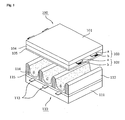
- FIG. 1 illustrates a structure of a conventional plasma display panel.
- a plasma display panel comprises a front substrate 100 and a rear substrate 110.
- the front substrate 100 has a plurality of sustain electrode pairs arranged with a scan electrode 102 and a sustain electrode 103 each paired and formed on a front glass 101, which is a display surface for displaying the image thereon.
- the rear substrate 110 has a plurality of address electrodes 113 arranged to intersect with the plurality of sustain electrode pairs on a front glass 111, which is spaced apart in parallel with and attached to the front substrate 100.
- the front substrate 100 includes the paired scan electrode 102 and the paired sustain electrode 103 for performing a mutual discharge in one pixel and sustaining emission of light, that is, the paired scan electrode 102 and the paired sustain electrode 103 each having a transparent electrode (a) formed of indium-tin-oxide (ITO) and a bus electrode (b) formed of metal.
- the scan electrode 102 and the sustain electrode 103 are covered with at least one dielectric layer 104, which controls a discharge current and insulates the paired electrodes.
- a protective layer 105 is formed of magnesium oxide (MgO) on the dielectric layer 104 to facilitate a discharge condition.
- MgO magnesium oxide
- the rear substrate 110 includes stripe-type (or well-type) barrier ribs 112 for forming a plurality of discharge spaces (that is, discharge cells) and arranged in parallel. Also, the rear substrate 110 comprises a plurality of address electrodes 113 arranged in parallel with the barrier ribs 112, and performing an address discharge and generating the vacuum ultraviolet rays. Red (R), green (G), blue (B) phosphors 114 emit visible rays for displaying the image in the address discharge, and are coated over an upper surface of the rear substrate 110. Lower dielectric layer 115 for protecting the address electrode 113 is formed between the address electrode 113 and the phosphor 114.
- the discharge cells are formed in matrix in plural, and a driving module having a driving circuit for supplying a predetermined pulse to the discharge cell is connected and driven.
- FIG. 2 is a view illustrating a conventional method for expressing the image gray level in a plasma display apparatus.
- each subfield is divided into a reset period (RPD) for initializing all cells, an address period (APD) for selecting a discharged cell, and a sustain period (SPD) for expressing the gray level depending on the durations of discharge.
- RPD reset period
- APD address period
- SPD sustain period
- the reset period and the address period are the same for each subfield.
- the address discharge for selecting the cell to be discharged is generated by a voltage difference between the address electrode and the scan electrode being the transparent electrode.
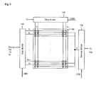
- FIG. 3 illustrates a charge state within a conventional discharge cell.
- the space charges 701 being charges existing in a space within the discharge cell, refer to charges not participating in the discharge unlike the wall charges 700.
- the recombination ratio between the space charges 701 and the wall charges 700 increases in the address period to decrease an amount of the wall charges 700 participating in the address discharge, thereby destabilizing the address discharge.
- the later the addressing is in sequence the more the time taken to recombine the space charges 701 with the wall charges 700 is sufficiently secured, thereby more destabilizing the address discharge. Therefore, there occurs the high-temperature erroneous discharge where the discharge cell turned-on in the address period is turned off in the sustain period.
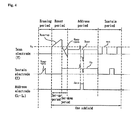
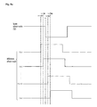
- FIG. 4 illustrates a driving waveform of a conventional plasma display apparatus.
- the conventional plasma display apparatus is driven with each subfield divided into the reset period for initializing all cells, the address period for selecting the cell to be discharged, the sustain period for sustaining a discharge of the selected cell, and the erasure period for erasing the wall charge within the discharge cell.
- all address waveforms applied to the address electrodes (X 1 to Xn) are applied at the same time "ts" as the scan waveform applied to the scan electrode in the address period. If the address waveform and the scan waveform are applied to the address electrodes (X 1 to Xn) and the scan electrode respectively at the same time point, a noise is generated at the waveform applied to the scan electrode and the waveform applied to the sustain electrode.
- This noise results from coupling through capacitance of the panel.
- an up noise is generated at the waveform applied to the scan electrode and the sustain electrode
- a down noise is generated at the waveform applied to the scan electrode and the sustain electrode.
- the present invention is made with the problems and disadvantages of the background art in mind.
- a plasma display apparatus comprising: a plasma display panel comprising a plurality of scan electrodes, sustain electrodes, and address electrodes intersecting with the scan electrodes; a scan driver for applying a negative waveform and a reset waveform subsequent to the negative waveform to the scan electrode, and applying a scan waveform subsequent to the reset waveform to the scan electrode; a sustain driver for applying a positive waveform corresponding to the negative waveform to the sustain electrode; and a data driver for applying an address waveform to the address electrode, wherein a scan waveform is applied to one scan electrode and applying time points among at least two address waveforms applied to the address electrode corresponding to the scan waveform are different from each other, wherein, when the temperature of the plasma display panel is more than a threshold temperature, an idle period from an applying time point of a last sustain waveform applied to the scan electrode or the sustain electrode to an applying time point of a predetermined waveform gets different.
- a plasma display apparatus comprising: a plasma display panel comprising a plurality of scan electrodes, sustain electrodes, and address electrodes intersecting with the scan electrodes; a scan driver for applying a negative waveform and a reset waveform subsequent to the negative waveform to the scan electrode, and applying a scan waveform subsequent to the reset waveform to the scan electrode; and a sustain driver for applying a positive waveform corresponding to the negative waveform to the sustain electrode, wherein, when the temperature of the plasma display panel is more than a threshold temperature, an idle period from an applying time point of a last sustain waveform applied to the scan electrode or the sustain electrode to an applying time point of a predetermined waveform gets different.
- a driving method of a plasma display apparatus having a plasma display panel comprising a plurality of scan electrodes, sustain electrodes, and address electrodes intersecting with the scan electrodes, the method comprising the steps of: applying a negative waveform to the scan electrode, and applying a positive waveform corresponding to the negative waveform, to the sustain electrode; and applying a reset waveform subsequent to the negative waveform to the scan electrode, applying a scan waveform subsequent to the reset waveform, applying an address waveform to the address electrode, wherein a scan waveform is applied to one scan electrode and applying time points among at least two address waveforms applied to the address electrode corresponding to the scan waveform are different from each other, wherein, when the temperature of the plasma display panel is more than a threshold temperature, an idle period from an applying time point of a last sustain waveform applied to the scan electrode or the sustain electrode to an applying time point of a predetermined waveform gets different.
- embodiments may provide an improved plasma display apparatus and driving method thereof by suppressing a high temperature erroneous discharge of the plasma display panel.
- embodiments may provide an improved plasma display apparatus and driving method thereof by reducing noise generated in an address period, and improving a driving margin.
- embodiments may provide an improved plasma display apparatus and driving method thereof by sufficiently securing a driving period of a plasma display apparatus, and more stably driving the plasma display apparatus.
- a plasma display apparatus comprising: a plasma display panel comprising a plurality of scan electrodes, sustain electrodes, and address electrodes intersecting with the scan electrodes; a scan driver for applying a negative waveform and a reset waveform subsequent to the negative waveform to the scan electrode, and applying a scan waveform subsequent to the reset waveform to the scan electrode; a sustain driver for applying a positive waveform corresponding to the negative waveform to the sustain electrode; and a data driver for applying an address waveform to the address electrode, wherein a scan waveform is applied to one scan electrode and applying time points among at least two address waveforms applied to the address electrode corresponding to the scan waveform are different from each other, wherein, when the temperature of the plasma display panel is more than a threshold temperature, an idle period from an applying time point of a last sustain waveform applied to the scan electrode or the sustain electrode to an applying time point of a predetermined waveform gets different.
- the predetermined waveform may be any one of a setup waveform, a setdown waveform, or a scan waveform.
- the scan driver may set a first threshold temperature and, when the temperature of the plasma display panel is more than the first threshold temperature, makes the idle period longer than when it is less than the first threshold temperature.
- the first threshold temperature may be 40 °C.
- the idle period may be 100 ⁇ s to 1 ms.
- the last sustain waveform may have a pulsewidth of 1 ⁇ s to 1 ms.
- the address waveforms corresponding to the same scan waveforms and applied to the mutually different address electrodes may have mutually different applying time points.
- the negative waveform is a ramp-down waveform, and the positive waveform may be constantly sustained.
- a plasma display apparatus comprising: a plasma display panel comprising a plurality of scan electrodes, sustain electrodes, and address electrodes intersecting with the scan electrodes; a scan driver for applying a negative waveform and a reset waveform subsequent to the negative waveform to the scan electrode, and applying a scan waveform subsequent to the reset waveform to the scan electrode; and a sustain driver for applying a positive waveform corresponding to the negative waveform to the sustain electrode, wherein, when the temperature of the plasma display panel is more than a threshold temperature, an idle period from an applying time point of a last sustain waveform applied to the scan electrode or the sustain electrode to an applying time point of a predetermined waveform gets different.
- the scan driver may set a first threshold temperature and, when the temperature of the plasma display panel is more than the first threshold temperature, makes the idle period longer than when it is less than the first threshold temperature.
- the first threshold temperature may be 40 °C.
- the idle period may be 100 ⁇ s to 1 ms.
- the last sustain waveform may have a pulsewidth of 1 ⁇ s to 1 ms.
- the negative waveform may be a ramp-down waveform, and the positive waveform may be constantly sustained.
- a driving method of a plasma display apparatus having a plasma display panel comprising a plurality of scan electrodes, sustain electrodes, and address electrodes intersecting with the scan electrodes, the method comprising the steps of: applying a negative waveform to the scan electrode, and applying a positive waveform corresponding to the negative waveform, to the sustain electrode; and applying a reset waveform subsequent to the negative waveform to the scan electrode, applying a scan waveform subsequent to the reset waveform, applying an address waveform to the address electrode, wherein a scan waveform is applied to one scan electrode and applying time points among at least two address waveforms applied to the address electrode corresponding to the scan waveform are different from each other, corresponding to the scan waveforms, wherein, when the temperature of the plasma display panel is more than a threshold temperature, an idle period from an applying time point of a last sustain waveform applied to the scan electrode or the sustain electrode to an applying time point of a predetermined waveform gets different.
- the idle period may be 100 ⁇ s to 1 ms.
- the last sustain waveform may have a pulsewidth of 1 ⁇ s to 1 ms.
- FIG. 1 illustrates a structure of a conventional plasma display panel
- FIG. 2 illustrates a conventional method for expressing a gray level of an image in a plasma display apparatus
- FIG. 3 illustrates a charge state within a conventional discharge cell
- FIG. 4 illustrates a driving waveform of a conventional plasma display apparatus
- FIG. 5 illustrates a plasma display apparatus according to a first embodiment of the present invention
- FIG. 6 illustrates a driving waveform according to the first embodiment of the present invention
- FIG. 7 illustrates other driving waveforms according to the first embodiment of the present invention.
- FIGS. 8A to 8E illustrate driving waveforms of an address period according to the first embodiment of the present invention
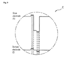
- FIG. 9 illustrates a region 'C' of FIG. 6
- FIGS. 10A to 10C illustrate other driving waveforms of an address period according to the first embodiment of the present invention
- FIG. 11 illustrates another driving waveform of an address period according to the first embodiment of the present invention
- FIGS. 12A to 12C illustrates a driving waveform of FIG. 11 in more detail
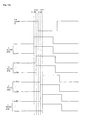
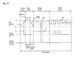
- FIG. 13 illustrates a driving waveform according to a second embodiment of the present invention
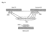
- FIG. 14 illustrates a charge state within a discharge cell according to the second embodiment of the present invention.
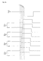
- FIG. 15 illustrates a driving waveform according to a third embodiment of the present invention.
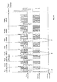
- a plasma display apparatus comprises a plasma display panel 500, a data driver 510, a scan driver 520, and a sustain driver 530.
- the plasma display panel 500 is formed by sealing front substrate (not shown) and a rear substrate (not shown).
- the front substrate has scan electrodes (Y1 to Yn) and a sustain electrode (Z), and the rear substrate has a plurality of address electrodes (X1 to Xm) intersecting with the scan electrodes (Y 1 to Yn) and the sustain electrode (Z).
- the data driver 510 applies data to the address electrodes (X1 to Xm) of the plasma display panel 500.
- the data refers to image signal data processed in an image signal processor (not shown) for processing an image signal received from the external.
- the data driver 510 samples and latches the data in response to a data timing control signal (CTRX) from a timing controller (not shown), and then applies an address waveform having an address voltage (Va) to each of the address electrodes (X1 to Xm).
- CTRX data timing control signal
- Va address voltage
- at least two address waveforms having different applying time points corresponding to the scan waveforms are applied to the address electrodes.
- the applying time point of the address waveform applied to the address electrode can be controlled, thereby reducing noise generated in the address period. This will be in detail described later with reference to FIGS. 8A to 12A.
- the scan driver 520 drives the scan electrodes (Y1 to Yn) of the plasma display panel 500.
- the scan driver 520 applies a setup waveform having a ramp-up formed by a combination of a sustain voltage (Vs) and a setup voltage (Vsetup), during a setup period of the reset period in response to a scan timing control signal (CTRY) from the timing controller (not shown).
- CTRY scan timing control signal
- the scan driver 520 applies a ramp-down setdown waveform consequently to the setup waveform, to the scan electrodes (Y1 to Yn) during a setdown period of the reset period.
- the scan driver 520 sequentially applies a scan waveform with a scan voltage (-Vy) to a scan reference voltage (Vsc), to each of the scan electrodes (Y1 to Yn) during an address period.
- the scan driver 520 applies at least one sustain waveform with a ground level (GND) to the sustain voltage (Vs) for a display discharge, to the scan electrodes (Y1 to Yn) during the sustain period.
- GDD ground level
- the sustain driver 530 drives the sustain electrode (Z) formed as a common electrode in the plasma display panel 500.
- the sustain driver 530 applies a waveform having a positive bias voltage (Vzb), to the sustain electrode (Z) during the address period in response to a scan timing control signal (CTRZ) from the timing controller (not shown).
- CTRZ scan timing control signal
- the sustain driver 530 applies at least one sustain waveform with the ground level (GND) to the sustain voltage (Vs), to the sustain electrode (Z) during the sustain period.
- an idle period from an applying time point of the sustain waveform applied to the scan electrodes (Y1 to Yn) or the sustain electrode (Z) to an applying time point of a predetermined waveform changes depending on the temperature of the plasma display panel 500.
- the predetermined waveform being any one of the setup waveform, the setdown waveform, and the scan waveform, is a waveform initially applied at a next frame after a last sustain waveform is applied.
- the idle period is defined as a period from an applying time point of a last sustain waveform of a current frame to a time point where a next frame is initiated.
- the idle period can be controlled depending on the temperature of the plasma display panel 500, thereby suppressing a high temperature erroneous discharge. This will be in detail described with reference to FIGS. 6 and 7 below.
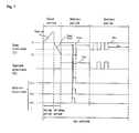
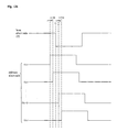
- FIG. 6 illustrates a driving waveform according to the first embodiment of the present invention.
- a plasma display apparatus is driven with each subfield divided into the reset period for initializing all cells, the address period for selecting a cell to be discharged, and the sustain period for sustaining a discharge of the selected cell.
- the ramp-up setup waveform is concurrently applied to all scan electrodes.
- a weak dark discharge is generated within discharge cells of the whole screen.
- positive wall charges become accumulated on the address electrode and the sustain electrode, and negative wall charges become accumulated on the scan electrode.
- the setdown waveform falling from the ground level (GND) to a predetermined voltage (-Vy) level is applied to all scan electrodes. Accordingly, an erasure discharge is generated between the scan electrode and the address electrode within the cells, thereby sufficiently erasing the wall charges formed between the scan electrode and the address electrode.
- the setdown waveform wall charges of such an amount that an address discharge can be stably generated within the cells where an image is to be displayed in the sustain period uniformly remain within the cells.
- a second falling waveform performs a function similar with a conventional setdown waveform.
- a negative scan waveform is sequentially applied to the scan electrodes and at the same time, is synchronized to the scan waveform so that a positive address waveform is applied to the address electrode.
- the respective potential differences between the scan waveform and the address waveform and a wall voltage generated in the reset period are added, thereby generating the address discharge within the discharge cell to which the address waveform is applied.
- the wall charges are formed in such an amount that a discharge can be generated when the sustain waveform of the sustain voltage (Vs) level is applied.
- a waveform having the positive bias voltage (Vzb) is applied to the sustain electrode to reduce a potential difference with the scan electrode during the address period, thereby not generating erroneous discharge with the scan electrode.
- at least two address waveforms having different applying time points corresponding to the scan waveform are applied in the address period of one subfield.
- the positive sustain waveform (Sus) is alternately applied to the scan electrode and the sustain electrodes.
- the cell selected by the address discharge generates the sustain discharge between the scan electrode and the sustain electrode, that is, the display discharge whenever the sustain waveform is applied.
- the idle period in the address period of one subfield, at least two address waveforms having different applying time points corresponding to the scan waveform are applied and together with this, the idle period changes depending on the temperature of the plasma display panel.
- the idle period is a period (WS1) for sustaining the ground level (GND) after the last one (SUSL) of the sustain waveforms applied in the sustain period falls from the sustain voltage (Vs) to the ground level (GND).
- the idle period is 100 ⁇ s to 1 ms.
- the space charges within the discharge cell that mainly cause the high temperature erroneous discharge within a range of 100 ⁇ s to 1 ms can be effectively reduced.
- a period from a time point of generating the last sustain discharge to a time point of initiating a next subfield is set to be sufficiently long, thereby securing enough time to reduce the space charges after the last sustain discharge.
- a reason for setting a lower limit threshold value to 100 ⁇ s is to sufficiently reduce the space charges generated in the sustain discharge of the plasma display apparatus, and a reason of setting an upper limit threshold value to 1 ms is to secure an operation margin of the sustain period of the plasma display apparatus.
- time limits may be employed with other embodiments of the invention as appropriate, according to the properties of the apparatus to which the invention is applied.
- the idle period gets longer as the plasma display panel increases in temperature. This is because as the temperature of the plasma display panel increases, the space charges of the discharge cell increase.
- the scan driver sets a first threshold temperature, and controls the idle period when the temperature of the plasma display panel exceeds the first threshold temperature to be longer than the idle period when it is less than the first threshold temperature.
- the first threshold temperature is set at 40 °C.
- high temperature is a factor having influence on the driving of the plasma display apparatus, that is, the first threshold temperature is set to 40 °C, but when the plasma display apparatus is variously changed in structure, the first threshold temperature will need to be set according to the requirements of the particular display.
- a plurality of threshold values such as second and third threshold temperatures together with the first threshold temperature can be also set to stepwise change the idle period depending on the temperature of the plasma display panel.
- the subfield where the idle period is controlled can be arbitrarily selected within one frame.
- at least one subfield is selected to control the idle period in order to more effectively reduce the high temperature erroneous discharge and secure a margin of a driving period. For example, it is possible to detect a subfield where space charges are generated in greater amounts as the temperature increases, and concentrate the increase the idle period of the subfield accordingly.
- the driving waveform is sustained to be at the ground level (GND) in the idle period, thereby reducing the space charges, but it is possible to differently apply the driving waveform as in FIG. 7 below.
- other driving waveforms of the plasma display apparatus are also divided on the basis of the reset period for initializing all cells, the address period for selecting the cell to be discharged, and the sustain period for sustaining the discharge of the selected cell.
- the address period at least two address waveforms having different applying time points corresponding to the scan waveform in the address period of one subfield are applied. A description of each period has been sufficiently made with reference to in FIG. 6 and accordingly, will be omitted.
- the high temperature erroneous discharge is suppressed by controlling a supply period of the sustain waveform for generating the last sustain discharge in the idle period.
- a period where the last sustain waveform sustains the sustain voltage (Vs) is an idle period (Ws2).
- the idle period is controlled within a range of 1 ⁇ s to 1 ms.
- the reason for setting the lower limit threshold value to 1 ⁇ s is to generate a sustain discharge of a desired magnitude, and a reason of setting the upper limit threshold value to 1 ms is to sufficiently reduce the space charges generated in the sustain discharge and, concurrently, secure the operation margin of the sustain period of the plasma display apparatus.
- a method for applying the at least two address waveforms having the different applying time points corresponding to the scan waveform can be variously modified. First, a method for applying the address waveform at a different applying time point from the scan waveform to each of a plurality of address electrodes will be described with reference to FIGS. 8A to 8E.
- the driving waveform of the address period in the driving waveform of the address period according to the first embodiment, at least two address waveforms are applied earlier or later than the scan waveform.
- the address waveform is applied to the address electrode (X1) at a time point earlier by 2 ⁇ t than a time point at which the scan waveform is applied to the scan electrode (Y), that is, at a time point "ts-2 ⁇ t” adaptively to an arrangement sequence of the address electrodes (X1 to Xn).
- the address waveform is applied to the address electrode (X2) at a time point earlier by ⁇ t than a time point at which the scan waveform is applied to the scan electrode (Y), that is, at a time point "ts- ⁇ t".
- the address waveform is applied to the electrode (Xn-1) at a time point "ts+ ⁇ t”
- the address waveform is applied to the electrode (Xn) at a time point "ts+2 ⁇ t”.
- the address waveform is applied to the address electrodes (X1 to Xn) before or after the applying time point of the scan waveform applied to the scan electrode (Y).
- the applying time points of the address waveforms applied to the address electrodes (X1 to Xn) are later than the applying time point of the scan waveform applied to the scan electrode (Y).
- the applying time point of the scan waveform applied to the scan electrode (Y) is "ts”
- the address waveform is applied to the address electrode (X1) at a time point later by ⁇ t than a time point at which the scan waveform is applied to the scan electrode (Y), that is, at a time point "ts+ ⁇ t” adaptively to an arrangement sequence of the address electrodes (X1 to Xn).
- the address waveform is applied to the address electrode (X2) at a time point later by 2 ⁇ t than a time point at which the scan waveform is applied to the scan electrode (Y), that is, at a time point "ts+2 ⁇ t".
- the address waveform is applied to the address electrode (X3) at a time point "ts+3 ⁇ t”
- the address waveform is applied to the electrode (Xn) at a time point "ts+n ⁇ t".
- a voltage difference between the scan electrode (Y) and the address electrode (X1) becomes 100V by the scan waveform applied to the scan electrode (Y), and, after a time " ⁇ t" has elapsed after the applying of the scan waveform, a voltage difference between the scan electrode (Y) and the address electrode (X1) rises to 170V by the address waveform applied to the address electrode (X1).
- the voltage difference between the scan electrode (Y) and the address electrode (X1) becomes an address discharge firing voltage, thereby generating the address discharge between the scan electrode (Y) and the address electrodes (X1 to Xn).
- the address waveform can be sequentially applied to a next address electrode, thereby reducing noise generated in the waveform applied to the scan electrode or the sustain electrode. Together with this, as the address discharge is sequentially generated, a more stable driving can be performed.
- the applying time points of the address waveforms applied to the address electrodes (X1 to Xn) are earlier than the applying time point of the scan waveform applied to the scan electrode (Y).
- the applying time point of the scan waveform applied to the scan electrode (Y) is "ts”
- the address waveform is applied to the address electrode (X1) at a time point later by ⁇ t than a time point at which the scan waveform is applied to the scan electrode (Y), that is, at a time point "ts- ⁇ t” adaptively to an arrangement sequence of the address electrodes (X1 to Xn).
- the address waveform is applied to the address electrode (X2) at a time point earlier by 2 ⁇ t than a time point at which the scan waveform is applied to the scan electrode (Y), that is, at a time point "ts-2 ⁇ t".
- the address waveform is applied to the address electrode (X3) at a time point "ts-3 ⁇ t”
- the address waveform is applied to the electrode (Xn) at a time point "ts-n ⁇ t".
- a voltage difference between the scan electrode (Y) and the address electrode (X1) becomes 100V by the scan waveform applied to the scan electrode (Y), and, after a time " ⁇ t" has elapsed after the applying of the scan waveform, a voltage difference between the scan electrode (Y) and the address electrode (X1) rises to 170V by the address waveform applied to the address electrode (X1).
- the voltage difference between the scan electrode (Y) and the address electrode (X1) becomes an address discharge firing voltage, thereby generating the address discharge between the scan electrode (Y) and the address electrodes (X1 to Xn).
- the address waveform can be sequentially applied to a next address electrode, thereby reducing noise generated in the waveform applied to the scan electrode or the sustain electrode. Together with this, as the address discharge is sequentially generated, a more stable driving can be performed.
- FIGS. 8A to 8E a difference between the applying time point of the scan waveform applied to the scan electrode (Y) and the applying time points of the address waveforms applied to the address electrodes (X1 to Xn) or a difference between the applying time points of the address waveforms applied to the address electrodes (X1 to Xn) have been described on the basis of a concept of ⁇ t.
- the applying time point of the scan waveform applied to the scan electrode (Y) is "ts"
- a difference between the applying time point (ts) of the scan waveform and the applying time point of the address waveform being most proximate with the applying time point (ts) is " ⁇ t”
- a difference between the applying time point (ts) of the scan waveform and the applying time point of the address waveform being subsequently proximate with the applying time point (ts) is twice of ⁇ t, that is, 2 ⁇ t.
- the ⁇ t is constantly sustained.
- the applying time point of the scan waveform applied to the scan electrode (Y) is different from the applying time points of the address waveforms applied to the address electrodes (X1 to Xn), respectively, while the differences between the applying time points of the address waveforms applied to the address electrodes (X1 to Xn) are the same as one another, respectively.
- the differences between the applying time points of the address waveforms applied to the address electrodes (X1 to Xn) are made to be the same as one another, respectively, while the difference between the applying time point of the scan waveform and the applying time point of the address waveform being the most proximate with the applying time point of the scan waveform can be also made to be the same as, or different from, one another.
- the differences between the applying time points of the address waveforms applied to the address electrodes (X1 to Xn) are made to be the same as one another, respectively while, in any one address period, the difference between the applying time point (ts) of the scan waveform and the applying time point of the address waveform being most proximate with the applying time point (ts) is " ⁇ t", in other address period of the same subfield, the difference between the applying time point (ts) of the scan waveform and the applying time point of the address waveform being most proximate with the applying time point (ts) is "2 ⁇ t".
- the applying time point of the scan waveform and the applying time point of the address waveform are different from each other while the difference between the applying time points of the address waveforms can be also different from one another, respectively.
- the applying time point of the scan waveform applied to the scan electrode (Y) is "ts”
- the difference between the applying time point (ts) of the scan waveform and the applying time point of the address waveform being most proximate with the applying time point (ts) is " ⁇ t”
- the difference between the applying time point (ts) of the scan waveform and the applying time point of the address waveform being subsequently proximate with the applying time point (ts) can be also "3 ⁇ t".
- the applying time point at which the scan waveform is applied to the scan electrode (Y) is 0ns
- the address waveform is applied to the address electrode (X1) at a time point of 10ns. Accordingly, the difference between the applying time point of the scan waveform applied to the scan electrode (Y) and the applying time point of the address waveform applied to the address electrode (X1) is 10ns.
- the address waveform is applied to a next address electrode (X2) at a time point of 20ns so that the difference between the applying time point of the scan waveform applied to the scan electrode (Y) and the applying time point of the address waveform applied to the address electrode (X2) is 20ns and accordingly, the difference between the applying time point of the address waveform applied to the address electrode (X1) and the applying time point of the address waveform applied to the address electrode (X2) is 10ns.
- the address waveform is applied to a next address electrode (X3) at a time point of 40ns so that the difference between the applying time point of the scan waveform applied to the scan electrode (Y) and the applying time point of the address waveform applied to the address electrode (X3) is 40ns and accordingly, the difference between the applying time point of the address waveform applied to the address electrode (X2) and the applying time point of the address waveform applied to the address electrode (X3) is 20ns.
- the applying time point of the scan waveform applied to the scan electrode (Y) and the applying time point of the address waveform applied to the address electrode (X1 to Xn) are different from one another while the difference between the applying time points of the address waveforms applied to the address electrodes (X1 to Xn) can be also set to be different from one another, respectively.
- the difference ( ⁇ t) between the applying time point of the scan waveform applied to the scan electrode (Y) and the applying time points of the address waveforms applied to the address electrodes (X1 to Xn) is more than 10ns, and is preferably set to be less than 1000ns.
- the applying time point of the scan waveform applied to the scan electrode (Y) is different from the applying time points of the address waveforms applied to the address electrodes (X1 to Xn), thereby reducing coupling through a capacitance of the panel at each applying time point of the address waveform applied to the address electrodes (X1 to Xn), and reducing noise of the waveform applied to the scan electrode and the sustain electrode. This noise reduction will be described with reference to FIG. 9 below.
- FIG. 9 illustrates a region 'C' of FIG. 6.
- FIG. 9 being an exploded view of the region 'C' of FIG. 6, it can be understood that the noises of the waveforms applied to the scan electrode and the sustain electrode is reduced in much amount in comparison to FIG. 4.
- the address waveform can be applied to each of the address electrodes (X1 to Xn) at a time point different from the applying time point of the scan waveform, thereby reducing the coupling through the capacitance of the panel at each time point. Accordingly, at a time point at which the address waveform abruptly rises, a rising noise generated from the waveform applied to the scan electrode and the sustain electrode is reduced, and at a time point at which the address waveform abruptly falls, a falling noise generated from the waveform applied to the scan electrode and the sustain electrode is reduced.
- the single scan method refers to a driving method in which the applying time points of the scan waveforms applied to the plurality of scan electrodes provided for a display region of a front panel are differentiated at each of the plurality of the scan electrodes.
- the plurality of address electrodes (X1 to Xn) is divided as a plurality of address electrode groups (an Xa electrode group, an Xb electrode group, an Xc electrode group, and an Xd electrode group), and the applying time points of the address waveforms applied to at least two address electrode groups are different with each other, and the applying time point of the address waveform applied to at least one address electrode group is different from the applying time point of the scan waveform applied to the scan electrode (Y).
- the address discharge is prevented from being instabilized, thereby suppressing the reduction of the driving stability. Accordingly, the driving efficiency is enhanced.
- the address waveforms are applied to the address electrodes (Xa1 to Xa(n)/4) at a time point earlier by 2 ⁇ t than a time point at which the scan waveform is applied to the scan electrode (Y), that is, at a time point "ts-2 ⁇ t” adaptively to an arrangement sequence of the address electrode groups comprising the address electrodes (X1 to Xn).
- the address waveforms are applied to the address electrode (Xb ⁇ (n/4)+1 ⁇ to Xb(2n)/4) comprised in the electrode group (Xb) at a time point earlier by ⁇ t than a time point at which the scan waveform is applied to the scan electrode (Y), at a time point "ts- ⁇ t".
- the address waveforms are applied to the address electrodes (Xc ⁇ (2n/4)+1 ⁇ to Xc(3n)/4) comprised in the electrode group (Xc) at a time point "ts+ ⁇ t", and the address waveforms are applied to the address electrodes (Xd ⁇ (3n/4)+1 ⁇ to Xd(n)) comprised in the electrode group (Xd) at a time point "ts+2 ⁇ t".
- the address waveforms are applied to the electrode groups (Xa, Xb, Xc, and Xd) comprising the address electrodes (X1 to Xn) before or after the applying time point of the scan waveform applied to the scan electrode (Y).
- the address electrodes comprised in each of the address electrode groups are the same in number, but it is possible to differently set the number of the address electrodes comprised in each of the address electrode groups (Xa, Xb, Xc, and Xd). Further, it is possible to control the number of the address electrode groups.
- the number of the address electrode groups can be set to be in a range of at least two ones to a total maximal number of the address electrodes, that is, in a range of 2 ⁇ N ⁇ (n-1).
- the applying time point of the address waveforms applied to the plurality of address electrode groups (Xa, Xb, Xc, and Xd) comprising the address electrodes (X1 to Xn) is later than the applying time point of the scan waveform applied to the scan electrode (Y).
- the applying time point of the scan waveform applied to the scan electrode (Y) is later than the applying time point of the scan waveform applied to the scan electrode (Y).
- the address waveforms are applied to the address electrodes comprised in the electrode group (Xa) at a time point later by ⁇ t than a time point at which the scan waveform is applied to the scan electrode (Y), that is, at a time point "ts+ ⁇ t” adaptively to an arrangement sequence of the address electrode group comprising the address electrodes (X1 to Xn).
- the address waveforms are applied to the address electrodes comprised in the electrode group (Xb) at a time point later by 2 ⁇ t than a time point at which the scan waveform is applied to the scan electrode (Y), that is, at a time point "ts+2 ⁇ t".
- the address waveform is applied to the address electrodes comprised in the electrode group (Xc) at a time point "ts+3 ⁇ t", and the address waveform is applied to the electrode group (Xd) at a time point "ts+4 ⁇ t".
- the applying time points of the address waveforms applied to the address electrode groups comprising the address electrodes (X1 to Xn) are earlier than the applying time point of the scan waveform applied to the scan electrode (Y). For example, as shown in FIG. 10C, in the other driving waveforms of the address period according to the first embodiment of the present invention, the applying time points of the address waveforms applied to the address electrode groups comprising the address electrodes (X1 to Xn) are earlier than the applying time point of the scan waveform applied to the scan electrode (Y). For example, as shown in FIG.
- the address waveforms are applied to the address electrode comprised in the electrode group (Xa) at a time point earlier by ⁇ t than a time point at which the scan waveform is applied to the scan electrode (Y), that is, at a time point "ts- ⁇ t” adaptively to an arrangement sequence of the address electrode groups comprising the address electrodes (X1 to Xn).
- the address waveforms are applied to the address electrode comprised in the electrode group (Xb) at a time point earlier by 2 ⁇ t than a time point at which the scan waveform is applied to the scan electrode (Y), that is, at a time point "ts-2 ⁇ t".
- the address waveform is applied to the address electrode comprised in the electrode group (Xc) at a time point "ts-3 ⁇ t", and the address waveform is applied to the address electrode comprised in the electrode group (Xd) at a time point "ts-4 ⁇ t".
- the difference of the applying time points between the address electrode groups can be the same as or different from each other. It is desirable that the difference of the applying time points between the address electrode groups is 10 ns to 500 ns.
- the applying time point of the scan waveform applied to the scan electrode (Y) and the applying time points of the address waveforms applied to the address electrodes (X1 to Xn) or the address electrode groups (Xa, Xb, Xc, and Xd) are different from each other while, at each subfield, the difference between the applying time points of the address waveforms applied to the address electrodes can be set to be different from each other.
- This driving waveform will be described with reference to FIG. 11 below.
- the applying time point of the address waveform applied to the address electrodes (X1 to Xn) is different from the applying time point of the scan waveform applied to the scan electrode (Y) while the difference between the applying time point of the address waveforms applied to the address electrode is set to " ⁇ t".
- the applying time point of the address waveform applied to the address electrodes (X1 to Xn) is different from the applying time point of the scan waveform applied to the scan electrode (Y) while the difference between the applying time points of the address waveforms applied to the address electrodes is set to "2 ⁇ t".
- the differences between the applying time points of the address waveforms applied to the address electrodes can be set to be different from one another at each subfield comprised in one frame such as "3 ⁇ t" and "4 ⁇ t".
- the applying time point of the address waveform and the applying time point of the scan waveform are different from each other while, at each subfield, the applying time point of the address waveform can be also set, differently from one another, to be earlier and later than applying time point of the scan waveform.
- the applying time point of the address waveform is set to be earlier and later than the applying time point of the scan waveform
- the applying time points of the address waveforms are all set to be earlier than the applying time point of the scan waveform
- all of the applying time points of the address waveforms can be also set to be later than the applying time point of the scan waveform.
- Regions 'D', 'E', and 'F' of FIG. 11 will be in more detail described with reference to FIGS. 12A to 12C below.
- the address waveform is applied to the address electrode (X1) at a time point earlier by 2 ⁇ t than a time point at which the scan waveform is applied to the scan electrode (Y), that is, at a time point "ts-2 ⁇ t” adaptively to an arrangement sequence of the address electrodes (X1 to Xn).
- the address waveform is applied to the address electrode (X2) at a time point earlier by ⁇ t than a time point at which the scan waveform is applied to the scan electrode (Y), at a time point "ts- ⁇ t”.
- the address waveform is applied to the electrode (Xn-1) at a time point "ts- ⁇ t"
- the address waveform is applied to the electrode (Xn) at a time point "ts-2 ⁇ t".
- the applying time point of the address waveform applied to the address electrodes (X1 to Xn) is different from the applying time point of the scan waveform applied to the scan electrode (Y), and the applying time points of all address waveforms are later than the applying time point of the scan waveform described above. For example, as shown in FIG.
- the address waveform is applied to the address electrode (X1) at a time point later by ⁇ t than a time point at which the scan waveform is applied to the scan electrode (Y), that is, at a time point "ts+ ⁇ t” adaptively to the arrangement sequence of the address electrodes (X1 to Xn).
- the address waveform is applied to the address electrode (X2) at a time point later by 2 ⁇ t than a time point at which the scan waveform is applied to the scan electrode (Y), that is, at a time point "ts+2 ⁇ t".
- the address waveform is applied to the electrode (X3) at a time point "ts+3 ⁇ t", and the address waveform is applied to the electrode (Xn) at a time point "ts+n ⁇ t".
- the applying time point of the address waveform applied to the address electrodes (X1 to Xn) is different from the applying time point of the scan waveform applied to the scan electrode (Y), and the applying time points of all address waveforms are earlier than the applying time point of the scan waveform described above. For example, as shown in FIG.
- the address waveform is applied to the address electrode (X1) at a time point earlier by ⁇ t than a time point at which the scan waveform is applied to the scan electrode (Y), that is, at a time point "ts- ⁇ t” adaptively to the arrangement sequence of the address electrodes (X1 to Xn).
- the address waveform is applied to the address electrode (X2) at a time point earlier by 2 ⁇ t than a time point at which the scan waveform is applied to the scan electrode (Y), that is, at a time point "ts-2 ⁇ t".
- the address waveform is applied to the electrode (X3) at a time point "ts-3 ⁇ t"
- the address waveform is applied to the electrode (Xn) at a time point "ts-n ⁇ t".
- the applying time point of the scan waveform applied to the scan electrode (Y) and the applying time point of the address waveform applied to the address electrodes (X1 to Xn) are different in the address period at each subfield as described above, coupling through a capacitance of the panel is reduced at each applying time point of the address waveform applied to the address electrodes (X1 to Xn), thereby reducing the noises of the waveforms applied to the scan electrode and the sustain electrode. Accordingly, the address discharge generated in the address period can be stabilized, thereby suppressing reduction of the driving stability of the plasma display apparatus.
- the above illustrates and describes only a method where the address waveform is applied to all address electrodes (X1 to Xn) at a time point different from the time point at which the scan waveform is applied to all the address electrodes (X1 to Xn), or all the address electrodes are grouped as four electrode groups having the same number of the address electrodes according to the arrangement sequence, and the address waveform is applied at each electrode group at a time point different from the time point at which the scan waveform is applied.
- the odd numbered address electrodes are set as one electrode group, and the even numbered address electrodes are set as another electrode group, and the address waveform is applied at the same time point to all the address electrodes within the same electrode group, and the applying time point of the address waveform of each electrode group is set to be different from the applying time point at which the scan waveform is applied.
- the address electrodes (X1 to Xn) are grouped as the plurality of electrode groups having the number of the address electrodes having at least one different address electrode, and the address waveform is applied at each electrode group at the time point different from the applying time point of the scan waveform.
- the driving waveform of the plasma display apparatus of the present invention can be variously modified in such a manner that, assuming that the applying time point of the scan waveform applied to the scan electrode (Y) is "ts", the address waveform is applied to the address electrode (X1) at the time point "ts+ ⁇ t”, and the address waveforms are applied to the address electrodes (X2 to X10) at the time point "ts+3 ⁇ t”, and the address waveforms are applied to the address electrodes (X11 to Xn) at the time point "ts+4 ⁇ t".
- the applying time point of the scan waveform applied to the scan electrode (Y) is "ts”
- the address waveform is applied to the address electrode (X1) at the time point "ts+ ⁇ t”
- the address waveforms are applied to the address electrodes (X2 to X10) at the time point "ts+3 ⁇ t”
- the address waveforms are applied to the address electrodes (X11 to Xn) at the time point "ts+4 ⁇
- a plasma display apparatus comprises a plasma display panel, a data driver, a scan driver, and a sustain driver.
- the scan driver before application of a reset waveform, applies a negative waveform to a scan electrode, and the sustain driver applies a positive waveform corresponding to the negative waveform to a sustain electrode.
- the waveform is called "pre reset waveform”, and a period therefor is called "pre reset period”.
- pre reset waveform a period therefor is called "pre reset period”.
- an idle period from an applying time point of a last sustain waveform applied to the scan electrode or the sustain electrode to a time point of applying a predetermined waveform changes depending on the temperature of the plasma display panel.
- Each function part according to the second embodiment has an operation characteristic substantially similar with the function part of the first embodiment described in FIG. 5 and therefore, its duplicate description will be omitted.
- a plasma display apparatus is driven with each subfield divided into a pre reset period and a reset period for initializing all cell consequently to the pre reset period, an address period for selecting a cell to be discharged, a sustain period for sustaining a discharge of the selected cell, and an idle period.
- the idle period of the second embodiment has the same features as that of the first embodiment and accordingly, in the second embodiment of the present invention, a high temperature erroneous discharge can be likewise suppressed.
- a pre reset period is further provided, thereby more stably driving the plasma display apparatus.
- a pre reset period positive charges are accumulated on the scan electrode within a discharge cell, and negative charges are accumulated on the sustain electrode.
- a ramp waveform in which a voltage is gradually varied in magnitude is applied to any one of the scan electrode and the sustain electrode.
- the ramp waveform can be applied only to the scan electrode or the sustain electrode, or the ramp waveform can be applied to both the scan electrode and the sustain electrode.
- the negative waveform is applied to the scan electrode, and the positive waveform is applied to the sustain electrode.
- a ramp-down waveform having a negative voltage where a voltage gradually falls is applied to the scan electrode, or a ramp-up waveform having a positive voltage where a voltage gradually rises is applied to the sustain electrode.
- the negative waveform applied to the scan electrode can be supplied using the same voltage source as that of a setdown waveform of the reset waveform, the negative waveform applied to the scan electrode is applied as the ramp-down waveform considering easiness of control.
- this is not essential.
- the positive voltage applied to the sustain electrode is a positive voltage constantly sustaining a predetermined voltage level. However, this is not essential.
- the negative voltage of the ramp-down waveform applied to the scan electrode is set to fall from a ground level (GND) to a predetermined voltage.
- the negative voltage of the ramp-down waveform falls up to a lower limit value of a voltage of the setdown waveform applied to the scan electrode in the reset period or the scan waveform applied to the scan electrode in the address period.
- a falling slope of the ramp-down waveform applied to the scan electrode is controllable. For example, when it is intended to lead space charges faster and more strongly, the slope can be abrupt, that is, a rising time can be short.
- the voltage of the positive waveform applied to the sustain electrode is a sustain voltage (Vs) supplied from the same voltage source as that of the sustain waveform.
- Vs sustain voltage
- the pre reset period for accumulating wall charges between the sustain period and the reset period and, in the pre reset period, the negative voltage is applied to the scan electrode and the positive voltage is applied to the sustain electrode to accumulate positive wall charges on the scan electrode within the discharge cell and accumulate negative wall charges on the sustain electrode, thereby reducing the maximal voltage level of the setup waveform in a consequent reset period.
- a predetermined amount of wall charges is already accumulated and therefore, a sufficient amount of wall charges necessary for setup within the discharge cell can be accumulated even though the maximal voltage level of the setup waveform is low.
- the maximal voltage level is lowered, the power consumption of a driving device can be reduced, and a correspondingly reduced driving period can be secured.
- the pre reset period according to the second embodiment can be provided before the reset period of at least any one of a plurality of subfields.
- the pre reset period is provided between two subfields, it is preferably, but not essentially, provided between a sustain period of a previous subfield and a reset period of a next subfield.
- the length of one frame is limited and, considering a driving margin of the reset period, the address period, or the sustain period, a pre discharge is, in the present exemplary embodiments, comprised in one subfield of the frame.
- a pre discharge is, in the present exemplary embodiments, comprised in one subfield of the frame.
- the pre reset period is provided before a reset period of a first subfield of one frame.
- the negative voltage is applied to the scan electrode, and the positive voltage is applied to the sustain electrode, thereby reducing an amount of the space charges within the discharge cell.
- the reduction of the space charges within the discharge cell will be described with reference to FIG. 14.
- the negative voltage is applied to the scan electrode (Y), and the positive voltage is applied to the sustain electrode (Z)
- the space charges 1001 not participating in discharge within the discharge cell are led on the scan electrode (Y) or the sustain electrode (Z)
- the led space charges 1001 are operated as the wall charges 1000 on the scan electrode (Y) or the sustain electrode (Z). Accordingly, an absolute amount of the space charges 1001 is reduced, and an amount the wall charges 1000 positioned on each electrode within the discharge cell is increased. Accordingly, even though the plasma display panel is relatively increased in temperature, a sufficient amount of wall charges 1000 is provided within the discharge cell. In other words, the absolute amount of the wall charges can be reduced, thereby more effectively reducing the generated high temperature erroneous discharge.
- a plasma display apparatus comprises a plasma display panel, a data driver, a scan driver, and a sustain driver.
- a pre reset waveform Unlike the plasma display apparatuses according to the first and second embodiments, in the plasma display apparatus according to the third embodiment, there are provided a pre reset waveform, address waveforms having a different applying time point, and an idle waveform depending on temperature during a period of one frame, in this exemplary embodiment, during a period of one subfield.
- Each functional part according to the third embodiment has an operation characteristic substantially similar with that of the first embodiment described in FIG. 5 and therefore, their duplicate description will be omitted.
- the plasma display apparatus is driven with each subfield divided into a pre reset period and a reset period for initializing all cell consequently to the pre reset period, an address period for selecting a cell to be discharged, a sustain period for sustaining a discharge of the selected cell, and an idle period.
- the driving waveform according to the third embodiment comprises the pre reset waveform, the address waveforms having different applying time points, and the idle waveform depending on temperature, that are described in the first and second embodiments. Accordingly, a high temperature erroneous discharge can be more effectively suppressed, and noise generated in the address period can be reduced, thereby stabilizing the address discharge and, together with this, a driving margin can be improved.
- an effect improved more than the effects described in the first and second embodiments of the present invention can be expected.
- the difference of the applying time point between the address waveforms can be more minute, and a controllable range of the idle period can be more expanded.
Applications Claiming Priority (1)
| Application Number | Priority Date | Filing Date | Title |
|---|---|---|---|
| KR1020040103856A KR100625530B1 (ko) | 2004-12-09 | 2004-12-09 | 플라즈마 디스플레이 패널의 구동방법 |
Publications (2)
| Publication Number | Publication Date |
|---|---|
| EP1669972A2 true EP1669972A2 (fr) | 2006-06-14 |
| EP1669972A3 EP1669972A3 (fr) | 2006-08-30 |
Family
ID=36123436
Family Applications (1)
| Application Number | Title | Priority Date | Filing Date |
|---|---|---|---|
| EP05257460A Ceased EP1669972A3 (fr) | 2004-12-09 | 2005-12-05 | Appareil d'affichage à plasma et son procédé de commande |
Country Status (5)
| Country | Link |
|---|---|
| US (1) | US7564429B2 (fr) |
| EP (1) | EP1669972A3 (fr) |
| JP (1) | JP2006163409A (fr) |
| KR (1) | KR100625530B1 (fr) |
| CN (1) | CN1787051B (fr) |
Cited By (1)
| Publication number | Priority date | Publication date | Assignee | Title |
|---|---|---|---|---|
| US8259036B2 (en) | 2006-10-25 | 2012-09-04 | Lg Electronics Inc. | Plasma display apparatus |
Families Citing this family (18)
| Publication number | Priority date | Publication date | Assignee | Title |
|---|---|---|---|---|
| TWI319558B (en) * | 2004-11-19 | 2010-01-11 | Lg Electronics Inc | Plasma display device and method for driving the same |
| JP2006154828A (ja) * | 2004-12-01 | 2006-06-15 | Lg Electronics Inc | プラズマディスプレイ装置及びその駆動方法 |
| KR100705277B1 (ko) * | 2005-06-07 | 2007-04-11 | 엘지전자 주식회사 | 플라즈마 디스플레이 장치 및 플라즈마 디스플레이 패널의구동 방법 |
| JP4646989B2 (ja) * | 2006-01-17 | 2011-03-09 | 日立プラズマディスプレイ株式会社 | プラズマディスプレイパネルの駆動方法および表示装置 |
| KR100836584B1 (ko) * | 2006-03-07 | 2008-06-10 | 엘지전자 주식회사 | 플라즈마 디스플레이 장치 |
| JP2008046583A (ja) * | 2006-08-10 | 2008-02-28 | Samsung Sdi Co Ltd | プラズマディスプレイ装置の電極駆動方法 |
| KR100872366B1 (ko) * | 2006-10-26 | 2008-12-05 | 엘지전자 주식회사 | 플라즈마 디스플레이 패널 |
| KR100836563B1 (ko) | 2006-10-26 | 2008-06-10 | 엘지전자 주식회사 | 플라즈마 디스플레이 패널 |
| CN101689346B (zh) * | 2007-03-14 | 2012-05-02 | 日本先锋公司 | 显示装置及其驱动方法 |
| KR100877191B1 (ko) * | 2007-03-20 | 2009-01-09 | 엘지전자 주식회사 | 플라즈마 디스플레이 장치 |
| KR100838084B1 (ko) * | 2007-04-09 | 2008-06-16 | 삼성에스디아이 주식회사 | 적응적인 초기화를 수행하는 방전 표시 패널의 구동 방법 |
| US20080291188A1 (en) * | 2007-05-23 | 2008-11-27 | Min Hur | Driving device and driving method of plasma display panel |
| KR20090044783A (ko) * | 2007-11-01 | 2009-05-07 | 엘지전자 주식회사 | 플라즈마 디스플레이 장치 |
| KR20090054229A (ko) * | 2007-11-26 | 2009-05-29 | 삼성에스디아이 주식회사 | 플라즈마 표시 장치 및 그 구동 방법 |
| CN101938274B (zh) * | 2009-06-30 | 2013-04-24 | 瀚宇彩晶股份有限公司 | 集成栅极驱动电路 |
| CN101887682B (zh) * | 2010-06-29 | 2013-01-23 | 四川虹欧显示器件有限公司 | 一种解决高温下pdp面低放电的方法 |
| CN103325334A (zh) * | 2013-07-04 | 2013-09-25 | 四川虹欧显示器件有限公司 | 一种等离子显示屏驱动方法 |
| CN105741746A (zh) * | 2014-12-08 | 2016-07-06 | 王丽香 | 一种改善pdp显示器高温误放电的驱动波形 |
Citations (5)
| Publication number | Priority date | Publication date | Assignee | Title |
|---|---|---|---|---|
| JPH08305319A (ja) | 1995-04-28 | 1996-11-22 | Nec Corp | プラズマディスプレイパネルの駆動方法 |
| US6072279A (en) * | 1994-04-28 | 2000-06-06 | Matsushita Electronics Corporation | Gas discharge display apparatus and method for driving the same |
| US20010024179A1 (en) * | 2000-03-23 | 2001-09-27 | Tadashi Nakamura | Plasma display with reduced power consumption |
| JP2002207449A (ja) | 2001-01-12 | 2002-07-26 | Fujitsu Hitachi Plasma Display Ltd | プラズマディスプレイパネルの駆動方法 |
| US20040108975A1 (en) | 2002-11-15 | 2004-06-10 | Nec Plasma Display Corporation | Driving method for plasma display panel |
Family Cites Families (7)
| Publication number | Priority date | Publication date | Assignee | Title |
|---|---|---|---|---|
| JPH1091117A (ja) | 1996-09-13 | 1998-04-10 | Pioneer Electron Corp | プラズマディスプレイパネルの駆動方法 |
| TW455769B (en) * | 1999-08-18 | 2001-09-21 | Jian Huei Jiuan | Eye-protection method and apparatus set up for monitor screen |
| JP3679704B2 (ja) | 2000-02-28 | 2005-08-03 | 三菱電機株式会社 | プラズマディスプレイ装置の駆動方法及びプラズマディスプレイパネル用駆動装置 |
| KR100472353B1 (ko) * | 2002-08-06 | 2005-02-21 | 엘지전자 주식회사 | 플라즈마 디스플레이 패널의 구동장치 및 구동방법 |
| JP4504647B2 (ja) * | 2003-08-29 | 2010-07-14 | パナソニック株式会社 | プラズマ表示装置 |
| KR100536249B1 (ko) * | 2003-10-24 | 2005-12-12 | 삼성에스디아이 주식회사 | 플라즈마 디스플레이 패널 및 이의 구동장치 및 방법 |
| KR100739073B1 (ko) * | 2004-05-28 | 2007-07-12 | 삼성에스디아이 주식회사 | 플라즈마 표시 패널의 구동 방법 및 플라즈마 표시 장치 |
-
2004
- 2004-12-09 KR KR1020040103856A patent/KR100625530B1/ko not_active IP Right Cessation
-
2005
- 2005-12-01 US US11/290,439 patent/US7564429B2/en not_active Expired - Fee Related
- 2005-12-05 CN CN2005101295241A patent/CN1787051B/zh not_active Expired - Fee Related
- 2005-12-05 EP EP05257460A patent/EP1669972A3/fr not_active Ceased
- 2005-12-06 JP JP2005351567A patent/JP2006163409A/ja not_active Withdrawn
Patent Citations (5)
| Publication number | Priority date | Publication date | Assignee | Title |
|---|---|---|---|---|
| US6072279A (en) * | 1994-04-28 | 2000-06-06 | Matsushita Electronics Corporation | Gas discharge display apparatus and method for driving the same |
| JPH08305319A (ja) | 1995-04-28 | 1996-11-22 | Nec Corp | プラズマディスプレイパネルの駆動方法 |
| US20010024179A1 (en) * | 2000-03-23 | 2001-09-27 | Tadashi Nakamura | Plasma display with reduced power consumption |
| JP2002207449A (ja) | 2001-01-12 | 2002-07-26 | Fujitsu Hitachi Plasma Display Ltd | プラズマディスプレイパネルの駆動方法 |
| US20040108975A1 (en) | 2002-11-15 | 2004-06-10 | Nec Plasma Display Corporation | Driving method for plasma display panel |
Cited By (1)
| Publication number | Priority date | Publication date | Assignee | Title |
|---|---|---|---|---|
| US8259036B2 (en) | 2006-10-25 | 2012-09-04 | Lg Electronics Inc. | Plasma display apparatus |
Also Published As
| Publication number | Publication date |
|---|---|
| EP1669972A3 (fr) | 2006-08-30 |
| US20060125725A1 (en) | 2006-06-15 |
| JP2006163409A (ja) | 2006-06-22 |
| KR20060065120A (ko) | 2006-06-14 |
| CN1787051A (zh) | 2006-06-14 |
| KR100625530B1 (ko) | 2006-09-20 |
| CN1787051B (zh) | 2010-06-09 |
| US7564429B2 (en) | 2009-07-21 |
Similar Documents
| Publication | Publication Date | Title |
|---|---|---|
| EP1669972A2 (fr) | Appareil d'affichage à plasma et son procédé de commande | |
| JP4373371B2 (ja) | プラズマディスプレイ装置およびその駆動方法 | |
| JP4050286B2 (ja) | プラズマディスプレイ装置及びその駆動方法 | |
| JP4655090B2 (ja) | プラズマディスプレイパネルの駆動方法およびプラズマディスプレイ装置 | |
| JP2006146228A (ja) | プラズマディスプレイ装置及びその駆動方法 | |
| JP4112576B2 (ja) | プラズマディスプレイ装置およびその駆動方法 | |
| JP2006178441A (ja) | プラズマディスプレイ装置及びその駆動方法 | |
| KR100747168B1 (ko) | 플라즈마 디스플레이 패널의 구동장치 및 그 구동방법 | |
| KR100692867B1 (ko) | 플라즈마 디스플레이 장치 및 그의 구동 방법 | |
| JP2006235574A (ja) | プラズマディスプレイ装置、その駆動方法、プラズマディスプレイパネル及びプラズマディスプレイパネルの駆動装置 | |
| KR20070008355A (ko) | 플라즈마 디스플레이 장치 및 그의 구동 방법 | |
| KR100793101B1 (ko) | 플라즈마 디스플레이 장치 | |
| JP2006189879A (ja) | プラズマディスプレイ装置およびその駆動方法 | |
| EP1669973A2 (fr) | Appareil d'affichage à plasma | |
| KR100747270B1 (ko) | 플라즈마 디스플레이 장치 및 그의 구동방법 | |
| KR100800435B1 (ko) | 플라즈마 디스플레이 패널의 구동방법 | |
| KR100726956B1 (ko) | 플라즈마 디스플레이 패널의 구동방법 | |
| KR100726955B1 (ko) | 플라즈마 디스플레이 장치 및 그의 구동 방법 | |
| KR100579934B1 (ko) | 플라즈마 디스플레이 패널의 구동방법 | |
| KR100634730B1 (ko) | 플라즈마 디스플레이 패널의 구동 장치 | |
| KR20080024387A (ko) | 디스플레이 패널의 구동장치 및 그 구동방법 | |
| JP2006171721A (ja) | プラズマディスプレイ装置及びその駆動方法 | |
| KR20060078891A (ko) | 플라즈마 디스플레이 패널의 구동 장치 및 구동 방법 | |
| KR20070004392A (ko) | 플라즈마 디스플레이 장치 및 그 구동 방법 | |
| KR20070005267A (ko) | 플라즈마 디스플레이 장치 및 그 구동 방법 |
Legal Events
| Date | Code | Title | Description |
|---|---|---|---|
| PUAI | Public reference made under article 153(3) epc to a published international application that has entered the european phase |
Free format text: ORIGINAL CODE: 0009012 |
|
| 17P | Request for examination filed |
Effective date: 20051220 |
|
| AK | Designated contracting states |
Kind code of ref document: A2 Designated state(s): AT BE BG CH CY CZ DE DK EE ES FI FR GB GR HU IE IS IT LI LT LU LV MC NL PL PT RO SE SI SK TR |
|
| AX | Request for extension of the european patent |
Extension state: AL BA HR MK YU |
|
| PUAL | Search report despatched |
Free format text: ORIGINAL CODE: 0009013 |
|
| AK | Designated contracting states |
Kind code of ref document: A3 Designated state(s): AT BE BG CH CY CZ DE DK EE ES FI FR GB GR HU IE IS IT LI LT LU LV MC NL PL PT RO SE SI SK TR |
|
| AX | Request for extension of the european patent |
Extension state: AL BA HR MK YU |
|
| RIC1 | Information provided on ipc code assigned before grant |
Ipc: G09G 3/288 20060101AFI20060725BHEP |
|
| AKX | Designation fees paid |
Designated state(s): DE FR GB NL |
|
| 17Q | First examination report despatched |
Effective date: 20070611 |
|
| STAA | Information on the status of an ep patent application or granted ep patent |
Free format text: STATUS: THE APPLICATION HAS BEEN REFUSED |
|
| 18R | Application refused |
Effective date: 20110928 |